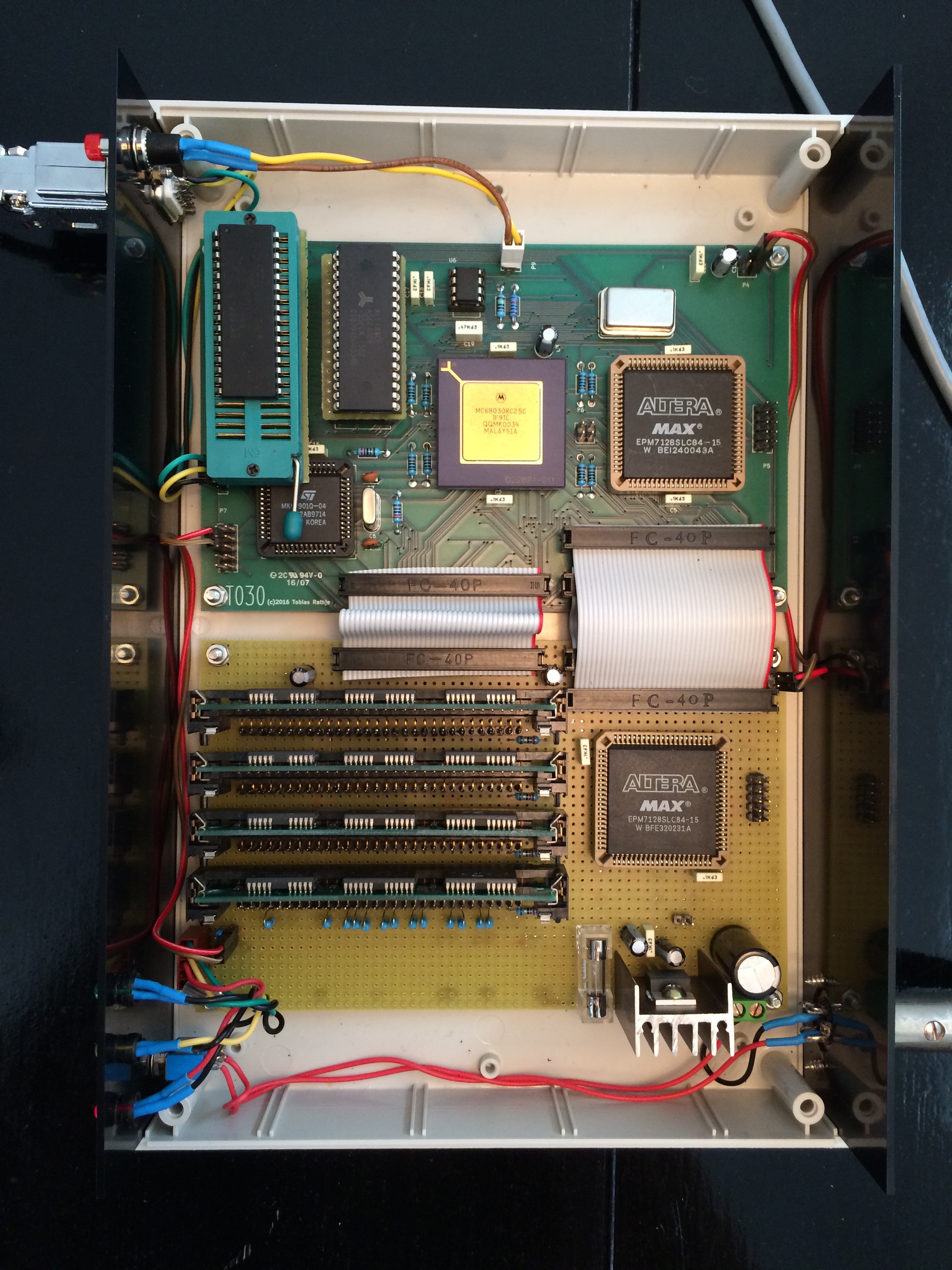
The time has come to add a lot more RAM. In order to boot a recent Linux kernel, I guess I need at least 8 MB and probably even 16 MB to be on the safe side.
32 AS6C4008's (or equivalent through hole SRAM) would require several additional boards and more importantly break the budget for this project.
So I have no other options than to dive into the wonders of dynamic RAM. After having tinkered with a DRAM extension board for a couple of weeks, I can certainly understand why a lot of hobbyists place these devices somewhere between "black magic" and "just not that easy to work with".
But now I have a 16 MB RAM board based on 4 x 4 MB 30 pin SIMM's which is stable most of the time...
 I have implemented a DRAM controller in a second MAX 7128 CPLD. The controller is implemented as a FSM in VHDL and performs CAS before RAS refresh, address mux and data size decoding. I have never used VHDL before but a design example along with some sample code from an RD document from Lattice got me going in the right direction.
The DRAM controller code could use a cleanup and several wait states could probably be eliminated, but for now I consider it a huge success that it can pass a RAM test without crashing :-)
I have also added some more bypass capacitors to even out the current spikes that the DRAMs generate.
 Tobias Rathje
Discussions
Become a Hackaday.io Member
Create an account to leave a comment. Already have an account? Log In.
Hi,
I've been looking at your code for my own project, the A030.
I've been looking to use DRAM for a very long time and finally give a go at it.
I found your VHDL code indeed as an update on the Lattice project.
i found 2 128Mb simms which are 3.3V but 5V tolerant. They appear to be working.
The RAS/CAS gets muxed using the FPGA and the 4 RAS and 4 CAS signals are generated using the same FPGA, as well the WE signal and the enable for the 74245 buffers on the Data line.
If you are interested, I'll send you the modified VHDL code.
This evening I went from 300ns to 200ns. As the DRAM can handle a 60ns read/write cycle there might be some more optimizing left.
The chips used in my SIMMS are 16Mx4 EDO DRAM, so burst cycles are also on the list. The chips used are MT4LC16M4H9. The SIMMS are 72 pins.
I've also modified the DRAM to have a proper 100us + 8x CBR cycles as the initialization.
Also trying some tricks where some of the signals are dependent on the falling_edge while others depend on the rising_edge of the clk.
Please contact me if you are interested.
As my logic analyzer I'm using a Tektronix TLA7016
Are you sure? yes | no