 Vladimir Savchenko
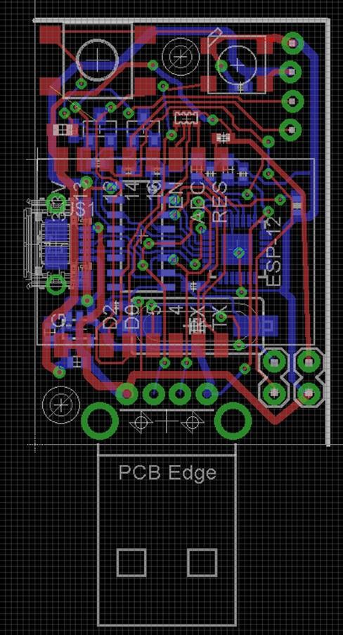
I was quite busy in the last weeks - preparing the first batch of devices for the event. While doing this it turned out that i had done some mistakes in the initial PCB design of the prototype, which made the soldering very error prone (also the fact that soldering by hand was required). This is why i designed a second revision of the PCB.
The new design is much closer to what is on the picture of the project. The main difference is that there is only 1 button and the size is 40mm length x 25 mm width.
On the other hand i did few changes to make it a bit more portable:
- Added a Micro USB port on the side
- Added 2 mounting holes
- Added one port with 2 GPIO, GND and 3.3 V
- Added second port with 2 GPIO, GND and 5 V
- Added a pad to the WS 2812B led, so that if desired - more LEDs can be attached
The goal of those modifications is to allow the board to be a bit more reusable and embeddable into devices that do slightly more. E.g. I2C, Serial communication, LED Gauge indication, etc.
I am not entirely sure that there isn't again some small mistake in this design as it will cost ~$ 150 to fix it :) But in any case i ordered 200 boards.
Discussions
Become a Hackaday.io Member
Create an account to leave a comment. Already have an account? Log In.