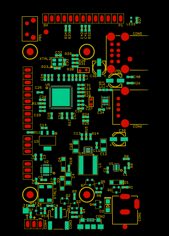
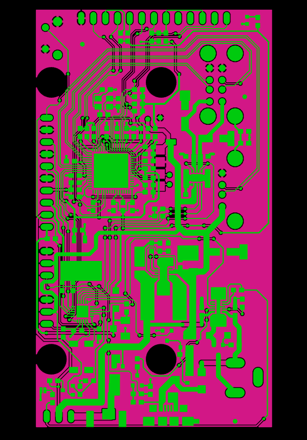
The second revision of the Pi Platter PCB is almost done. Hopefully the only additions will be various test points, if necessary, for the manufacturing test fixture. The main changes were the addition of the USB UPS bypass functionality and changing to use a stacked USB connector so the area around the PI Zero's HDMI connector was free of interference. I also slightly improved heat sinking for various parts and tightened up the high-speed signal layout as well as making sure the ground plane was improved in a few areas.
I am currently thinking the manufacturing test will be essentially a functional one, connecting to all IO ports (and any necessary other test points) and then under control of a computer we'll test the power subsystems and enumerate the USB bus and make sure we can communicate with all downstream devices. I don't think we will end up building huge volumes of this board so perhaps it's ok if the test is a little labor intensive (e.g. manually plugging in USB cables, etc.).


 Dan Julio
Discussions
Become a Hackaday.io Member
Create an account to leave a comment. Already have an account? Log In.