Russell Kramer
-
VGA Signal Generator Version2 (Diode Logic)
03/02/2016 at 05:26 • 0 commentsThe first VGA board didn't turn out the way I wanted. It was double sided and too big. I briefly considered taking the easy way out with a microcontroller, but then I realized I could make the board single sided and half the size by going even further back in time.
![]()
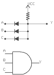
If I construct AND gates using only diodes and resistors I can avoid a spaghetti of traces running between gate ICs. I have the freedom to drop the individual diodes and resistors wherever they're most convenient.
![]()
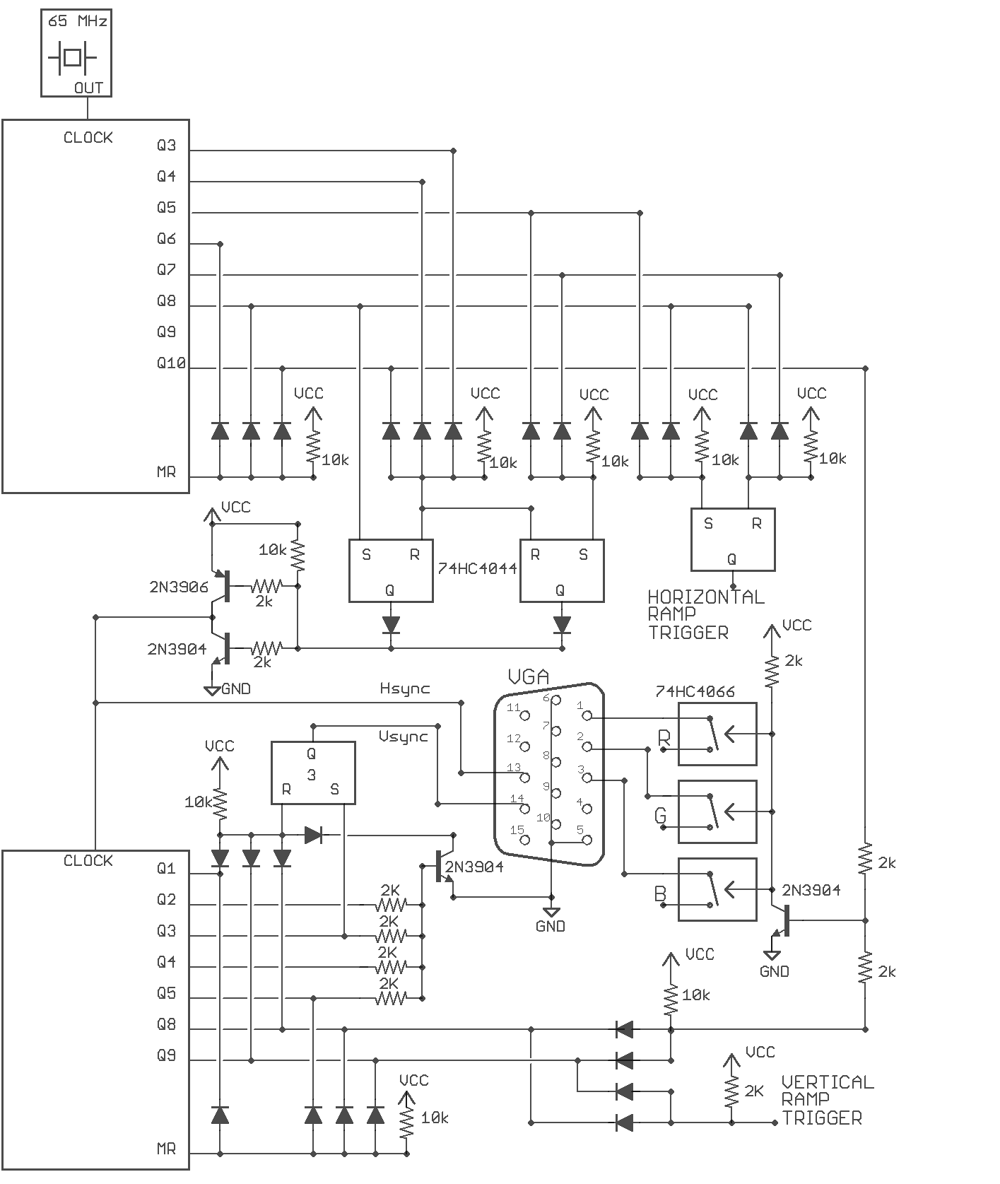
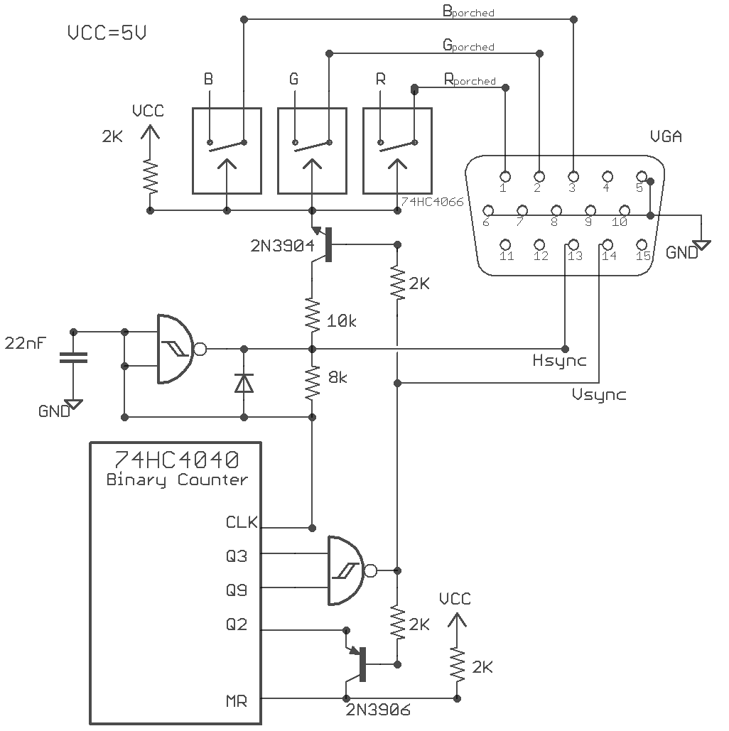
This is the VGA board redesigned using diodes for all the AND gates as well as two NOR gates implemented with resistor-transistor logic.
One of the problems with diode logic is a 0.7v drop through each gate. I needed to add an NPN PNP pair to amplify the Hsync pulse generated by the diode logic. This wasn't an issue with the Vsync pulse because it comes directly out of an SR latch.
This circuit does not generate ramps with resistor ladder DACs off the binary counters the way the last one did. Those did not cooperate with the diode logic so I went back to regulated capacitor charging (not part of this board).
This board has two outputs used to trigger the ramp pulses. There were some issues with using Hsync/Vsync pulses as ramp triggers that I'll cover later.
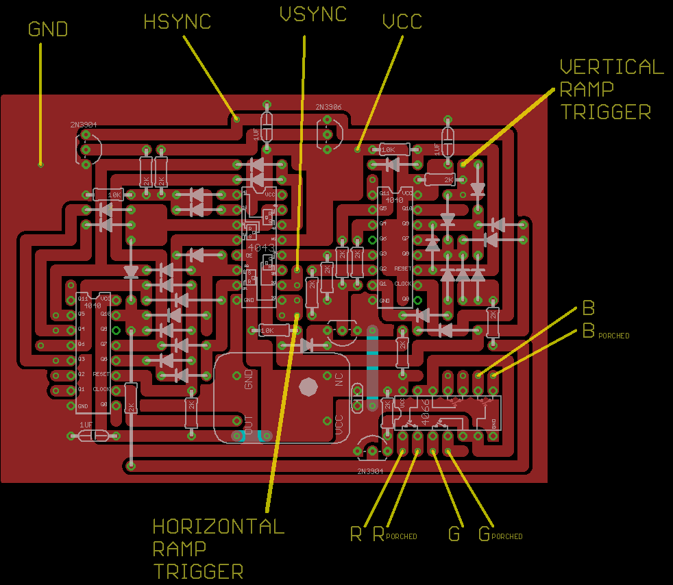
The final PCB ends up being only 3.65" x 2.55" on a single layered board and using only two jumper wires. This is half the size of the last one, and that needed to be double sided.
![]()
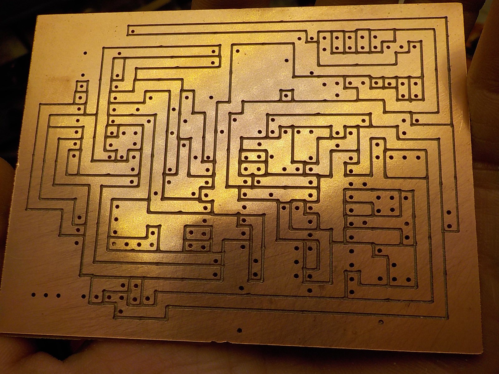
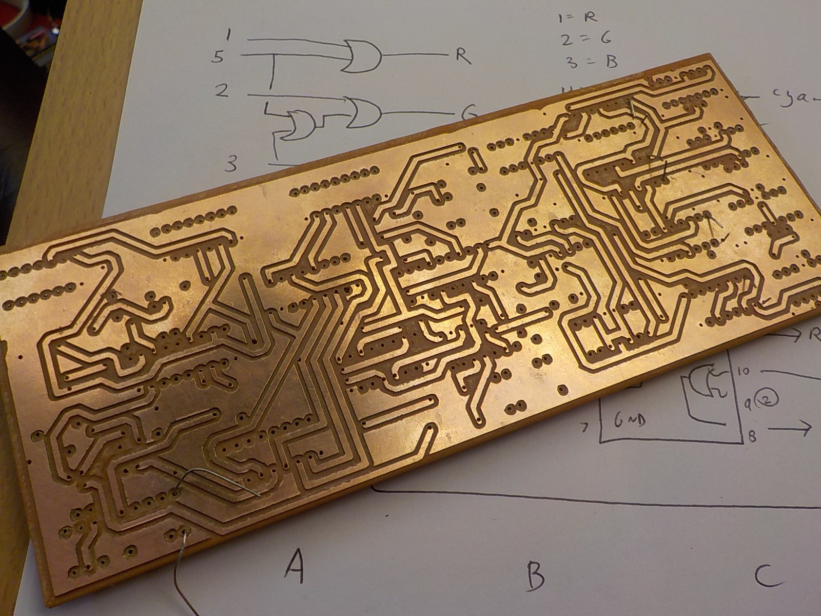
All boards in this project are designed such that they can be assembled on perfboard, but I'm taking it easy and CNCing them for now. I wrote my own G-code exporter/optimizer because I didn't like the curved trace ends and other garbage the default Eagle script produced.![]()
The soldering is a little messy because I did some debugging by cutting leads from the topside then reconnecting them. The oscillator is 66.66MHz because the 65MHz ones hadn't arrived yet.![]()
-
VGA Signal Generator Version1(aborted)
03/02/2016 at 04:06 • 0 commentsI went back to the drawing board and designed a new 1024*768-60Hz VGA signal generator based on a crystal oscillator.
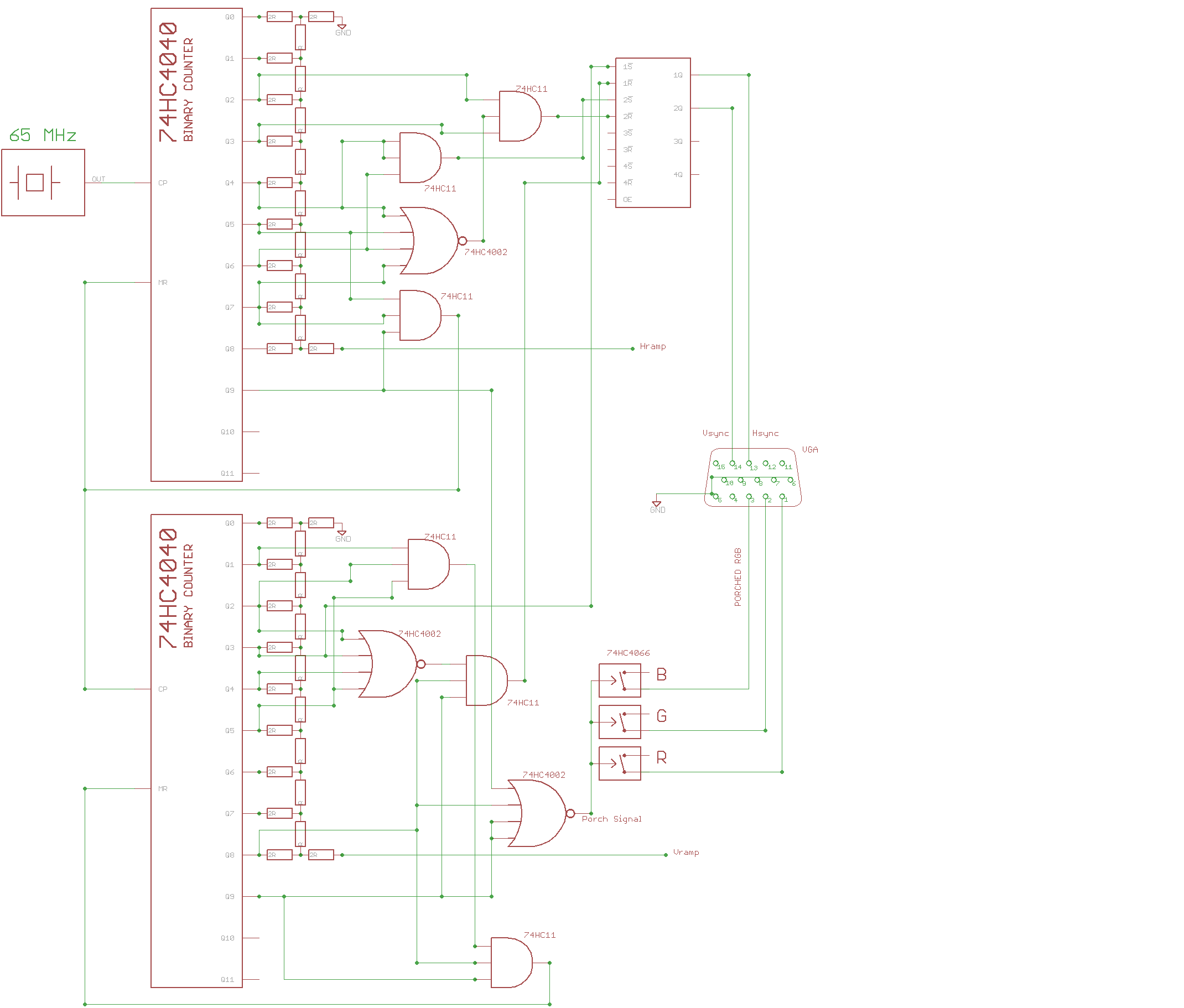
Here's the first design I came up with
![]()
In this design the ramp signals are generated with an R2R ladder DAC instead of triggering a capacitor to charge from a regulated current source.
There are two 74HC4040 Binary counters, one for horizontal timing and one for vertical timing. The horizontal 74HC4040 is clocked by a 65MHz crystal oscillator.
- After 1,024 crystal oscillations horizontal porching begins.
- After 1,048 crystal oscillations the Hsync pulse begins
- After 1,184 crystal oscillations the Hsync pulse ends.
- After 1,344 crystal oscillations the horizontal porching ends and the loop resets. (drawing the next scanline)
The vertical 74HC4040 is clocked by the end of a scanline.
- After 768 scanlines the vertical porching begins
- After 771 scanlines the Vsync pulse begins
- After 777 scanlines the Vsync pulse ends
- After 806 scanlines the loop resets (drawing the next frame)
I implemented the timing logic by running the binary counter outputs through two 74HC4002 (dual 4-input NOR gates), two 74HC11 (triple 3-input AND gates), and one 74HC4044 (Quad SR latch). The SR-latch makes logic like "keep the Vsync pulse active from 771 to 777 scanlines" a lot simpler. A karnaugh map of that logic results in half a dozen AND and OR gates. With an SR latch I only need some logic to create a pulse to turn on the latch at 771 and another pulse to turn off the latch at 777.
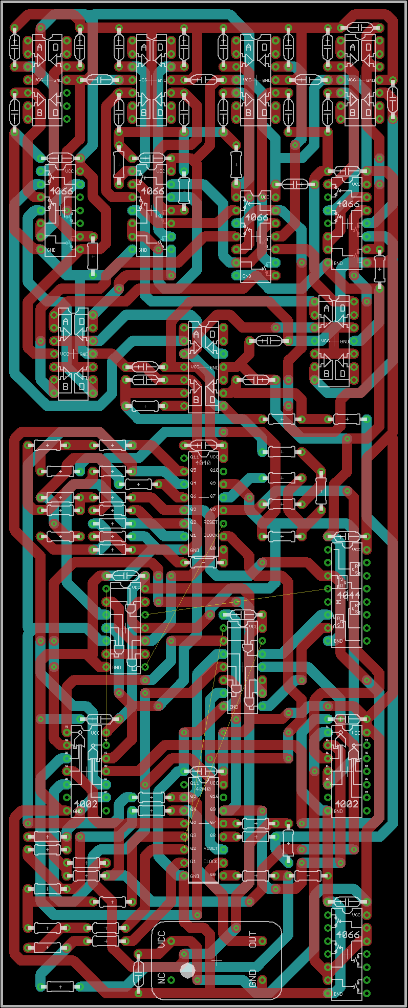
This is the PCB for the circuit. Only the bottom two-thirds are part of the VGA signal generation. The upper section is sample-and-hold circuitry that I'll cover later.
![]()
![]()
I really didn't like this board. My goal was to design all circuit boards such that they could be constructed on regular perfboard (100mil grid). This meant I needed a lot of space for the spaghetti of traces required to connect all the logic gate chips . I had to make it a double sided board with diagonal traces just to get everything hooked up (not easy to replicate on a perfboard). Even with the double layers there were still several jumper wires required.
-
Problems with the old VGA signal generator
02/24/2016 at 03:20 • 0 commentsYou should read the NES Zapper Video Synth Theremin project log before this one because this project is a direct continuation of that and there are several concepts I'm not going to cover twice.
![]()
This is the VGA signal generator used in the last project. My design goal was to keep complexity and part count down. It didn't have to be perfect ,it just had to work. There were three main problems:
- The timing was based on an resistor-capacitor oscillator, and those are notoriously unstable.
- The resolution was 640x480 which I discovered isn't supported by some newer monitors
- The RGB signal is only porched during the Sync pulses which is way outside the VGA spec.
Here's a couple examples of bugs in the old VGA circuit:
![]()
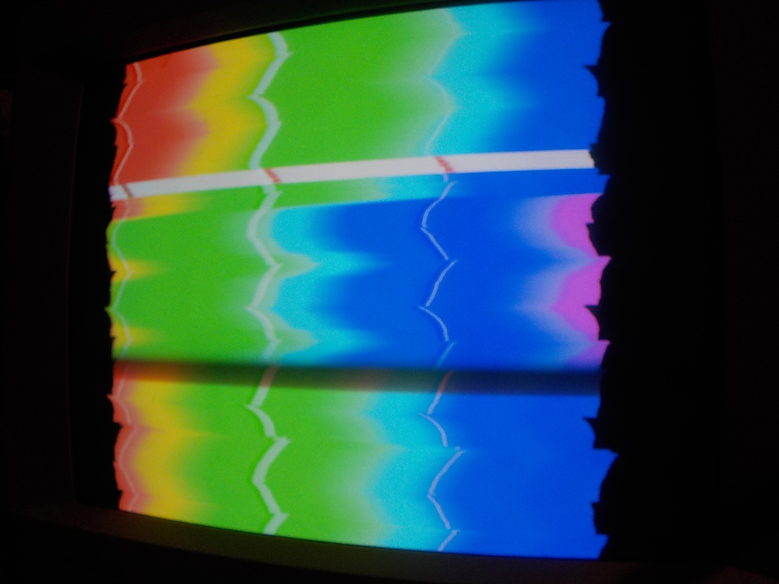
The edge of the display is jagged because of instability in the RC oscillator.
![]()
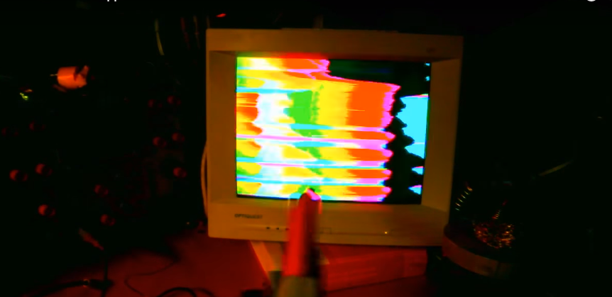
Here the oscillator gets so unstable the image tears right off the screen.
These glitches are beautiful, but I have ambitions of taking the current project to performing arts venues and connecting to their projector systems. If a projector is picky about VGA signal quality it will turn the glitches into an ugly "bad signal" blue screen. This is why I've designed a new VGA signal generator following the opposite design philosophy. This time the IBM 8514 VGA standard is being followed religiously; no more "whatever works is good enough".
Rasterphonic Glove
Analog video synthesizer you can touch with a five finger light gun. Makes music too.