Lutetium
-
Hack Chat Transcript, Part 3
09/25/2019 at 20:58 • 0 comments![]()
![]() I will be talking about PCB fab in the next viddeo. I will try and work in some of these questions into that
I will be talking about PCB fab in the next viddeo. I will try and work in some of these questions into that![]() Thanks everyone!
Thanks everyone!![]() @frank Give me an hour with ya and I could have ya doing Gig stuff!
@frank Give me an hour with ya and I could have ya doing Gig stuff!![]() I'm just a programmer, tinkering a bit with hardware :-)
I'm just a programmer, tinkering a bit with hardware :-)![]() Didn't wanna interrupt earlier with an off-topic question... but hopefully ok now to ask if anyone's done a PCB design using 0.4 mm pitch BGA? I'm considering one soon (a 36 pin BGA). Any tips?
Didn't wanna interrupt earlier with an off-topic question... but hopefully ok now to ask if anyone's done a PCB design using 0.4 mm pitch BGA? I'm considering one soon (a 36 pin BGA). Any tips?![]() Just to add, the stuff we did on 2 sided boards in the 80's was just awful, I would use 40-80 series resistors in a design
Just to add, the stuff we did on 2 sided boards in the 80's was just awful, I would use 40-80 series resistors in a design![]() @Paul Stoffregen Are you doing it yourself? What CAD package?
@Paul Stoffregen Are you doing it yourself? What CAD package?![]() Yup. I'm a bit embarrassed to admit it, but I use an ancient version of PADS. It still works pretty well for me.
Yup. I'm a bit embarrassed to admit it, but I use an ancient version of PADS. It still works pretty well for me.![]() @Frank Buss you know this stuff. You were asking the right questions in that other forum on FB. ;)
@Frank Buss you know this stuff. You were asking the right questions in that other forum on FB. ;)![]() @Paul Stoffregen 0.4mm pitch - you will have to use Via-In-Pad HDI
@Paul Stoffregen 0.4mm pitch - you will have to use Via-In-Pad HDI![]() PADs is one of the progenitors of the industry.
PADs is one of the progenitors of the industry.![]() I have a reference design I can send you with a freescale I.MX8 CPU if you like?
I have a reference design I can send you with a freescale I.MX8 CPU if you like?![]() I guess that means I need to learn how to buy a PCB with via-in-pad... never done that befer
I guess that means I need to learn how to buy a PCB with via-in-pad... never done that befer![]() *before
*before![]() @Ben Jordan I would love a copy if you could email me at bilherd@hackaday dot com
@Ben Jordan I would love a copy if you could email me at bilherd@hackaday dot com![]() will do
will do![]() @Paul Stoffregen you might be able to use thin traces which is slightly cheaper.
@Paul Stoffregen you might be able to use thin traces which is slightly cheaper.![]() I've never had a manufacturer complain about via-in-pad, and I don't take any special steps to warn them or anything
I've never had a manufacturer complain about via-in-pad, and I don't take any special steps to warn them or anything![]()
Hack Chat Transcript, Part 1 | Details | Hackaday.io
Well, we've been having some good sidebar discussion here for a bit, but let's kick it off officially and welcome Bil Herd to the Hack Chat. Today we're going to learn about high-speed PCB design. Bil, I usually ask hosts to introduce themselves to get things going, but that seems silly here.
![]() so you give them more than one drill file?
so you give them more than one drill file?![]() generally they know how to do it these days...
generally they know how to do it these days...![]() I know someone that is as dedicated to PCB layout as I am to hardware. I run questions like .4mm by him in the form of "yes buyt what works in production?"
I know someone that is as dedicated to PCB layout as I am to hardware. I run questions like .4mm by him in the form of "yes buyt what works in production?"![]() no, are you referring to via-in-pad with filling or something?
no, are you referring to via-in-pad with filling or something?![]() yes different drill files for each drill layer pair will be needed
yes different drill files for each drill layer pair will be needed![]() We were talking earlier about via in pad and sealing them and hot gasses
We were talking earlier about via in pad and sealing them and hot gasses![]() yeah if it's hdi, fabs will often plate them up to solid copper - no outgassing problems there
yeah if it's hdi, fabs will often plate them up to solid copper - no outgassing problems there![]() ballpark figures may be obtained by US based fabs
ballpark figures may be obtained by US based fabs![]() I just read "The Designer's HANDBOOK for DFM" by Sierra Circuits, (DFM is design for manufacturing), I recommend it
I just read "The Designer's HANDBOOK for DFM" by Sierra Circuits, (DFM is design for manufacturing), I recommend it![]() was going to mentione Sierra!
was going to mentione Sierra!![]() @Bil Herd do you mean this?
@Bil Herd do you mean this?https://www.facebook.com/groups/CommanderX16/permalink/524160045001761/?comment_id=524251758325923&reply_comment_id=524333631651069
I think they will get into trouble, when they try to access the YM2151 with an 8 MHz clocked X16, it just works by chance now. But at least they can switch it to 4 MHz, but I think a latch to make the signal and data longer would be better.
![]() I am looking for the link, a good read for 80 pages... of course I printed it rather than read it online
I am looking for the link, a good read for 80 pages... of course I printed it rather than read it online![]() @Frank Buss ;)
@Frank Buss ;)![]() What website do you recommend to ask specific question about high speed/RF magic in PCB designs?
What website do you recommend to ask specific question about high speed/RF magic in PCB designs?![]() Check out the Signal Integrity Journal , give me a sec and I will pull links.
Check out the Signal Integrity Journal , give me a sec and I will pull links.![]() looks like there are other things they do by trial and error, like using a TL084 with just +5V / 0V. The designer said it works stable with a big enough capacitor :-)
looks like there are other things they do by trial and error, like using a TL084 with just +5V / 0V. The designer said it works stable with a big enough capacitor :-)![]()
DFM_handbook_digital.pdf
1 MB
![]() See if that pdf is readable.\
See if that pdf is readable.\![]() yup, got it, 77 pages :)
yup, got it, 77 pages :)![]() @Frank Buss ;)
@Frank Buss ;)![]() because you said i was talking about differential pairs, i actually wasn't it just got recommended to me to keep all datalines at the same length because the protocoll is counting on them to arrive at the same time, so does that not actually matter?
because you said i was talking about differential pairs, i actually wasn't it just got recommended to me to keep all datalines at the same length because the protocoll is counting on them to arrive at the same time, so does that not actually matter?![]()
Teledyne LeCroy SI Academy
Learn signal integrity problem solving skills from the Signal Integrity Evangelist, Dr. Eric Bogatin. Did you miss one of Eric's popular live classes? At the Teledyne LeCroy Signal Integrity Academy, you can explore all his past classes and many new ones, broken down into short, concise, video lessons.
![]() I remember an older engineer telling me about how he used hex inverter chips as opamps, quite interesting
I remember an older engineer telling me about how he used hex inverter chips as opamps, quite interesting![]() @aerispalm not NEAR as critical as we used to say, in fact I have changed my viewpoint a little.
@aerispalm not NEAR as critical as we used to say, in fact I have changed my viewpoint a little.![]() If you are off by half an inch at 2/3rds the speed of ligh you are still pretty darn close
If you are off by half an inch at 2/3rds the speed of ligh you are still pretty darn close![]() light
light![]() a signal propagates 6" in a ns on a standard PCB
a signal propagates 6" in a ns on a standard PCB![]() its like square corners, which we didn't get to, it goes by so dang fast that it gets lost in a rounding error
its like square corners, which we didn't get to, it goes by so dang fast that it gets lost in a rounding error![]() @Adam Oakley how does this work? an inverter gate has only one input
@Adam Oakley how does this work? an inverter gate has only one input![]()
https://speedingedge.com/products/right-first-time/
Right the First Time, A Practical Handbook on High-Speed PCB and System Design
"Right the First Time, A Practical Handbook on High Speed PCB and System Design, Volume 1," is the premier publication of Speeding Edge. It was written by Speeding Edge founder and president, Lee W. Ritchey, co-authored by John Zasio, an recognized industry expert in high-speed design, and edited by Kella J.
![]() Whoops that was meant to be a link to Lee's site, not an ad for his book
Whoops that was meant to be a link to Lee's site, not an ad for his book![]() I wish I had asked more about that, something about biasing it in a certain way to use it as an amplifier
I wish I had asked more about that, something about biasing it in a certain way to use it as an amplifier![]()
https://www.signalintegrityjournal.com/
Home Page
Signal Integrity Journal, a sister publication to Microwave Journal, covers signal integrity, power integrity and EMC/EMI related topics with industry news, technical articles, white papers, products, Buyer's Guide, webinars, videos and more. The vision for the SI Journal is to increase the signal to noise ratio for SI, PI and EMC engineers by providing high value content.
Read this on Signalintegrityjournal
![]() We have changed what we thought we knew about decoupling caps, now we get caught in the anti-resonance of teh caop since caps are also.... wait for it... Inductors
We have changed what we thought we knew about decoupling caps, now we get caught in the anti-resonance of teh caop since caps are also.... wait for it... Inductors![]() "the decoupling cap"
"the decoupling cap"![]() https://wiki.analog.com/university/courses/electronics/electronics-lab-20 here's an article about the hex inverter amplifier
https://wiki.analog.com/university/courses/electronics/electronics-lab-20 here's an article about the hex inverter amplifier![]() Interesting. I'll look into it.
Interesting. I'll look into it.![]() thanks, looks like an interesting hack :-)
thanks, looks like an interesting hack :-)![]() I used to bias the 4000 series CMOS inverters into amps. I made an ultrasonic blind spot detector in the 80's that fit in a running light using ahex invertors as analog amps
I used to bias the 4000 series CMOS inverters into amps. I made an ultrasonic blind spot detector in the 80's that fit in a running light using ahex invertors as analog amps -
Hack Chat Transcript, Part 2
09/25/2019 at 20:07 • 0 comments![]() Well crap that didnt work
Well crap that didnt work![]()
![]()
![]() I blame Google
I blame Google![]()
![]()
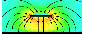
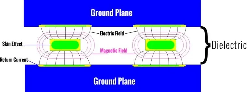
![]() So these images show a trace above a ground plane and the field around it.
So these images show a trace above a ground plane and the field around it.![]() Got it, thanks
Got it, thanks![]() strawberry fields forever?
strawberry fields forever?![]() So when we DONT match the impedance a reflection occurs. Truth be told we live with tehse reflections all over the place but...
So when we DONT match the impedance a reflection occurs. Truth be told we live with tehse reflections all over the place but...![]() Enter the series resistor, I used to put 22 Ohm resistors in series to absorb the signal that got away from me and is bouncing up and down the trace
Enter the series resistor, I used to put 22 Ohm resistors in series to absorb the signal that got away from me and is bouncing up and down the trace![]() are termination resistors fitting into this picture too or no?
are termination resistors fitting into this picture too or no?![]() A reflection occurs when the receiver doesn't absorb 100% of the signal
A reflection occurs when the receiver doesn't absorb 100% of the signal![]() if the transmitter is 50Ohms and the receiver is 55 ohms than a percentage will be reflected.
if the transmitter is 50Ohms and the receiver is 55 ohms than a percentage will be reflected.![]() If the transmitter doesn't absorb it it will be reflected again
If the transmitter doesn't absorb it it will be reflected again![]() Is that kinda clear or should I talk more about absobing the reflection when they ARENT matched?
Is that kinda clear or should I talk more about absobing the reflection when they ARENT matched?![]() By the way, my CAD package calculates the trace width for me
By the way, my CAD package calculates the trace width for me![]() which?
which?![]() (CAD package)
(CAD package)![]() Altium, Labcenter
Altium, Labcenter![]() Eagle might, Ted you still there?
Eagle might, Ted you still there?![]() Labcenter makes Proteus. Kicad also will with the right addon
Labcenter makes Proteus. Kicad also will with the right addon![]() So from my understanding by adding a serial R on the tx side we allow the signal to reflect from unmatched receiver and to be absorbed at the receiver side. And that does not influence the reception quality because the receiver does not "see" the reflection caused by itself?
So from my understanding by adding a serial R on the tx side we allow the signal to reflect from unmatched receiver and to be absorbed at the receiver side. And that does not influence the reception quality because the receiver does not "see" the reflection caused by itself?![]() Yes. AND its not radiated as much and it doesn't keep bouncing around creating noise, including FCC emmision noise
Yes. AND its not radiated as much and it doesn't keep bouncing around creating noise, including FCC emmision noise![]() right
right![]() I think using firehose to fill a small cup vs. using garden hose vs. using garden hose with restrictor attachment
I think using firehose to fill a small cup vs. using garden hose vs. using garden hose with restrictor attachment![]() is that right direction? "spilled water" in my analogy would be reflected signal
is that right direction? "spilled water" in my analogy would be reflected signal![]() I am trying to get images off my CAD station but the image upload problem is making it tough
I am trying to get images off my CAD station but the image upload problem is making it tough![]() Think of a trough of water.
Think of a trough of water.![]() But the restrictor is on the tap and the cup is a closed system
But the restrictor is on the tap and the cup is a closed system![]() and a wave
and a wave![]()
![]()
![]() Cheap PCB material has a more variable Dielectric constant and more absorption in general usually. Oshpark has a good hi freq material (FR408) for their 4 layer boards and JLBPCB has some Rogers materials available (I use 2313)
Cheap PCB material has a more variable Dielectric constant and more absorption in general usually. Oshpark has a good hi freq material (FR408) for their 4 layer boards and JLBPCB has some Rogers materials available (I use 2313)Flex pcb material polyamide also has good hifreq properties.
![]() Also before I forget there are great calculators for some of this online. So if I move into wave length these here may help: https://www.microwaves101.com
Also before I forget there are great calculators for some of this online. So if I move into wave length these here may help: https://www.microwaves101.comhttps://www.everythingrf.com/rf-calculators
![]() As frequencies go up, the distance represented by a wavelength goes down.
As frequencies go up, the distance represented by a wavelength goes down.![]() Everyone understand what I mean by wavelenth? Basically Planks constant and why those little holes in yoru microwave oven door let light out but keep microwaves in
Everyone understand what I mean by wavelenth? Basically Planks constant and why those little holes in yoru microwave oven door let light out but keep microwaves in![]() 250 mhz has a wavelength of 47”, 500 mhz has a wavelength of 23”
250 mhz has a wavelength of 47”, 500 mhz has a wavelength of 23”![]() Sounds huge right!
Sounds huge right!![]() When a trace gets to be 1/4th of a wavelength we really DO need to start using atransmission line
When a trace gets to be 1/4th of a wavelength we really DO need to start using atransmission line![]() (transmission line = stripline = trave over ground plane)
(transmission line = stripline = trave over ground plane)![]() So if we have 500mhz component, anything near 6”/150mm or greater needs to be done as transmission line known as a microstrip and others like stripline, waveguide, etc
So if we have 500mhz component, anything near 6”/150mm or greater needs to be done as transmission line known as a microstrip and others like stripline, waveguide, etc![]() so think 500Mhz and 6" , at 500 mhz RADIAN Freq or rise time
so think 500Mhz and 6" , at 500 mhz RADIAN Freq or rise time![]() the trace officially becomes an RF antenna at 6"
the trace officially becomes an RF antenna at 6"![]() so with a 100mhz PCIe it's pretty much everything needs to be a transmission line?
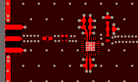
so with a 100mhz PCIe it's pretty much everything needs to be a transmission line?![]() Here is a radar I am working and will be in a future video
Here is a radar I am working and will be in a future video![]() Awesome free calculators: AppCAD (available free by Avago web site). QUCS (open source simulator, has awesome and very accurate T-line solver in it) qucs.sourceforge.net
Awesome free calculators: AppCAD (available free by Avago web site). QUCS (open source simulator, has awesome and very accurate T-line solver in it) qucs.sourceforge.net![]() Whats the risetime of the signal though?
Whats the risetime of the signal though?![]() mmm
mmm![]() PCIE Gen 4 is a tough nut, all is doen as controlled impedance
PCIE Gen 4 is a tough nut, all is doen as controlled impedance![]() QUOCs rocks.
QUOCs rocks.![]() Hi Ben!
Hi Ben!![]() Hey Bil!!
Hey Bil!!![]()
![]()
![]() NICE
NICE![]() looks like you made a PCB coax almost?
looks like you made a PCB coax almost?![]() So here is a trace coming in on the left, there is an SMA connector soldered there and the cone tries to smoothly transition the signal from the connector to the PCB
So here is a trace coming in on the left, there is an SMA connector soldered there and the cone tries to smoothly transition the signal from the connector to the PCB![]() YES! We are making coaxes out of PCBs
YES! We are making coaxes out of PCBs![]() what kind of frequency is this designed for?
what kind of frequency is this designed for?![]() So the vias right along the trace are "shielding" vias but also stitch the return path in the inner layer to the shield on the top layer
So the vias right along the trace are "shielding" vias but also stitch the return path in the inner layer to the shield on the top layer![]() 2.54ghz and higher
2.54ghz and higher![]() It starts getting iffy when half wavelength equals the via period.
It starts getting iffy when half wavelength equals the via period.![]() We use the smallest parts we can typically, there are tricks like flipping teh inductor over and soldering them upside down to make the path and inductance shorter
We use the smallest parts we can typically, there are tricks like flipping teh inductor over and soldering them upside down to make the path and inductance shorter![]() Yup. So notice all of the other vias, (this is about an x2 or x3 view bytw)
Yup. So notice all of the other vias, (this is about an x2 or x3 view bytw)![]() btw
btw![]() at 1/20th of a wavelenth the shield can start to "stand", little resonances build up
at 1/20th of a wavelenth the shield can start to "stand", little resonances build up![]() Think of a sheet blowing in the wind. and then start tacking it down every few inches, same concept
Think of a sheet blowing in the wind. and then start tacking it down every few inches, same concept![]() I am out of time and don't think I explained this very well, (don't ever tear a finger off, it screws with your typing)
I am out of time and don't think I explained this very well, (don't ever tear a finger off, it screws with your typing)![]() Good timing, Bil...
Good timing, Bil...So I hate to break up the party, but we're coming to the one-hour mark and we need to let Bil get back to work if he needs to. Feel free to stick around and keep the chat going, though, if time allows. For now, I'll just say thanks to Bil for stepping up on short notice, and for the great chat - I learned a lot.
![]() thanks for explaining what you did. Much appreciated.
thanks for explaining what you did. Much appreciated.![]() Did anybody get something they didn't previously know?
Did anybody get something they didn't previously know?![]() Thanks Bill
Thanks Bill![]() Absolutely!
Absolutely!![]() Yeah, this was great!
Yeah, this was great!![]() I recommend the video I referenced above as I talk faster than I type
I recommend the video I referenced above as I talk faster than I type![]() which video?
which video?![]() Thanks for this, i get it a lot more, but still have a way to go
Thanks for this, i get it a lot more, but still have a way to go![]() @Dan Maloney The image paste thing seems to be a mode it gets into with a keystroke, I just don't know which keys
@Dan Maloney The image paste thing seems to be a mode it gets into with a keystroke, I just don't know which keys![]() Yes, thanks. Your video/blogs have been very informative, too. Look forward to more.
Yes, thanks. Your video/blogs have been very informative, too. Look forward to more.![]() I'll be posting a transcript with links in a few minutes
I'll be posting a transcript with links in a few minutes![]() The pics were great
The pics were great![]() Yeah, thanks!
Yeah, thanks!![]() Yeah, I'm going to experiment with that for future chats. Sorry for the trouble
Yeah, I'm going to experiment with that for future chats. Sorry for the trouble![]()
https://www.youtube.com/watch?v=STCGzanAyR0
![]() Thanks to everyone for coming. Don't forget that next week we'll be talking about Alternative Photography with Pierre-Loup Martin
Thanks to everyone for coming. Don't forget that next week we'll be talking about Alternative Photography with Pierre-Loup Martin![]()
https://hackaday.io/event/166697-alternative-photography-hack-chat
Alternative Photography Hack Chat
Pierre-Loup Martin joins us for the Hack Chat on Wednesday, October 2, 2019 at noon PDT. Time zones got you down? Here's a handy time converter! It seems like the physics of silicon long ago replaced the chemistry of silver as the primary means of creating photographs, to the point where few of us even have film cameras anymore, and home darkrooms are a relic of the deep past.
![]() you rock Bil!
you rock Bil!![]() Ask Ben if he wrote that part of the app. ;)
Ask Ben if he wrote that part of the app. ;)![]()
https://hackaday.com/2018/09/28/inductance-in-pcb-layout-the-good-the-bad-and-the-fugly/
Inductance In PCB Layout: The Good, The Bad, And The Fugly
When current flows through a conductor it becomes an inductor, when there is an inductor there is an electromagnetic field (EM). This can cause a variety of issues during PCB layout if you don't plan properly, and sometimes we get burned even when we think we have planned for unwanted inductance and the effects that come with them.
thanks @Bil Herd , I didn't understand before your chat why the trace width is important for the impedance, but makes sense now, being a capacitor
-
Hack Chat Transcript, Part 1
09/25/2019 at 20:06 • 0 commentsWell, we've been having some good sidebar discussion here for a bit, but let's kick it off officially and welcome Bil Herd to the Hack Chat. Today we're going to learn about high-speed PCB design.
Bil, I usually ask hosts to introduce themselves to get things going, but that seems silly here. Maybe just a quick intro?
![]() Hi all, I do the odd video for HAD and recently did a couple about high speed PCB stuff and have another video comoing about PCBs themselves
Hi all, I do the odd video for HAD and recently did a couple about high speed PCB stuff and have another video comoing about PCBs themselves![]() OK, thanks. I am just trying them out to save space as a low power FET, but they are already causing more problems than their worth.
OK, thanks. I am just trying them out to save space as a low power FET, but they are already causing more problems than their worth.![]() My background was that I had a backyard full of TV chassis in the '70s, never finished high school and ended up designing computers for Commodore Business Machines
My background was that I had a backyard full of TV chassis in the '70s, never finished high school and ended up designing computers for Commodore Business Machines![]() i actually got away with just making sure all connections are the same length and having a groundplane for 100 mhz qspi, i think anyways i guess its possible that the mcu is throttling .
i actually got away with just making sure all connections are the same length and having a groundplane for 100 mhz qspi, i think anyways i guess its possible that the mcu is throttling .![]() experience is the best teacher. nice.
experience is the best teacher. nice.![]() So first let me throw a link to the high speehttps://hackaday.com/2019/01/24/video-putting-high-speed-pcb-design-to-the-test/d Hackaday post which I will be referring to a bunch:
So first let me throw a link to the high speehttps://hackaday.com/2019/01/24/video-putting-high-speed-pcb-design-to-the-test/d Hackaday post which I will be referring to a bunch:![]() High speed pcb design to me, means understanding about impedance, which is the combination of the effects of capacitance and inductance.
High speed pcb design to me, means understanding about impedance, which is the combination of the effects of capacitance and inductance.![]()
https://hackaday.com/2019/01/24/video-putting-high-speed-pcb-design-to-the-test/
Video: Putting High Speed PCB Design To The Test
Designing circuit boards for high speed applications requires special considerations. This you already know, but what exactly do you need to do differently from common board layout? Building on where I left off discussing impedance in 2 layer Printed Circuit Board (PCB) designs, I wanted to start talking about high speed design techniques as they relate to PCBs.
![]() When we go up in speeds it means that not only do we have to get fast signals moving around the board but also that the power supply is able to deliver current very quickly while maintain voltage regulation and stability. The two of these things are often referred to these days as Signal Integrity or SI.
When we go up in speeds it means that not only do we have to get fast signals moving around the board but also that the power supply is able to deliver current very quickly while maintain voltage regulation and stability. The two of these things are often referred to these days as Signal Integrity or SI.![]() A vital part of high-speed design is understanding that the PCB is an entrenched component of the design. It has differing amounts of inductance and capacitance depending on the traces and planes and it can absorb energy or even resonant.
A vital part of high-speed design is understanding that the PCB is an entrenched component of the design. It has differing amounts of inductance and capacitance depending on the traces and planes and it can absorb energy or even resonant.![]() PCB high speed design is black magic
PCB high speed design is black magic![]() If we have time I can talk about differential signals such as @aerispalm just mentioned.
If we have time I can talk about differential signals such as @aerispalm just mentioned.![]() Hi Frank, I know you well enough to know that Hi Speed / RF design is just an extension of what you already do and know
Hi Frank, I know you well enough to know that Hi Speed / RF design is just an extension of what you already do and know![]() thanks, I'm a black magic apprentice :-)
thanks, I'm a black magic apprentice :-)![]() First thing I harp on is inductance and the understanding that inductance increases based on the distance to the return path, the width of the trace is minor compared to the distance
First thing I harp on is inductance and the understanding that inductance increases based on the distance to the return path, the width of the trace is minor compared to the distance![]() what is the "dividing line" for high speed signals? 50Mhz? 100Mhz? 10Mhz? Like when does it really start to matter?
what is the "dividing line" for high speed signals? 50Mhz? 100Mhz? 10Mhz? Like when does it really start to matter?![]() Inductance resists a change in current, so as you might expect is bad for delivering current quickly. Capacitance resists a change in voltage so good for power supply, bad for signals.
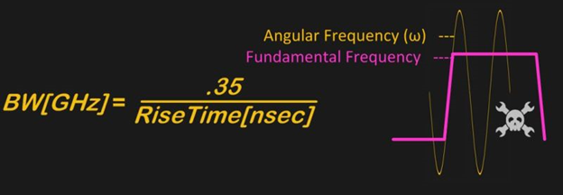
Inductance resists a change in current, so as you might expect is bad for delivering current quickly. Capacitance resists a change in voltage so good for power supply, bad for signals.![]() When we talk about frequency we usually mean the rising and falling edges, which typically has more hi-freq content then the fundamental signal itself, I.E. the rising edge of a 10mhz clock might have 100-200mghz of ‘radian/angular’ frequency
When we talk about frequency we usually mean the rising and falling edges, which typically has more hi-freq content then the fundamental signal itself, I.E. the rising edge of a 10mhz clock might have 100-200mghz of ‘radian/angular’ frequency![]() so speed of edges is as/more important than fundamental. Got it.
so speed of edges is as/more important than fundamental. Got it.![]() @Dave Blundell For me its when the radian frequency gets over 300 mhz, but its not a sharp edge, the faster my riser times the more careful I am
@Dave Blundell For me its when the radian frequency gets over 300 mhz, but its not a sharp edge, the faster my riser times the more careful I am![]() Sorry instead of sharp edge, I meant its not a certain frequency below which you can do anything and above it is considered to be hi freq
Sorry instead of sharp edge, I meant its not a certain frequency below which you can do anything and above it is considered to be hi freq![]() luckily with modern chips, you can set the slew rate of IOs, so that it doesn't get too high
luckily with modern chips, you can set the slew rate of IOs, so that it doesn't get too high![]() Here is what I mean by radian freq
Here is what I mean by radian freq![]()
![]()
![]() so adding a couple pf of capacitance to high-ish lines close coupled is a way to slow down edges and not have to worry about high speed design?
so adding a couple pf of capacitance to high-ish lines close coupled is a way to slow down edges and not have to worry about high speed design?![]() Lol... yes, don't court problems when you don't need to.
Lol... yes, don't court problems when you don't need to.![]() as muhc?
as muhc?![]() A cap coould cause most of the signal to be reflected if it creates an incongruence, I.e. a sudden change in the impedance of the trace.
A cap coould cause most of the signal to be reflected if it creates an incongruence, I.e. a sudden change in the impedance of the trace.![]() So for hi speed it is more important to have small distance between PCB layers (signal and its return plane) than paying attention to the width of the signal trace itself ?
So for hi speed it is more important to have small distance between PCB layers (signal and its return plane) than paying attention to the width of the signal trace itself ?![]() ooh @Bil Herd that angular vs fundamental freq diagram is great. I learned something already :)
ooh @Bil Herd that angular vs fundamental freq diagram is great. I learned something already :)![]() First lets talk about how signals propogate, hint at the frequencies I am talking about its NOT electrons
First lets talk about how signals propogate, hint at the frequencies I am talking about its NOT electrons![]() I think adding capacitors is not good, isn't the usual practice a source termination series resistor?
I think adding capacitors is not good, isn't the usual practice a source termination series resistor?![]() @MatYay remind me about thinkness in a sec
@MatYay remind me about thinkness in a sec![]() The high speed component is an EM wave! No mass
The high speed component is an EM wave! No mass![]() Series resistors near the driving pin have usually been my go-to solution. Curious if there are better ways?
Series resistors near the driving pin have usually been my go-to solution. Curious if there are better ways?![]() EM = electromagnetic... as in Maxwell
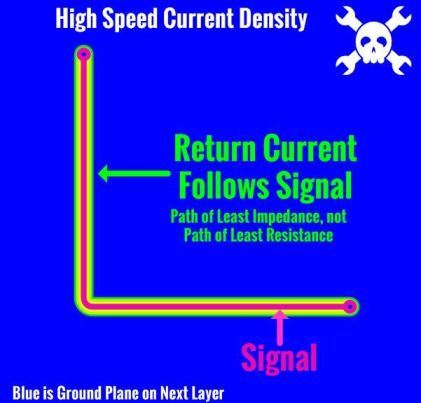
EM = electromagnetic... as in Maxwell![]() At high freq the current follows the path of least impedance, not least resistance!
At high freq the current follows the path of least impedance, not least resistance!![]()
![]()
![]() Mr. Applied Science did a good video series on impedance:
Mr. Applied Science did a good video series on impedance:![]() In the example above a DC current flow would go diagonally, but at 500mhz it will follow the trace in both directions
In the example above a DC current flow would go diagonally, but at 500mhz it will follow the trace in both directions![]() Yes. A transmission line works by creating a consistent impedance, such as 50 ohms or 100-120 ohms. Impedance is the combination of the capacitance (XC or capacitive reactance) and inductance (XL or inductive reactance) plus any regular-ole-resistance that is present.
Yes. A transmission line works by creating a consistent impedance, such as 50 ohms or 100-120 ohms. Impedance is the combination of the capacitance (XC or capacitive reactance) and inductance (XL or inductive reactance) plus any regular-ole-resistance that is present.![]() So we not only want low impedance but we want a smooth consisten ride for the signal as it goes snapping down the trace.
So we not only want low impedance but we want a smooth consisten ride for the signal as it goes snapping down the trace.![]() consistent
consistent![]() what happens if there is no ground plane below the signal trace?
what happens if there is no ground plane below the signal trace?![]() it's an inductor!
it's an inductor!![]() Thing of a wave flowing through water in a trough and suddenly the trough gets smaller, you will see the part of the wave that didn't fit into the smaller trough get reflected back since it has no-where else to goa
Thing of a wave flowing through water in a trough and suddenly the trough gets smaller, you will see the part of the wave that didn't fit into the smaller trough get reflected back since it has no-where else to goa![]() think
think![]() Hi Ted! Yes a straight out inductor. A example of a bad situation is shown here:
Hi Ted! Yes a straight out inductor. A example of a bad situation is shown here:![]()
![]()
![]() And inductors resist a change in current. Inductance can be hHUGE without a nearby return path
And inductors resist a change in current. Inductance can be hHUGE without a nearby return path![]() Here is an example of too much inductance at even low frequencies:
Here is an example of too much inductance at even low frequencies:![]() Why would that return path be the path of least impedance?
Why would that return path be the path of least impedance?![]()
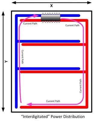
Interdigitated Power Distribution
Interdigitated power distribution results in a larger area and higher inductance.
![]() Just because there's "nothing in the way"?
Just because there's "nothing in the way"?![]() Crap, image isn't pasting, give me a sec (I hate technology)
Crap, image isn't pasting, give me a sec (I hate technology)![]()
https://hackaday.com/wp-content/uploads/2018/09/interdigitated2-e1537281708645.jpg
![]()
![]()
![]() Dan, I cant past anymore, I have to upload.
Dan, I cant past anymore, I have to upload.![]() Yeah, same thing happened to me. Odd.
Yeah, same thing happened to me. Odd.![]() are blue/red top/bottom tin that pic?
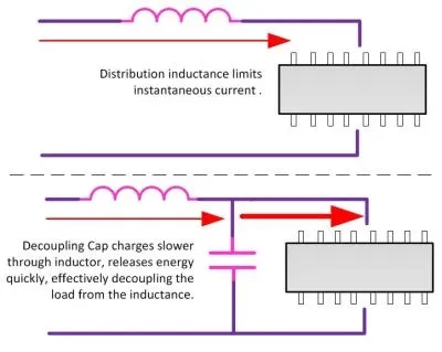
are blue/red top/bottom tin that pic?![]() So everybody is aware of decoupleing caps, but do you know WHAT is being decoupled?
So everybody is aware of decoupleing caps, but do you know WHAT is being decoupled?![]() Thanks Dan, I have to sanity check myself every day and thought I failed for the day. :)
Thanks Dan, I have to sanity check myself every day and thought I failed for the day. :)![]() decoupling: local source of current vs. needing to pump it from elsewhere
decoupling: local source of current vs. needing to pump it from elsewhere![]() So its the inductance, or "resistance to changes in current" that we have to decouple:
So its the inductance, or "resistance to changes in current" that we have to decouple:![]()
![]()
![]() Impedance is the combination of the capacitance (XC or capacitive reactance) and inductance (XL or inductive reactance) plus any regular-ole-resistance that is present.
Impedance is the combination of the capacitance (XC or capacitive reactance) and inductance (XL or inductive reactance) plus any regular-ole-resistance that is present.![]() So decoupling for the inherent inductance of the power supply
So decoupling for the inherent inductance of the power supply![]() power delivery from supply to point of use?
power delivery from supply to point of use?![]() The goal is to make a smooth path, I.E. the same impedance all along the trace. Again you won't be wrong by vizualizing water creating waves opff of any discontinuities
The goal is to make a smooth path, I.E. the same impedance all along the trace. Again you won't be wrong by vizualizing water creating waves opff of any discontinuities![]() So enter the concept of a transmission line: A transmission line works by creating a consistent impedance, such as 50 ohms or 100-120 ohms.
So enter the concept of a transmission line: A transmission line works by creating a consistent impedance, such as 50 ohms or 100-120 ohms.![]() What that means is we live with the inductance after we have done everything we can to minimize it, and then we combine it with capacitance
What that means is we live with the inductance after we have done everything we can to minimize it, and then we combine it with capacitance![]() to yield a value, often 50 ohms
to yield a value, often 50 ohms![]() We usually use the PCB itself to supply the capacitance!
We usually use the PCB itself to supply the capacitance!![]() @Ted Yapo pardon my newb, but why would the signal with no ground plane underneath act like an inductor?
@Ted Yapo pardon my newb, but why would the signal with no ground plane underneath act like an inductor?![]() The capacitance between the signal plane and the ground plane?
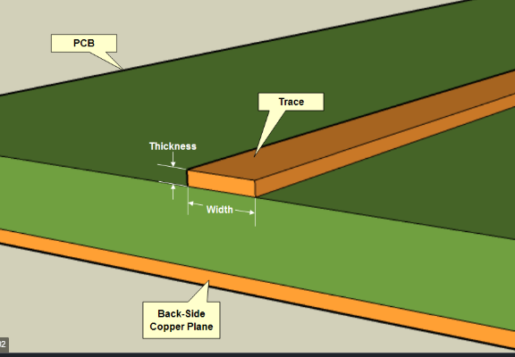
The capacitance between the signal plane and the ground plane?![]() We take the dielectric constant of teh PCB, yes dielectric as in whats in a capacitor, and then calculate the thickness of the layer and the width of the race to come up with the value we want
We take the dielectric constant of teh PCB, yes dielectric as in whats in a capacitor, and then calculate the thickness of the layer and the width of the race to come up with the value we want![]() @siddacious it's just a wire, in the absence of anything to "capacitate" against, that's an inductor
@siddacious it's just a wire, in the absence of anything to "capacitate" against, that's an inductor![]() Ted, chime in if you have something about impedance and then PCB as this is important concept
Ted, chime in if you have something about impedance and then PCB as this is important concept![]() Our biggest tool for setting the impedance of a trace is to space it away from a reference (ground) plane by a consistent amount and use the PCB material as a dielectric, I.E. we make a capacitor. Once we set the distance between plane and signal and we know the dielectric constant for PCB ( approx. 4 for FR4) we calculate the tracewidth to create the right amount of cap.
Our biggest tool for setting the impedance of a trace is to space it away from a reference (ground) plane by a consistent amount and use the PCB material as a dielectric, I.E. we make a capacitor. Once we set the distance between plane and signal and we know the dielectric constant for PCB ( approx. 4 for FR4) we calculate the tracewidth to create the right amount of cap.![]() @Ted Yapo ah, ok. That makes sense well enough, thanks
@Ted Yapo ah, ok. That makes sense well enough, thanks![]() i.e. black magic
i.e. black magic![]()
![]()
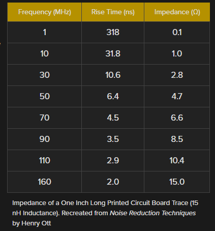
![]() So speaking of inductance, here is a chart
So speaking of inductance, here is a chart![]() 15 ohms!!!! ACK
15 ohms!!!! ACK![]() [re: previous posted picture--sorry I'm slow] I get the intuition of a 'fast, local' source of current supplied by a decoupling cap. That LC diagram also looks like a lowpass filter--is that another useful way to think about it--filtering out HF noise on the powerline?
[re: previous posted picture--sorry I'm slow] I get the intuition of a 'fast, local' source of current supplied by a decoupling cap. That LC diagram also looks like a lowpass filter--is that another useful way to think about it--filtering out HF noise on the powerline?![]() yeah, and check out those rise times
yeah, and check out those rise times![]() The trace is just a single trace or is it over a plane ?
The trace is just a single trace or is it over a plane ?![]() So rule one, smooth impedance when possible, rule two,: match the impedance of the trace to the driver
So rule one, smooth impedance when possible, rule two,: match the impedance of the trace to the driver![]()
![]()
![]() but which frequency do we use to calculate the resistance? the capacitor would be 50 ohm just at one frequency
but which frequency do we use to calculate the resistance? the capacitor would be 50 ohm just at one frequency![]() @MatYay For controlled impedance and minimal inductance there is always a ground plane for what I am talking about
@MatYay For controlled impedance and minimal inductance there is always a ground plane for what I am talking about![]() so "controlled impedance" in the context of PCB manufacturing means that the dialectric constant of the substrate and thickness are more closely controlled in order to be able to achieve better tolerances?
so "controlled impedance" in the context of PCB manufacturing means that the dialectric constant of the substrate and thickness are more closely controlled in order to be able to achieve better tolerances?![]() ok, thx
ok, thx![]() Not getting this picture. The signal traces are between 2 ground planes?
Not getting this picture. The signal traces are between 2 ground planes?![]() @Frank Buss the awesome thing about transmission lines is that they're the same impedance at all frequencies (give or take)
@Frank Buss the awesome thing about transmission lines is that they're the same impedance at all frequencies (give or take)![]() @Dave Blundell Well first its the freqency based on the rise time of yoru chips. As someone noted,, FPGAs and other chips can have their outputs slowed down just to not make trouble if really fast is not needed
@Dave Blundell Well first its the freqency based on the rise time of yoru chips. As someone noted,, FPGAs and other chips can have their outputs slowed down just to not make trouble if really fast is not needed![]() I'm wondering what the "checkbox" at the board house buys you?
I'm wondering what the "checkbox" at the board house buys you?![]() I showed a trace with a groun above and below, sorry, let me find one for a single ground plane
I showed a trace with a groun above and below, sorry, let me find one for a single ground plane![]() most 32 bit microcontrollers also have slew rate limit as an optional feature on their gpio pins
most 32 bit microcontrollers also have slew rate limit as an optional feature on their gpio pins![]()


 I blame Google