Lutetium
-
Hack Chat Transcript, Part 3
03/11/2020 at 20:06 • 1 comment![]() It also helps to remember that not everything gets soldered.
It also helps to remember that not everything gets soldered.![]() The gold protects the vias from oxidation.
The gold protects the vias from oxidation.![]() Any tips for that "low-oxygen low-humidity environment"? How about a ziplock bag and a tiny desiccant pack? Are the better (but affordable in volume) methods to keep a PCB as usable as possible for 4 year shelf life?
Any tips for that "low-oxygen low-humidity environment"? How about a ziplock bag and a tiny desiccant pack? Are the better (but affordable in volume) methods to keep a PCB as usable as possible for 4 year shelf life?![]() I forgot the unused pads.. I usually tent vias to put silkscreen over it
I forgot the unused pads.. I usually tent vias to put silkscreen over it![]() @Paul Stoffregen Really, I'd recommend moving to "just-in-time" ordering if possible. A PCB that sits around for four years is going to absorb all sorts of environmental contaminants that are going to make soldering difficult.
@Paul Stoffregen Really, I'd recommend moving to "just-in-time" ordering if possible. A PCB that sits around for four years is going to absorb all sorts of environmental contaminants that are going to make soldering difficult.![]() @guido.giunchi That's good practice -- but not 100% successful. Moisture and whatnot can still creap through.
@guido.giunchi That's good practice -- but not 100% successful. Moisture and whatnot can still creap through.![]() @Paul Stoffregen if you have any type of vacuum sealer, thats your best bet. This is how we keep our stock boards (with a desiccant also placed inside
@Paul Stoffregen if you have any type of vacuum sealer, thats your best bet. This is how we keep our stock boards (with a desiccant also placed inside![]() @Mark J Hughes @Elijah which finish is most commonly used on the boards you build? Do most of the boards come out of your shop with ENIG finish?
@Mark J Hughes @Elijah which finish is most commonly used on the boards you build? Do most of the boards come out of your shop with ENIG finish?![]() In our fab, we have a rule that a PCB may only be left for one year in our stores. After that, it gets thrown out. People who are responsible for buying PCBs acknowledge this and plan ordering according to statistical plans.
In our fab, we have a rule that a PCB may only be left for one year in our stores. After that, it gets thrown out. People who are responsible for buying PCBs acknowledge this and plan ordering according to statistical plans.has some info on via filling at the 1398s mark.
![]()
https://www.youtube.com/watch?v=efi9IzFJ4W4&t=1398s
![]() @Evan Juras i would say HASL finish due to the fact that we specialize in quick turn-proto type orders. Most quick-turn / prototype orders are focused on saving as much money as possible
@Evan Juras i would say HASL finish due to the fact that we specialize in quick turn-proto type orders. Most quick-turn / prototype orders are focused on saving as much money as possible![]() @MS-BOSS correct, we use the same practice. 1 year storage, then we toss the boards.
@MS-BOSS correct, we use the same practice. 1 year storage, then we toss the boards.![]() @Evan Juras But it's not that much more expensive to upgrade. And it can save a bunch of hassle at Assembly.
@Evan Juras But it's not that much more expensive to upgrade. And it can save a bunch of hassle at Assembly.![]() I'm surprised to hear you say HASL. I would have thought that was too rough for most SMT.
I'm surprised to hear you say HASL. I would have thought that was too rough for most SMT.![]() @Audi McAvoy The SMT issue comes down largely to stencil gasketing.
@Audi McAvoy The SMT issue comes down largely to stencil gasketing.![]() If you have a solder-paste printer, it doesn't matter what the coplanarity of your pads is.
If you have a solder-paste printer, it doesn't matter what the coplanarity of your pads is.![]() @Audi McAvoy I would say the margin is much higher. If i were to take a walk through the shop right now, I would have to keep a close count.
@Audi McAvoy I would say the margin is much higher. If i were to take a walk through the shop right now, I would have to keep a close count.![]() Guess who's got two thumbs and a solder-paste printer?
Guess who's got two thumbs and a solder-paste printer?![]() @Mark J Hughes Ah, I have to keep remembering that not everyone is using stencils.
@Mark J Hughes Ah, I have to keep remembering that not everyone is using stencils.![]() @Audi McAvoy You can't use stencils in a quick-turn shop.
@Audi McAvoy You can't use stencils in a quick-turn shop.![]() Sadly, solder printer is too slow. Since we are making hundreds of boards daily in our own assembly line, using a printer instead of stencil is a no-go. So, for large production, you are left with stencils.
Sadly, solder printer is too slow. Since we are making hundreds of boards daily in our own assembly line, using a printer instead of stencil is a no-go. So, for large production, you are left with stencils.![]() We routinely assembly boards in 6-8 hours for many of our high-tier clients.
We routinely assembly boards in 6-8 hours for many of our high-tier clients.![]() That's from when we get the design files to when we push them out the door in our shipping department. And that includes ordering & receiving parts!
That's from when we get the design files to when we push them out the door in our shipping department. And that includes ordering & receiving parts!![]() If you need to make a stencil adjustment -- a little more paste here, a little less here, you just can't do it.
If you need to make a stencil adjustment -- a little more paste here, a little less here, you just can't do it.![]() Versus throwing the board in a solder-paste printer and hitting the "enter" key and letting the machine vision do the rest.
Versus throwing the board in a solder-paste printer and hitting the "enter" key and letting the machine vision do the rest.![]() Nice.
Nice.![]() I mean, there's a little more to it than that, but not much.
I mean, there's a little more to it than that, but not much.![]() I do recall someone mentioning time factor. Each shop will be different, but it comes down to what processes the shop has in-house vs what they will have to have done at another shop. Anything we cant do in our own shop is a quick drive away.
I do recall someone mentioning time factor. Each shop will be different, but it comes down to what processes the shop has in-house vs what they will have to have done at another shop. Anything we cant do in our own shop is a quick drive away.![]() Yeah -- we have our own teams assigned at the major distributors. They pull parts just for us.
Yeah -- we have our own teams assigned at the major distributors. They pull parts just for us.![]() @MS-BOSS -- yeah -- we specialize in prototype / MOQ 1 orders. You sound like you do large-volume. There stencils still are king.
@MS-BOSS -- yeah -- we specialize in prototype / MOQ 1 orders. You sound like you do large-volume. There stencils still are king.![]() Does finish get applied to the inside of plated vias? If so, how? How do you get the finish in those tiny holes? :)
Does finish get applied to the inside of plated vias? If so, how? How do you get the finish in those tiny holes? :)![]() Since ENIG and HASL are our main choices... we have them both in house and ready to go! I know that Silver is one of our outsourced finishes, but we can have it sent out and returned in just a few hours.
Since ENIG and HASL are our main choices... we have them both in house and ready to go! I know that Silver is one of our outsourced finishes, but we can have it sent out and returned in just a few hours.![]() @Mark J Hughes Yes, we do large volumes, but only for our internal needs. We have two or three SMT assembly lines and one solder wave machine for THTs. Not sure if we do have selective solder wave tough.
@Mark J Hughes Yes, we do large volumes, but only for our internal needs. We have two or three SMT assembly lines and one solder wave machine for THTs. Not sure if we do have selective solder wave tough.![]() @MS-BOSS -- where are you located? The States? Somewhere else?
@MS-BOSS -- where are you located? The States? Somewhere else?![]() @Evan Juras Yes, the finish is also applied inside of all plated holes that are exposed (non-tented with soldermask). We are able to plate most hole sizes in our standard tanks... but for those smaller holes (or holes above 10/1 aspect ratio) we have custom pulse plating tanks.
@Evan Juras Yes, the finish is also applied inside of all plated holes that are exposed (non-tented with soldermask). We are able to plate most hole sizes in our standard tanks... but for those smaller holes (or holes above 10/1 aspect ratio) we have custom pulse plating tanks.![]() @Mark J Hughes Czech Republic, but our company has development centers and production fabs ins everal other places on the globe, too.
@Mark J Hughes Czech Republic, but our company has development centers and production fabs ins everal other places on the globe, too.![]() @MS-BOSS Very cool. Well we are very happy to have a friend across the globe :)
@MS-BOSS Very cool. Well we are very happy to have a friend across the globe :)![]()
http://listen.shoutcast.com/zeelradio.m3u
![]() Are there any other questions we've missed due to scrolling?
Are there any other questions we've missed due to scrolling?![]() I'd also like to again plug our 100% FREE webcourse that starts at the end of the month. 50 lucky participants will get their designs fabbed / assembled / shipped for free!
I'd also like to again plug our 100% FREE webcourse that starts at the end of the month. 50 lucky participants will get their designs fabbed / assembled / shipped for free!![]()
![]()
![]() For your basic maker in his basement using a stencil. the best finish would be ENIG?
For your basic maker in his basement using a stencil. the best finish would be ENIG?![]() Yes -- Enig
Yes -- Enig![]() I don't have a basement - still ENIG?
I don't have a basement - still ENIG?![]() Oh -- and KeySight is giving away oscilloscopes in the course!
Oh -- and KeySight is giving away oscilloscopes in the course!![]() As price is probably more of concern for a hobby maker than perfection, maybe OSP could be OK, however not every fab lists this finish as their standard ability...
As price is probably more of concern for a hobby maker than perfection, maybe OSP could be OK, however not every fab lists this finish as their standard ability...![]() @Christoph -- you really should get a basement. Or perhaps a root-cellar for ENIG.
@Christoph -- you really should get a basement. Or perhaps a root-cellar for ENIG.![]() Awesome - more chances NOT to win - grumble...
Awesome - more chances NOT to win - grumble...![]() @MS-BOSS makes a good point -- but OSP is pretty fragile -- you can damage it if you don't handle the board carefully -- also very short service life.
@MS-BOSS makes a good point -- but OSP is pretty fragile -- you can damage it if you don't handle the board carefully -- also very short service life.![]() Is there anything in particular we should look for when inspecting finish on newly ordered PCBs?
Is there anything in particular we should look for when inspecting finish on newly ordered PCBs?![]() Apologies to all, I didn't want to shame you because i have a basement.
Apologies to all, I didn't want to shame you because i have a basement.![]() @Dan Maloney Why can't you win?
@Dan Maloney Why can't you win?![]() 'cause other people want to sign up?
'cause other people want to sign up?![]() Does good use of flux overcome the OSP issues in re-work sort of way?
Does good use of flux overcome the OSP issues in re-work sort of way?![]() When making PCBs in our makerspace which is located in basement of college dormitories in the "real hobby style", we usually make them using the photoprocess, then coat them in immersion silver to make them solderable for longer periods of time (it stays OK for months). Vias are then made after cleaning the boards using rivets. But that is really just for "hobby" things.
When making PCBs in our makerspace which is located in basement of college dormitories in the "real hobby style", we usually make them using the photoprocess, then coat them in immersion silver to make them solderable for longer periods of time (it stays OK for months). Vias are then made after cleaning the boards using rivets. But that is really just for "hobby" things.![]() @Andy Geppert it might. And for a maker-style project, it might not matter. But the idea is to keep the oxides from forming in the first place. Damaged OSP allows oxygen in. Flux might fix that, and it might not. I'd lean towards not. But it might not matter.
@Andy Geppert it might. And for a maker-style project, it might not matter. But the idea is to keep the oxides from forming in the first place. Damaged OSP allows oxygen in. Flux might fix that, and it might not. I'd lean towards not. But it might not matter.![]() @Mark J Hughes - Luck o' the Irish, I suppose - been entering Keysight's Wave contests for three years and still nothing. It's almost like the statistics are against me or something ;-)
@Mark J Hughes - Luck o' the Irish, I suppose - been entering Keysight's Wave contests for three years and still nothing. It's almost like the statistics are against me or something ;-)![]() @MS-BOSS -- oh look at MS-BOSS with his fancy basement ;)
@MS-BOSS -- oh look at MS-BOSS with his fancy basement ;)![]() maybe off topic - but how can a hobbyist get on an 8- or even 10-layer panel?
maybe off topic - but how can a hobbyist get on an 8- or even 10-layer panel?![]() $
$![]() that's cheating
that's cheating![]() same as everyone else :)
same as everyone else :)![]() @Christoph Not at home, unless you are a fanatic.
@Christoph Not at home, unless you are a fanatic.![]() @Dan Maloney I've entered those too! Well you can enter my contest -- I'm in charge of the giveaway. Odds should be better than 1 in 100.
@Dan Maloney I've entered those too! Well you can enter my contest -- I'm in charge of the giveaway. Odds should be better than 1 in 100.![]() OK, official time is up. Mark and Elijah probably both have to get back to work, so let's just say thanks for the chat. I'll post a transcript soon.
OK, official time is up. Mark and Elijah probably both have to get back to work, so let's just say thanks for the chat. I'll post a transcript soon.![]() Excellent chat. Super thank you!
Excellent chat. Super thank you!![]() @Christoph You want the whole panel?
@Christoph You want the whole panel?![]() @Evan Juras yes, @Christoph posted a great example of a very rough finish at the beginning of our chat. The finish looked like it had very deep grooves.... this is cause for poor solderability. Discolored spotting in the finish can also be a sign of a bad plating tank, but this should be caught by the QC department and never shipped out.You just want it to look flat, smooth and shaped well (meaning a square should be a square/ a circle should be a circle)
@Evan Juras yes, @Christoph posted a great example of a very rough finish at the beginning of our chat. The finish looked like it had very deep grooves.... this is cause for poor solderability. Discolored spotting in the finish can also be a sign of a bad plating tank, but this should be caught by the QC department and never shipped out.You just want it to look flat, smooth and shaped well (meaning a square should be a square/ a circle should be a circle)![]() Thanks Mark and Elijah!
Thanks Mark and Elijah!![]() Awesome, thank you Mark and Elijah! Very informative chat.
Awesome, thank you Mark and Elijah! Very informative chat.![]() no not a whole panel just a few 10 cm²
no not a whole panel just a few 10 cm²![]() Just order a panel through us. Unless you need it crazy fast, the costs are pretty reasonable.
Just order a panel through us. Unless you need it crazy fast, the costs are pretty reasonable.![]() +1 : Thanks Mark and Elijah!
+1 : Thanks Mark and Elijah!![]() Royal lists custom Solder mask colors in their capabilities... How custom are they and can I say "mix X for me". I'm guessing the chemistry is more complicated but what can you do?
Royal lists custom Solder mask colors in their capabilities... How custom are they and can I say "mix X for me". I'm guessing the chemistry is more complicated but what can you do?![]() Thank you @Elijah and @Mark J Hughes for your time and information.
Thank you @Elijah and @Mark J Hughes for your time and information.![]() If anyone who is interested in microwave-grade PCBs wants to know more about why nickel is not your goodfriend and why that makes ENIG and ENEPIG not that good as you might think, look here at one of my logs:
If anyone who is interested in microwave-grade PCBs wants to know more about why nickel is not your goodfriend and why that makes ENIG and ENEPIG not that good as you might think, look here at one of my logs:https://hackaday.io/project/169808-microwave-stuff-what-to-do-and-what-to-avoid/log/173571-so-you-were-told-to-use-gold-finish-on-your-microwave-projects
![]() Next week we switch gears and talk about amateur radio homebrewing:
Next week we switch gears and talk about amateur radio homebrewing:![]() @Christoph just reach out -- maybe we can pair it with another customers panel.
@Christoph just reach out -- maybe we can pair it with another customers panel.![]()
https://hackaday.io/event/169987-amateur-radio-homebrewing-hack-chat
![]() Thanks everyone, it's been fun!
Thanks everyone, it's been fun!![]() @Mark J Hughes that would be awesome!
@Mark J Hughes that would be awesome! -
Hack Chat Transcript, Part 2
03/11/2020 at 20:05 • 0 comments![]() Hi everyone!
Hi everyone!![]() Welcome Mark and Elijah! Can you start us off with a little about yourselves?
Welcome Mark and Elijah! Can you start us off with a little about yourselves?![]() Hey everyone, my name is Elijah. I’ve worked at Royal Circuit Solutions in Hollister, California for the last 6 years. I specialize in DFM/DRC here at Royal as well as “blue-printing” the manufacturing procedures for the orders that come through the shop.
Hey everyone, my name is Elijah. I’ve worked at Royal Circuit Solutions in Hollister, California for the last 6 years. I specialize in DFM/DRC here at Royal as well as “blue-printing” the manufacturing procedures for the orders that come through the shop.![]() My name is Mark and I'm also part of the team. When they don't have me digging semi-precious recyclable plastics out of the dumpster, they let me research, write, speak and create content for electrical engineers.
My name is Mark and I'm also part of the team. When they don't have me digging semi-precious recyclable plastics out of the dumpster, they let me research, write, speak and create content for electrical engineers.![]() I also pay for my own business cards -- so you'll see my job description range from "3rd-shift Hypnotist" to "Research Director".
I also pay for my own business cards -- so you'll see my job description range from "3rd-shift Hypnotist" to "Research Director".![]() What questions can we provide answers for today?
What questions can we provide answers for today?![]() Business cards... made from PCBs I assume? ;)
Business cards... made from PCBs I assume? ;)![]() And just a quick disclaimer, I make no guarantees that any particular answer is appropriate for any particular question.
And just a quick disclaimer, I make no guarantees that any particular answer is appropriate for any particular question.![]() @Andy Geppert Oddly enough no. They end up being too thick to carry around in large volumes.
@Andy Geppert Oddly enough no. They end up being too thick to carry around in large volumes.![]() YES! We are here to help you guys out with choosing a finish, or just help add to your knowledge of PCB finishes
YES! We are here to help you guys out with choosing a finish, or just help add to your knowledge of PCB finishes![]() Even if made 0.6 mm thick or so?
Even if made 0.6 mm thick or so?![]() I like travelling with enough that if I ever see a "business card sweepstakes" to win something that not only is my chance of winning statistically likely, but it becomes a mathematical certainty.
I like travelling with enough that if I ever see a "business card sweepstakes" to win something that not only is my chance of winning statistically likely, but it becomes a mathematical certainty.![]() Although we do see PCB business cards being ordered a few times in our shop!
Although we do see PCB business cards being ordered a few times in our shop!![]() Choosing finishes is top of my list of "things I'd like to learn about." Understanding cost/time trade-offs.
Choosing finishes is top of my list of "things I'd like to learn about." Understanding cost/time trade-offs.![]() What is the basic finish and pro/cons?
What is the basic finish and pro/cons?![]() There are more things to consider, if one goes beyond 1 GHz with their PCBs. Anyone interested in that?
There are more things to consider, if one goes beyond 1 GHz with their PCBs. Anyone interested in that?![]() @MS-BOSS Yeah -- if you make them too thin it gets hard to drill and route. -- 0.6mm is still too thick for a business card.
@MS-BOSS Yeah -- if you make them too thin it gets hard to drill and route. -- 0.6mm is still too thick for a business card.![]() I'm interested in 1 GHz+ !
I'm interested in 1 GHz+ !![]() My boards are all well within 1GHz, but I'm interested in hearing about it just to learn more.
My boards are all well within 1GHz, but I'm interested in hearing about it just to learn more.![]() hey @Andy Geppert then thats what we will do! Seeing if we have any questions off that bat, then we will get into spilling out the knowledge
hey @Andy Geppert then thats what we will do! Seeing if we have any questions off that bat, then we will get into spilling out the knowledge![]() Super easy question. What does "finishes" mean? Are we talking about solder mask here?
Super easy question. What does "finishes" mean? Are we talking about solder mask here?![]() @Elijah is going to copy/paste some stuff in as an overview and then we'll hit the questions.
@Elijah is going to copy/paste some stuff in as an overview and then we'll hit the questions.![]() Alrighty guys, im going to start dropping info here while mark answers your questions
Alrighty guys, im going to start dropping info here while mark answers your questions![]() So to start off.....When selecting your PCB finish, the main concern should be connectivity between the PCB and your components. Are you trying to temporarily protect the copper from oxidation (lower end finishes), or are we establishing the foundation of the connection with higher end finishes?
So to start off.....When selecting your PCB finish, the main concern should be connectivity between the PCB and your components. Are you trying to temporarily protect the copper from oxidation (lower end finishes), or are we establishing the foundation of the connection with higher end finishes?As you select higher end finishes, the assembly process should become easier. The solder yield and the shelf life will also increase.
![]() I should have asked first, is there a spreadsheet somewhere for entering questions?
I should have asked first, is there a spreadsheet somewhere for entering questions?![]() @MS-BOSS @guido.giunchi Let's revisit high speed after Elijah's quick once-over.
@MS-BOSS @guido.giunchi Let's revisit high speed after Elijah's quick once-over.![]() @Audi McAvoy - Nope, just shoot out the questions right here
@Audi McAvoy - Nope, just shoot out the questions right here![]() We will be covering these main finishes, but we are open to helping you however we can:
We will be covering these main finishes, but we are open to helping you however we can:![]() OSP, HASL/HASL-LeadFree, Immersion Tin (White Tin), Immersion Silver, ENIG, ENEPIG
OSP, HASL/HASL-LeadFree, Immersion Tin (White Tin), Immersion Silver, ENIG, ENEPIG![]() So the "finishes" are the last steps in PCB fabrication -- the outer layers. Most of the time that is referring to how the PCB is prepared for assembly.
So the "finishes" are the last steps in PCB fabrication -- the outer layers. Most of the time that is referring to how the PCB is prepared for assembly.![]() So lets start with HASL and HASL-LeadFree finishes:
So lets start with HASL and HASL-LeadFree finishes:![]() So it is before the solder mask?
So it is before the solder mask?![]() HASL stands for HOT AIR SOLDER LEVEL. This is the cheapest option due to it being the most common finish used in the PCB industry. A coating of molten solder is applied to the exposed copper, then the excess solder is removed with a hot air “knife”.
HASL stands for HOT AIR SOLDER LEVEL. This is the cheapest option due to it being the most common finish used in the PCB industry. A coating of molten solder is applied to the exposed copper, then the excess solder is removed with a hot air “knife”.![]() Copper is a great material to work with -- but, like a lot of materials, it oxidizes quickly. So you have to do something to prevent the oxidation.
Copper is a great material to work with -- but, like a lot of materials, it oxidizes quickly. So you have to do something to prevent the oxidation.![]() Some are before, some are after depending on the procedure
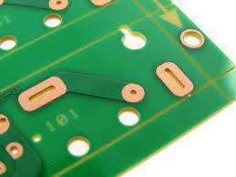
Some are before, some are after depending on the procedure![]() @Mark J Hughes do you have a picture of a PCB before and after finish is applied to make it clearer for @Audi McAvoy (and myself?)
@Mark J Hughes do you have a picture of a PCB before and after finish is applied to make it clearer for @Audi McAvoy (and myself?)![]() Assembly is the process of "soldering" parts on the board.
Assembly is the process of "soldering" parts on the board.![]()
![]()
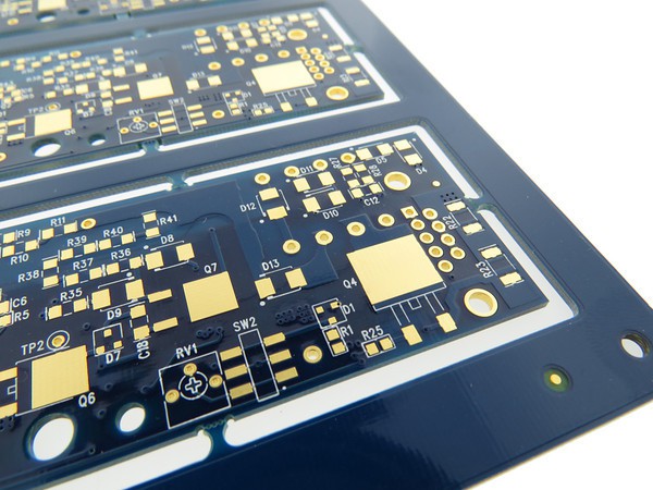
![]() here is bare copper (no finish has been applied yet
here is bare copper (no finish has been applied yet![]() And the solder-resist layer forces the solder to stay put
And the solder-resist layer forces the solder to stay put![]()
![]()
![]() and here is a board with ENIG finish applied
and here is a board with ENIG finish applied![]() I can see this chat is going to get away from us quickly.
I can see this chat is going to get away from us quickly.![]() lol
lol![]() Thanks! It's okay Mark you got and Elijah got it, it usually gets like this :)
Thanks! It's okay Mark you got and Elijah got it, it usually gets like this :)![]() Ah. I never knew the finish was applied after the mask. I guess that kind of makes sense.
Ah. I never knew the finish was applied after the mask. I guess that kind of makes sense.![]() Here are the pros and cons of HASL finish:
Here are the pros and cons of HASL finish:![]() Pros: Cheapest Price option, 12+ month shelf life (considered great), handles contact fairly well, good solderability, great protection over copper, available in Lead-Free for the environmentally cautious.
Pros: Cheapest Price option, 12+ month shelf life (considered great), handles contact fairly well, good solderability, great protection over copper, available in Lead-Free for the environmentally cautious.![]() The whole point of a surface finish is to prevent oxidation before assembly.
The whole point of a surface finish is to prevent oxidation before assembly.![]() Cons: The surface is very uneven which can prevent solder paste printers from being used, high process temperatures, RoHS restrictions and environmental issues with Leaded-HASL, not wire-bondable.
Cons: The surface is very uneven which can prevent solder paste printers from being used, high process temperatures, RoHS restrictions and environmental issues with Leaded-HASL, not wire-bondable.![]() ENIG def please (and the other while you're at it)
ENIG def please (and the other while you're at it)![]() Even an oxide layer two or three atoms thick can prevent proper solder wetting and intermetallic formation.
Even an oxide layer two or three atoms thick can prevent proper solder wetting and intermetallic formation.![]() @Nicolas Tremblay Elijah is going to list several definitions off for us, including ENIG
@Nicolas Tremblay Elijah is going to list several definitions off for us, including ENIG![]() HASL is the cheapest option due to the fact that it is the most common finish used in the industry. We run it all day every day, so its the base price when considering your finish
HASL is the cheapest option due to the fact that it is the most common finish used in the industry. We run it all day every day, so its the base price when considering your finish![]() What is meant by "not wire-bondable?"
What is meant by "not wire-bondable?"![]() @Andy Gepp
@Andy Gepp![]() Next is OSP finish:
Next is OSP finish:![]() OSP Finish: (Organic Solderability Preservative)
OSP Finish: (Organic Solderability Preservative)OSP is another cheap option where a clear, thin, organic layer is applied. Its main function is really only to preserve the copper up until the assembly process. This is probably the easiest finish as far as PCB production is concerned.
![]() Pros: Easy manufacturing keeps costs low
Pros: Easy manufacturing keeps costs low![]() Cons: The clear appearance is difficult to inspect, the thin coat is sensitive to handling (should be avoided), < 6 month shelf life, not wire-bondable. The bare copper is exposed once the OSP is removed, which is subject to oxidation.
Cons: The clear appearance is difficult to inspect, the thin coat is sensitive to handling (should be avoided), < 6 month shelf life, not wire-bondable. The bare copper is exposed once the OSP is removed, which is subject to oxidation.![]() So OSP is really only used for cheap, quick turn / early proto type boards.
So OSP is really only used for cheap, quick turn / early proto type boards.![]() Next finish is Immersion Tin:
Next finish is Immersion Tin:![]() Immersion Tin:
Immersion Tin:Tin is applied through a chemical reaction, over the copper surface layer. Its works well in protecting copper from oxidation but its reaction to copper also causes it to tarnish, lowering the shelf life and performance.
![]() Pros: Lead-Free, flat surface is ideal for assembly, high reliability, cost effective.
Pros: Lead-Free, flat surface is ideal for assembly, high reliability, cost effective.![]() Cons: 3-6 month shelf life (considered low), limited rework, handling should be avoided, reaction to copper lowers its performance over time.
Cons: 3-6 month shelf life (considered low), limited rework, handling should be avoided, reaction to copper lowers its performance over time.![]() @Andy Geppert Sometimes IC Dies are put right on the board (no epoxy packaging) and gold wires are taken off the IC and put on the PCB. I believe they are ultrasonically bonded or laser welded to the surface. The gold wires, or gold-coated wires need to "bond" or mechanically/chemically connect to the pads. Then the whole thing is covered in an epoxy blob for a "blob on board" process.
@Andy Geppert Sometimes IC Dies are put right on the board (no epoxy packaging) and gold wires are taken off the IC and put on the PCB. I believe they are ultrasonically bonded or laser welded to the surface. The gold wires, or gold-coated wires need to "bond" or mechanically/chemically connect to the pads. Then the whole thing is covered in an epoxy blob for a "blob on board" process.![]() If it isn't wire-bondable, the wires from the die won't stick to the PCB.
If it isn't wire-bondable, the wires from the die won't stick to the PCB.![]() Immersion tin comes with roughly 10% cost increase
Immersion tin comes with roughly 10% cost increase![]() Next is Immersion Silver: Immersion Silver is applied through a chemical reaction over the copper surface. It is a middle ground for pricing, which is helping gain popularity in the industry. It does not react to copper like Immersion Tin, although the silver does tarnish when exposed to air. Anti-tarnish packaging must be used when handling immersion silver finish.
Next is Immersion Silver: Immersion Silver is applied through a chemical reaction over the copper surface. It is a middle ground for pricing, which is helping gain popularity in the industry. It does not react to copper like Immersion Tin, although the silver does tarnish when exposed to air. Anti-tarnish packaging must be used when handling immersion silver finish.![]() Okay -- now for the "high-speed" guys.
Okay -- now for the "high-speed" guys.![]() Pros: Excellent solderability, provides a flat surface which is ideal for assembly, aluminum wire-bondable, 6-12 month shelf life with proper storage conditions
Pros: Excellent solderability, provides a flat surface which is ideal for assembly, aluminum wire-bondable, 6-12 month shelf life with proper storage conditionsCons: Sensitive to handling (MUST be avoided), solder within 24 hours once removing from the packaging.
![]() This gets complicated.
This gets complicated.![]()
![]()
![]() Yes tipically it's ultrasonic wire bonding. Once I soldered a pad meant to be wire bonded and I had to attach a golden lead for the bonder to work
Yes tipically it's ultrasonic wire bonding. Once I soldered a pad meant to be wire bonded and I had to attach a golden lead for the bonder to work![]() Here is ENIG:Electroless Nickel Immersion Gold
Here is ENIG:Electroless Nickel Immersion Gold The initial copper layer is coated with nickel, the nickel is then coated with a thin layer of Gold. The acts as a diffusion barrier during soldering, while the gold provides excellent protection from the nickel oxidizing.
![]() Pros: Very common = price is manageable, 12+ month shelf life (excellent), excellent solderability, aluminum wire-bondable.
Pros: Very common = price is manageable, 12+ month shelf life (excellent), excellent solderability, aluminum wire-bondable.Cons: The electroless nickel can have unwanted magnetic properties, not gold wire-bondable.
![]() The surface roughness affects wettability. It also affects the dissipation of high speed signal energy into the surrounding environment.
The surface roughness affects wettability. It also affects the dissipation of high speed signal energy into the surrounding environment.![]() Last we have ENEPIG:Electroless Nickel Electroless Palladium Immersion Gold
Last we have ENEPIG:Electroless Nickel Electroless Palladium Immersion GoldSimilar to the ENIG procedure but after Nickel, a layer of electroless palladium is added. Then gold is applied on top. The palladium acts as additional protection to prevent copper diffusion to the surface.
Pros: Superior solderability, palladium provides additional protection, gold wire-bondable, flat surface, 12+ month shelf life.
Cons: Palladium causes a weaker bond with tin/lead solders.
![]() So there is the basic info, how can we help?
So there is the basic info, how can we help?![]() So you've got to find the right balance of "roughness" to allow the solder to wet, but not too rough so that you're not dissipating your energy into the environment.
So you've got to find the right balance of "roughness" to allow the solder to wet, but not too rough so that you're not dissipating your energy into the environment.![]() And any questions asked while we were typing all that were probably lost. So ask again.
And any questions asked while we were typing all that were probably lost. So ask again.![]() Or followups.
Or followups.![]() How does the coplanarity of OSP and Immersion Tin compare to ENIG?
How does the coplanarity of OSP and Immersion Tin compare to ENIG?![]() What is your "to go" choice for general purpose? Prototype or finished products
What is your "to go" choice for general purpose? Prototype or finished products![]() @Elijah how much more expensive is ENIG than HASL?
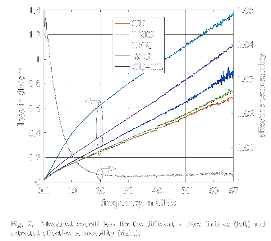
@Elijah how much more expensive is ENIG than HASL?![]() There is one problem with finishes containing nickel like ENIG and ENEPIG, since nickel is ferromagnetic. Its material resonance happens between 2 and 3 Ghz, no matter how you design the PCB. Therefore it has high losses at microwave frequencies above 2 GHz.
There is one problem with finishes containing nickel like ENIG and ENEPIG, since nickel is ferromagnetic. Its material resonance happens between 2 and 3 Ghz, no matter how you design the PCB. Therefore it has high losses at microwave frequencies above 2 GHz.![]() @Audi McAvoy Immersion Tin is the worst for coplanarity -- so you should really use a solder-paste printer during assembly, as opposed to a solder stencil. ENIG and OSP are flat -- OSP is prone to handling damage and a shorter shelf life.
@Audi McAvoy Immersion Tin is the worst for coplanarity -- so you should really use a solder-paste printer during assembly, as opposed to a solder stencil. ENIG and OSP are flat -- OSP is prone to handling damage and a shorter shelf life.![]() I'm curious about maximizing shelf life for "maker" (or rapid prototyping) circuit boards, where the PCB has already gone through 1 or 2 reflow steps to solder SMT part. Then it sits on a shelf for months, or even years, before a user hand solders wires or through hole parts. What can be done to maximize the solderability if a maker buys the PCB, leaves it in a box of parts for 4 years, then tries to use for it for project?
I'm curious about maximizing shelf life for "maker" (or rapid prototyping) circuit boards, where the PCB has already gone through 1 or 2 reflow steps to solder SMT part. Then it sits on a shelf for months, or even years, before a user hand solders wires or through hole parts. What can be done to maximize the solderability if a maker buys the PCB, leaves it in a box of parts for 4 years, then tries to use for it for project?![]() HASL or HASL Lead Free are solid options for "general purpose" PCBs. They are highly reliable. For your final product, you might want to consider ENIG for long term reliability
HASL or HASL Lead Free are solid options for "general purpose" PCBs. They are highly reliable. For your final product, you might want to consider ENIG for long term reliability![]() @guido.giunchi That depends on your assembly process. If you are hand soldering, go HASL. If you are using stencils, do not use HASL.
@guido.giunchi That depends on your assembly process. If you are hand soldering, go HASL. If you are using stencils, do not use HASL.![]() @guido
@guido![]() @guido.giunchi solder-stencil applications really require a high-coplanarity finish -- so use ENIG or ENEPIG. if your assembly house has a solder-paste printer (think ink-jet printer) you can use HASL and save some coin.
@guido.giunchi solder-stencil applications really require a high-coplanarity finish -- so use ENIG or ENEPIG. if your assembly house has a solder-paste printer (think ink-jet printer) you can use HASL and save some coin.![]() So to answer your question -- it depends on the capabilities of your assembly house and the assembly process.
So to answer your question -- it depends on the capabilities of your assembly house and the assembly process.![]() Thank you!
Thank you!![]() If the assembly house is my basement, using a solder stencil, ENIG would probably be best?
If the assembly house is my basement, using a solder stencil, ENIG would probably be best?![]() @MS-BOSS Thanks for that!
@MS-BOSS Thanks for that!![]() @Evan Juras HASL is considered the "base price" in the industry. Your starting quote will almost always include HASL finish. ENIG comes with roughly a 10% price adder
@Evan Juras HASL is considered the "base price" in the industry. Your starting quote will almost always include HASL finish. ENIG comes with roughly a 10% price adder![]()
![]()
![]() This diagram could help show the high losses of ENIG.
This diagram could help show the high losses of ENIG.![]() Why does ENIG guarantee long term reliability? Once it's soldered it doesn't matter much.. Right?
Why does ENIG guarantee long term reliability? Once it's soldered it doesn't matter much.. Right?![]() @Paul Stoffregen There's no great answer to your question. That's going to end badly either way. The best hope is to place it in a low-oxygen low-humidity environment and uses a fiberglass brush to rescrub the pads as well as copius amounts of flux.
@Paul Stoffregen There's no great answer to your question. That's going to end badly either way. The best hope is to place it in a low-oxygen low-humidity environment and uses a fiberglass brush to rescrub the pads as well as copius amounts of flux.![]() graph changes from unreadable to pretty good when I hover my mouse over it (in case any else is squinting trying to read it)
graph changes from unreadable to pretty good when I hover my mouse over it (in case any else is squinting trying to read it)![]() @Paul Stoffregen Sorry, I didn't know that transparency in images is broken in chat.
@Paul Stoffregen Sorry, I didn't know that transparency in images is broken in chat.![]() just click to open it and it's shown with a dark background - worked well for me
just click to open it and it's shown with a dark background - worked well for me![]() @guido.giunchi What are you referring to? One part is it helps prevent oxidation and corrosion during storage.
@guido.giunchi What are you referring to? One part is it helps prevent oxidation and corrosion during storage.Hack Chat Transcript, Part 1 03/11/2020 at 20:03 • 0 comments
@Christoph Post 'em. We'll try to get to them if we see them.
![]() @Christoph Or I mean, ask now.
@Christoph Or I mean, ask now.![]() I'm doing some other work but I have the chat window open.
I'm doing some other work but I have the chat window open.![]() Hi @Elijah
Hi @Elijah![]() I think we're overachievers.
I think we're overachievers.![]() Im always early, i usually have some type of log-in issue. But it looks like im ok today!
Im always early, i usually have some type of log-in issue. But it looks like im ok today!![]() Woohoo! Only because you logged in early.
Woohoo! Only because you logged in early.![]() Exactly!
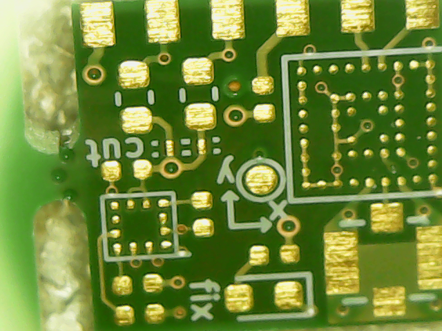
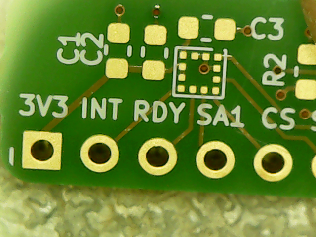
Exactly!![]() My question would be: what should an ENIG finish look like to be considered acceptable? I've had two boards with different ENIG quality - one soldered fine, the other failed. "ok" should be somewhere in between. I have pictures, too
My question would be: what should an ENIG finish look like to be considered acceptable? I've had two boards with different ENIG quality - one soldered fine, the other failed. "ok" should be somewhere in between. I have pictures, too![]() I believe that ENIG is covered under IPC-4552
I believe that ENIG is covered under IPC-4552![]() That's the standard that says what's acceptable and what's not.
That's the standard that says what's acceptable and what's not.![]() The problem is two-fold.
The problem is two-fold.![]() One, it's not all that wettable -- which means that the solder tends to ball up rather than spread out over the surface.
One, it's not all that wettable -- which means that the solder tends to ball up rather than spread out over the surface.![]() Secondly, if the coating is too thick, the intermetallics might not form, which relates to wettability, but also to reliability.
Secondly, if the coating is too thick, the intermetallics might not form, which relates to wettability, but also to reliability.![]() Even if it wets, without intermetallic formation at the interfacial layers, your parts will start to fall off the board during thermal cycling.
Even if it wets, without intermetallic formation at the interfacial layers, your parts will start to fall off the board during thermal cycling.![]() Upload the photos and we'll take a look.
Upload the photos and we'll take a look.![]()
![]()
![]()
![]()
![]() Can you show me a less blurry image of number 1?
Can you show me a less blurry image of number 1?![]() Also -- do you have pictures of these boards with soldered components on them?
Also -- do you have pictures of these boards with soldered components on them?![]() I'll try - the thing is the kids aren't in bed yet and tend to cause some trouble when I get out the good stuff
I'll try - the thing is the kids aren't in bed yet and tend to cause some trouble when I get out the good stuff![]() Ah.
Ah.![]() Well I'll just riff a little until then.
Well I'll just riff a little until then.![]()
![]()
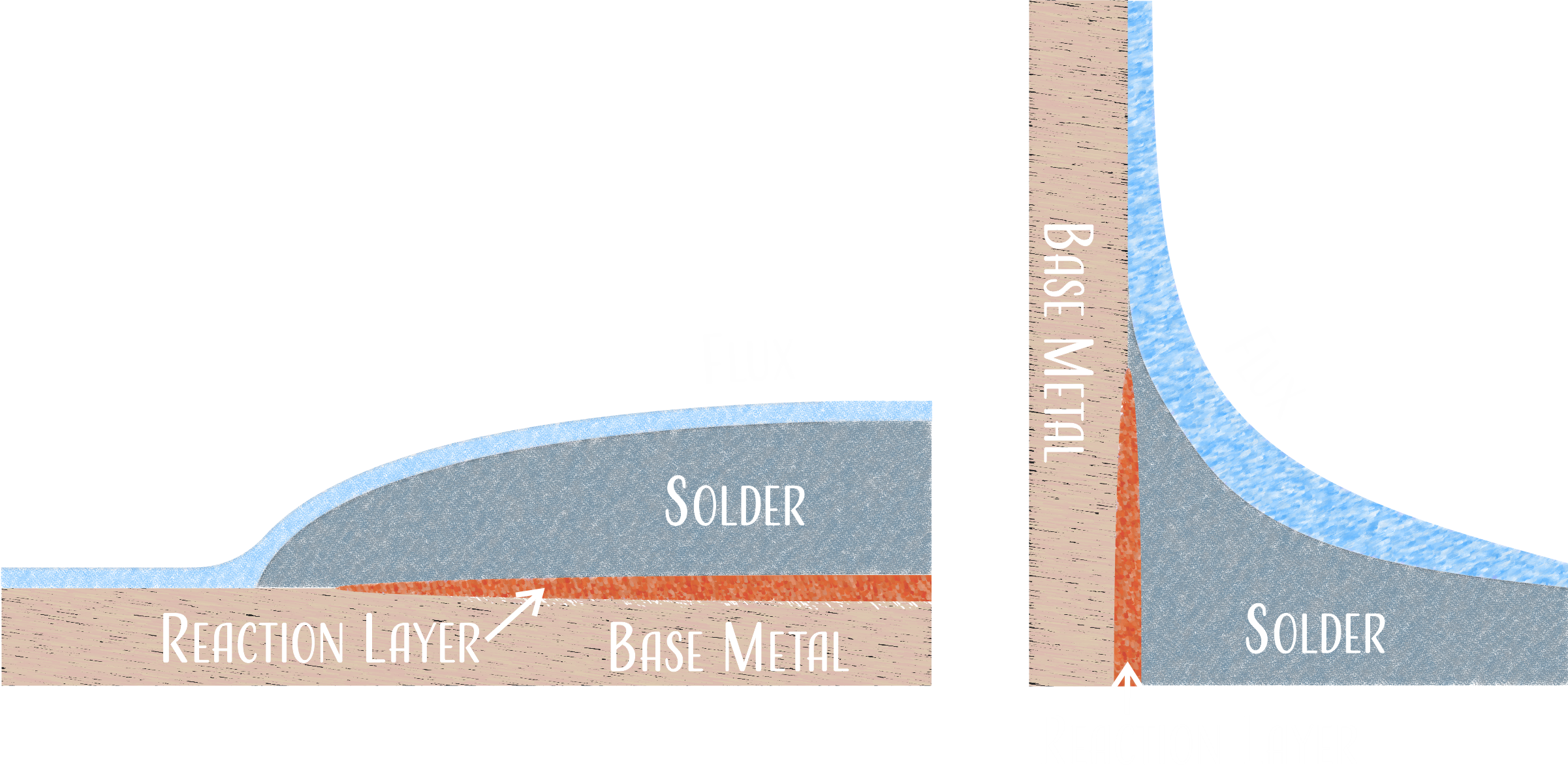
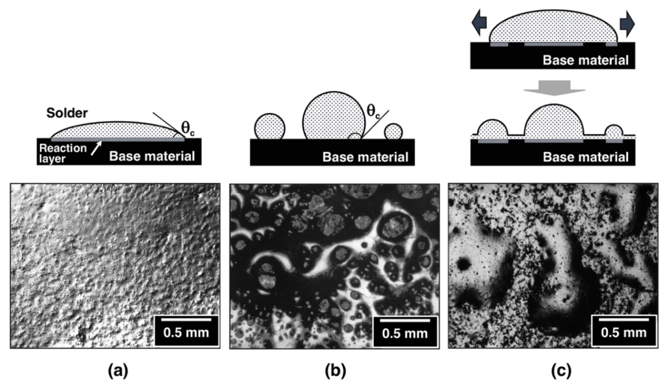
![]() When solder-paste is heated, the first thing that melts is the flux. It spreads out over the surface in a process called "wetting"
When solder-paste is heated, the first thing that melts is the flux. It spreads out over the surface in a process called "wetting"![]()
![]()
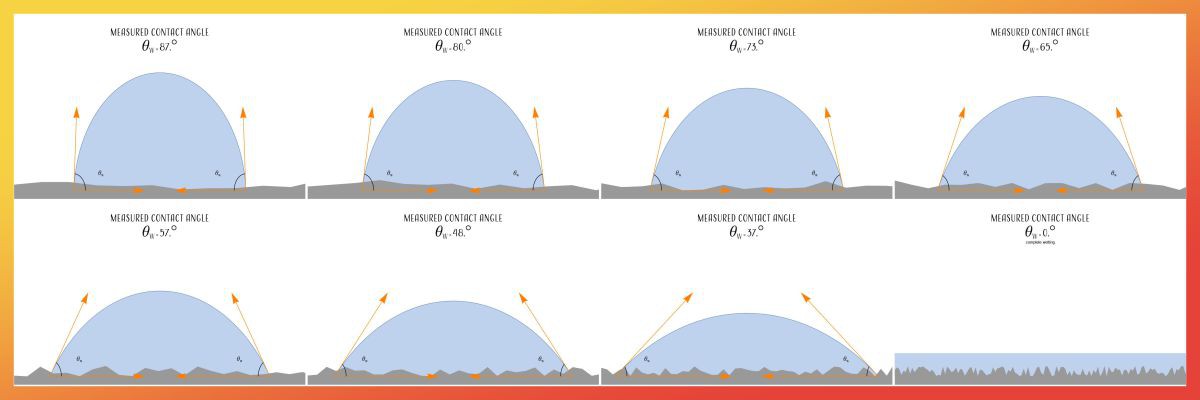
![]() Wetting is determined by the adhesive and cohesive forces between a liquid and its surroundings.
Wetting is determined by the adhesive and cohesive forces between a liquid and its surroundings.![]() The surface roughness comes into play too.
The surface roughness comes into play too.![]() Anyways -- the first thing that melts is the flux.
Anyways -- the first thing that melts is the flux.![]() It spreads out over a surface and chemically de-oxidizes is.
It spreads out over a surface and chemically de-oxidizes is.![]() does the dispensed paste blob get flatter as the flux melts or will it stay in shape?
does the dispensed paste blob get flatter as the flux melts or will it stay in shape?![]() Then at a slightly higher temperature, the solder metal melts and begins to flow over the surface.
Then at a slightly higher temperature, the solder metal melts and begins to flow over the surface.![]() (actually I can answer that myself by recalling what I see when I solder on a hot plate - it gets flatter)
(actually I can answer that myself by recalling what I see when I solder on a hot plate - it gets flatter)![]() It's also bad if the solder dissolves enough of the gold so that the joint then comes into physical contact with the nickel layer. This cannot happen during normal reflow process, but can be done during manual soldering...
It's also bad if the solder dissolves enough of the gold so that the joint then comes into physical contact with the nickel layer. This cannot happen during normal reflow process, but can be done during manual soldering...![]() The "blob" will move along metal surfaces until it is stopped by Solder-Resist.
The "blob" will move along metal surfaces until it is stopped by Solder-Resist.![]() So, as the solder becomes liquid, it begins to react with the other metals present. Let me see if I can grab a picture.
So, as the solder becomes liquid, it begins to react with the other metals present. Let me see if I can grab a picture.![]()
![]()
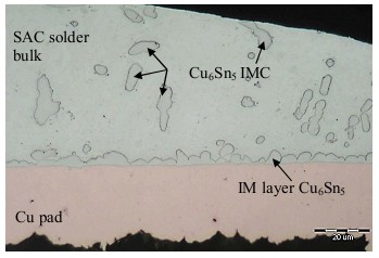
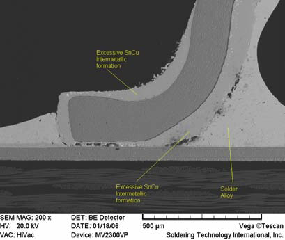
![]() At the reaction layer -- Intermetallics form -- these are essentially metal crystals that behave like pure metals.
At the reaction layer -- Intermetallics form -- these are essentially metal crystals that behave like pure metals.![]()
![]()
![]() If the intermetallic layers get too thick (pictured above) or large crystals form in the bulk of the solder, the solder joint can fail over time.
If the intermetallic layers get too thick (pictured above) or large crystals form in the bulk of the solder, the solder joint can fail over time.![]() Now you said that the boards didn't solder well.
Now you said that the boards didn't solder well.![]() That could be a fabrication issue, that could be an assembly issue.
That could be a fabrication issue, that could be an assembly issue.![]() one did solder well - the one with the smoother finish
one did solder well - the one with the smoother finish![]() From what I saw in the first picture you sent me sure does look like a fabrication issue.
From what I saw in the first picture you sent me sure does look like a fabrication issue.![]() The surface roughness appeared to be crazy-rough. Which means the solder cannot properly spread over the surface in a process called "wetting".
The surface roughness appeared to be crazy-rough. Which means the solder cannot properly spread over the surface in a process called "wetting".![]()
![]()
![]() The crystal size does affect solderability and is the reason why hard gold is so difficult to solder...
The crystal size does affect solderability and is the reason why hard gold is so difficult to solder...![]() I wanted to see a clearer image before I went down this route.
I wanted to see a clearer image before I went down this route.![]() But if the surface is too smooth, the solder will tend to ball up, or non-wet.
But if the surface is too smooth, the solder will tend to ball up, or non-wet.![]() I might be able to throw a better picture into chat later - we'll see
I might be able to throw a better picture into chat later - we'll see![]() So a tiny bit of roughness (like on the micron scale) is good.
So a tiny bit of roughness (like on the micron scale) is good.![]() But when you have large undulations like what appears in that picture, all bets are off.
But when you have large undulations like what appears in that picture, all bets are off.![]() Solder pads are meant to be largely planar shapes.
Solder pads are meant to be largely planar shapes.![]() undulations on the 10^-4 & 10^-5 range are a fabrication mess up.
undulations on the 10^-4 & 10^-5 range are a fabrication mess up.![]() the pads also seemed to be slightly "spherical" which is also visible on the first picture
the pads also seemed to be slightly "spherical" which is also visible on the first picture![]() @Elijah take a look at @Christoph 's first picture he shared.
@Elijah take a look at @Christoph 's first picture he shared.![]() Elijah has more fab experience than I do. I'm a bit curious as to what caused the striations. It seems like the mistake happened at the electroless nickel deposition step.
Elijah has more fab experience than I do. I'm a bit curious as to what caused the striations. It seems like the mistake happened at the electroless nickel deposition step.![]() But there's a chance it happened when they sanded the board, before they ever put the nickel down.
But there's a chance it happened when they sanded the board, before they ever put the nickel down.![]() And that's what I'm guessing. But I'll take @Elijah word over mine.
And that's what I'm guessing. But I'll take @Elijah word over mine.![]() He might not be on at the moment -- we're not scheduled for another few minutes.
He might not be on at the moment -- we're not scheduled for another few minutes.![]() yut, half an hour to go nd I kinda feel bad for starting the discussion early
yut, half an hour to go nd I kinda feel bad for starting the discussion early![]() Okay -- I'm going to go out on a limb and say it happened after the copper plating and before the electroless nickel.
Okay -- I'm going to go out on a limb and say it happened after the copper plating and before the electroless nickel.![]() The copper should be chemically cleaned -- but some processors put the panels through a "scrub-brush" process first. Basically a conveyor with a spinning wheel above it.
The copper should be chemically cleaned -- but some processors put the panels through a "scrub-brush" process first. Basically a conveyor with a spinning wheel above it.![]() If I had to guess -- and this is a big guess, with lots of assumptions.
If I had to guess -- and this is a big guess, with lots of assumptions.![]() Whatever board went through before yours was thinner -- and they forgot to readjust the height of the machine before board one went through.
Whatever board went through before yours was thinner -- and they forgot to readjust the height of the machine before board one went through.![]() So it "scrubbed" too hard.
So it "scrubbed" too hard.![]() Then they applied the electroless nickel
Then they applied the electroless nickel![]() And then the gold.
And then the gold.![]() The board should never have made it through QC.
The board should never have made it through QC.![]() Should never have even had the gold applied.
Should never have even had the gold applied.![]() @Elijah if you're there buddy, jump in. I'm just making things up at this point.
@Elijah if you're there buddy, jump in. I'm just making things up at this point.![]() Essentially though -- if you ever see a surface finish that is that bad -- you should be able to RMA the boards back to your supplier.
Essentially though -- if you ever see a surface finish that is that bad -- you should be able to RMA the boards back to your supplier.![]() Hey Mark, sorry! let me read whats going on. I was getting a few things finished before we start
Hey Mark, sorry! let me read whats going on. I was getting a few things finished before we start![]() No worries -- @Christoph has a ENIG board with bad surface finish -- see his post a few pages above. Look at the first picture.
No worries -- @Christoph has a ENIG board with bad surface finish -- see his post a few pages above. Look at the first picture.![]() What do you think happened?
What do you think happened?![]() And feel free to disagree with me. I was making huge leaps of the imagination.
And feel free to disagree with me. I was making huge leaps of the imagination.![]() if you can't scroll up that far I can PM the picture to one of you
if you can't scroll up that far I can PM the picture to one of you![]() I was about to tell him his interlocking framastan joint failed.
I was about to tell him his interlocking framastan joint failed.![]() @Christoph its a little hard to tell. We would have to cross-section the board to give a solid answer. But from the naked eye, the deep parallel grooves make me think that the copper was scrubbed far too aggressive before the gold was added
@Christoph its a little hard to tell. We would have to cross-section the board to give a solid answer. But from the naked eye, the deep parallel grooves make me think that the copper was scrubbed far too aggressive before the gold was added![]() And you are right on with that causing the solderability issues @Mark J Hughes
And you are right on with that causing the solderability issues @Mark J Hughes![]() sounds pausible
sounds pausible![]() @Elijah Whew! I guessed that too! Well, even blind squirrels find nuts and all that.
@Elijah Whew! I guessed that too! Well, even blind squirrels find nuts and all that.![]() @Christoph take that picture and go back to your fabrication and complain.
@Christoph take that picture and go back to your fabrication and complain.![]() Do you mind sharing who you used?
Do you mind sharing who you used?![]() @Christoph were both board manufactured at the same shop?
@Christoph were both board manufactured at the same shop?![]() that was aisler (or rather the board house they use). happened only once and I later received good boards again
that was aisler (or rather the board house they use). happened only once and I later received good boards again![]() they haven#t commented on that one bad case though
they haven#t commented on that one bad case though![]() They might have more than one board shop they partner with.
They might have more than one board shop they partner with.![]() and yes, Mark is right. That quality is unacceptable.
and yes, Mark is right. That quality is unacceptable.![]() thank you very much! I have to leave for a while but I'll surely get back later
thank you very much! I have to leave for a while but I'll surely get back later![]() Yeah they usually use multiple board shops. I am not familiar with Aisler but many brokers often use a "get what you pay for" price point. If you paid a fair price, definitely get a remake!
Yeah they usually use multiple board shops. I am not familiar with Aisler but many brokers often use a "get what you pay for" price point. If you paid a fair price, definitely get a remake!![]() So, quite a bit of "preamble" discussion here, which is great. I'll try to capture all of it for the transcript, which I'll post publically after the chat. We'll get started with the "official" chat in about 10 minutes.
So, quite a bit of "preamble" discussion here, which is great. I'll try to capture all of it for the transcript, which I'll post publically after the chat. We'll get started with the "official" chat in about 10 minutes.![]() And welcome Elijah and Mark!
And welcome Elijah and Mark!![]() Hey @Dan Maloney thanks for having us!
Hey @Dan Maloney thanks for having us!![]() Thanks @Dan Maloney -- hey would it be appropriate to promote our PCB design course? Or is this not the forum for that?
Thanks @Dan Maloney -- hey would it be appropriate to promote our PCB design course? Or is this not the forum for that?![]() What is the topic tonight?
What is the topic tonight?![]()
https://hackaday.io/event/169956-pcb-finishes-hack-chat
PCB Finishes Hack Chat
Mark Hughes and Elijah Gracia will host the Hack Chat on Wednesday, March 11, 2020 at noon Pacific Time. Time zones got you down? Here's a handy time converter! Once those traces are formed, however, there's more work to be done.
![]() @Mark J Hughes - I think it's OK to mention that. It seems like this would be a group that might want to know about that
@Mark J Hughes - I think it's OK to mention that. It seems like this would be a group that might want to know about that![]()
![]()
![]() If anyone is interested in learning the basics of Rigid PCB layout, we're starting a course at the end of the month.
If anyone is interested in learning the basics of Rigid PCB layout, we're starting a course at the end of the month.![]() If it goes well, we will extend it to Rigid-Flex design.
If it goes well, we will extend it to Rigid-Flex design.![]() And we're paying for 50 people's projects to be built (fabbed, assembled, parts & shipping)
And we're paying for 50 people's projects to be built (fabbed, assembled, parts & shipping)![]() any cost for the course?
any cost for the course?![]() 100% free
100% free![]() I mean, we kinda expect you to name your first-born "Elijah"
I mean, we kinda expect you to name your first-born "Elijah"![]() But we haven't found a lawyer willing to draw up the contracts yet.
But we haven't found a lawyer willing to draw up the contracts yet.![]() Its the least you could do!
Its the least you could do!![]() No -- the least they could do is name their first-born "Mark".
No -- the least they could do is name their first-born "Mark".![]() I mean -- that's easily 2 fewer letters.
I mean -- that's easily 2 fewer letters.![]() Sorry, he's already named and the paperwork would a pain to change it.
Sorry, he's already named and the paperwork would a pain to change it.![]() Hello everyone, welcome to the Hack Chat! Today we've got Mark Hughes and Elijah Gracia from Royal Circuit Solutions to talk to us about PCB finishes.
Hello everyone, welcome to the Hack Chat! Today we've got Mark Hughes and Elijah Gracia from Royal Circuit Solutions to talk to us about PCB finishes.


 Awesome - more chances NOT to win - grumble...