 danjovic
I have gathered some PCB footprints I have designed into a github repository:
https://github.com/Danjovic/PlasticBoxesPCBs
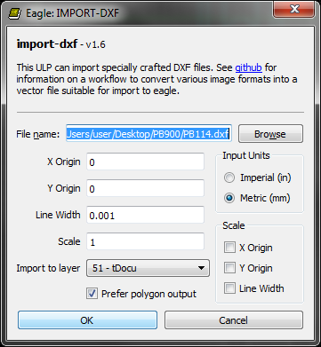
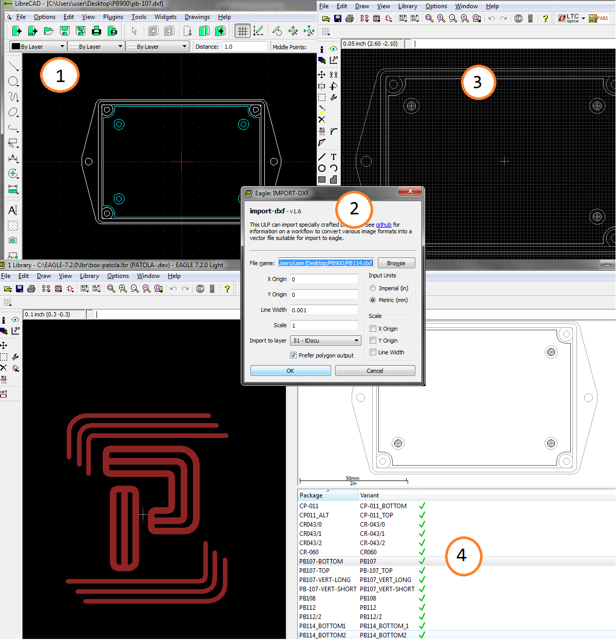
Most of the PCBs have been drawn using LibreCad and imported in Eagle using the import-dxf.ulp script.
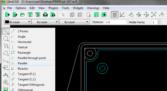
The Case outline is drawn from the manufacturer's datasheets. Then I use the (draw) Parallel line and set the distance to 1 (mm) to draw the PCB outline around the external walls and standoffs and save the file as DXF 2007.
When I run the script I left the scale at 1, and use the same scale I have drawn (mm). As most of the details I have been drawing are on the case outline I choose the tDocu layer as a primary. I usually draw on more than one layer but the importing script merges them.
After loading the DXF I change manually the layers of the board outlines to the tDimension layer. The next step is to put some holes at the desired position.
Same procedure works fine for logotypes too, and it is very nice to trace the bitmaps from Inkscape and use them on eagle, though sometimes the Inkscape generated DXFs don't work.
Discussions
Become a Hackaday.io Member
Create an account to leave a comment. Already have an account? Log In.