 danjovic
The Ninja Tap is an adapter that allows to use up to 4 joysticks per MSX port (MSX Wiki).
There is not much information available on such adapter, let alone the schematics.
I wanted to build a clone of such adapter then I have started to disassemble a driver code and translations of japanese documentation available to figure out the connections.
| Pin MSX Joystick | Function |
|---|---|
| 6 | goes to PARALLEL/!SERIAL of all 4021s |
| 8 | goes to CLOCK of all 4021s |
| 7 | receives the inverted level of signal from pin 8 (see oddity below) |
| 1 | receive the data out from the first tap port |
| 2 | receive the data out from the second tap port |
| 3 | receive the data out from the third tap port |
| 4 | receive the data out from the fourth tap port |
| 5 | is the VCC (5 Volts) |
| 9 | GND |
Protocol
The adapter uses four CD4021s to shift in the controller data from the four controllers:
disassembling the GETNIN function :
The sequence for reading the 4021s is the following
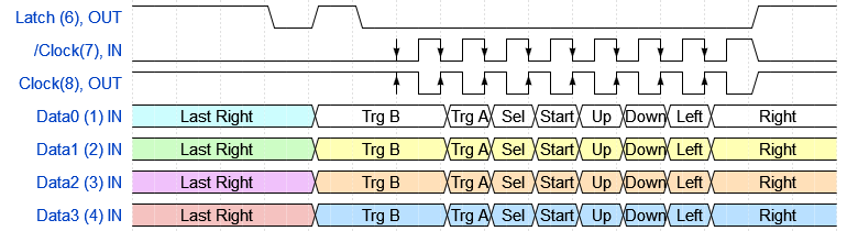
0) the sampling start with pin 8 (CLOCK = HIGH) and pin 6 (PARALLEL/!SERIAL = LOW)
- pulse (go high, then low) the PARALLEL/!SERIAL line (pin 6). That will latch the input of the keys to the 4021 internal flip flops. Notice that the CD4021 output is already loaded at the Q8 output.
- Pulse (go high, then go low) the CLOCK line (pin 8). (note: If this pin weren't initialized high, the first bit would be missed)
- shift in one data bit from TAP 1 at the UP line (pin1) into register H
- shift in one data bit from TAP 2 at the DOWN line (pin2) into register E
- shift in one data bit from TAP 3 at the LEFT line (pin3) into register D
- shift in one data bit from TAP 4 at the RIGHT line (pin4) into register C
- Repeat steps 2 through 6 for until all 8 bits are read
- Process the data.
The sequence of bits is the same used by NES controllers, being possible to make an adapter that uses 4 NES controllers with only one inverter (which makes me wonder to reuse a JoyMega adapter to create a Ninja Mega Adapter)
Oddity
The adapter was designed to be detectable by the driver, and uses the inverted state of signal at pin 8 which is applied to pin 7. The driver flips the state of pin 8 and check if inversion occurs on pin 8.
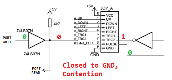
The problem is that pin 7 is an open collector and the detection routine pulls this pin down (instead of let it float ) during the detection, which means that the external inverter will have to fight (and win) against the internal 7407 open collector gate, otherwise the detection will fail.
Here's the code
;======================================
; Connection Check Sub.
; return with B=B+1 if no hardware detected
; otherwise return with B=B+4 if hardwar detected
CHECK:    CALL    PORSEL   ;
    INC    B          ; B = Max player number + 1
    AND    0C0H       ; A is state of port 15.
    OUT    (0A1H),A    ; 678=L  for both joystick ports (!)
    EX    AF,AF'      ; save state of Reg15 with all output pins low

    LD    A,14        ; select register 14
    OUT    (0A0H),A
    IN    A,(0A2H)    ; read state of joystick port
    AND    20H            ; 7=H ?   return if bit is high (!) (shouldn't be forced high, its being driven low internally )
    RET    Z           ; if return here, A = state of pin 6, and B=B+1 from the function call

    LD    A,15        ; select register 15
    OUT    (0A0H),A

    EX    AF,AF'      ; restore state of Reg15 with all output pins low
    OR    030H        ; make bits 4 and 5 high (pin 8 of both pulse pins)
    OUT    (0A1H),A    ; 8=H  for both output ports

    LD    A,14        ; select register 14
    OUT    (0A0H),A
    IN    A,(0A2H)    ; read inputs

    AND    20H            ; 7=L ? is pin 7 low
    JR    NZ,CHECK1   ; no, return with A=0

    INC    A           ; Complement bit 0 of register A (read from pin 6)
    INC    B           ; B = B+3
    INC    B
    INC    B
    RET
; No NTAP
CHECK1:    XOR    A
    RET
Discussions
Become a Hackaday.io Member
Create an account to leave a comment. Already have an account? Log In.