 Dave Collins
I received this 48K spectrum from a friend, in a mostly working state. It needed to have the membrane replaced as well as one of the 32K ram chips. Through the process of rework the DC-DC converter circuit began to fail. I believe as a result of being run at a high level for a long period of time, from an unregulated 9v supply that may have drifted slightly.
On initial inspection, I determined the 4116's must have failed as TR4 / TR5 kept blowing. I replaced them (t4 and t5) and removed the ram chips, to no avail as the transistors kept failing even with the ram chips removed. The next on the list to check was all the capacitors, I verified none were open or dead short with good ESR values ( all electrolytic were replaced first thing - and the board worked for a few hours at least). I suspected the coil was bad. At this point I started to deep dive into the circuit and read through two separate circuit descriptions trying to determine:
- why this circuit fails so much.
- why this was the most modified part of the circuit throughout the revisions.
- can this be improved uppon.
I asked my father, who was an EE from the 60's all the way to the 90's to take a look at the inverter / DC-DC circuits across the several revisions as he's vastly better at looking at analog circuits than I am. Together we determined that the DC-DC mods specifically address regulation and clamping issues in the previous versions of the circuit. While these improve supply output and manage transient voltages which feed sensitive ram chips it does not address what is conspicuously missing from ALL revisions of the 48k DC-DC circuit; 4116 bring up timing.
The 4116's and by in large the transistors inside the DC-DC circuit fail because the supply does not adhere to this note in the 4116 Datasheet:
Simply put - There is no timing mechanism beyond the R/C delay inside the circuit itself, which grants exclusively that VBB (-5v) is applied first, and removed last. Furthermore, when power is removed to turn off the system if the ground path is eliminated by disconnecting the cord completely or isolating the ground line in an improperly wired switch. There is no way to assure any sort of state on power down.
So - specifically when the 4116's fail, and they usually will, the DC-DC circuit is often damaged by an over current condition on the digital 12v rail.
So how did I improve upon the design:
Back in the 80's the most commonly used dc power supply was an unregulated 9v center negative power supply. Specifically because of this utility its obvious to me that that is the reason that iconically thrifty Sir Clive and his engineers chose this to be the supply they were to use. Moreover - not wanting to spend any amount on a switch for every unit allowed them to cut the prices even further to save Sinclair millions, by simply having the public unplug the thing or turn the switch off at the wall socket. What was needed was a minimal, cheep and dirty power circuit to create the multiple rails required for the computer and not break the bank. I think they did the best they could with the limits they had, and specifically the computers worked well enough in the day for this oversight to not matter nearly as much as it does today.
Today, we have commonplace, high quality 12V regulated power supplies that run cool and efficient and don't really break the bank. I decided to remove the DC-DC circuit in my issue 3, and use an external regulated center negative 12v power supply to power the whole computer.
This has several advantages:
- The supply is more efficient - we no longer have to "boost convert" a 12v rail using a charge pump and inverter. This reduces losses to multiple conversions going from 9v - > +5V -> +12v & -5v
- The supply is cooler - the LM7805 linear positive voltage regulator gets VERY hot especially when it is driving an inverter and several power hungry IC's like the 4116s, the NMOS z80 and the ULA. we can remove this old part and replace with a drop in switching regulator to increase efficiency and reduce heat.
- Regulated supplies are just better objectively - a regulated supply can be built to have output clamping, transient voltage suppression and over current protection. Unregulated supplies simply provide a dc voltage value from a transformer, rectifier circuit and a large output cap.
So then, how did I go about modifying my 48K for 12v? -- Below are the steps I took to make this modification. I tried where I could to use existing through holes and vias, and to keep to the silkscreen footprint where possible.
The obvious warnings and disclaimers apply here, everything is 100% at your own risk. Power circuits are dangerous and these modifications even when done correctly can damage marginal parts if a mistake is made, or no mistake at all for that matter. Additionally though the risk is low given the forces at play here working on energized power circuits while grounding yourself for ESD is dangerous and can cause injury or great harm if the computer is plugged in while working on it. I take no liability if you decide to follow this as a guide, but have tested and found it to work on my own spectrum.
Please make sure you read and understand what is happening here before you make any changes to your computer. I make a lot of assumptions about skill level and access to tools and knowledge but generally I expect:
- You know how to read schematics, and understand common electrical principles like clamping, and voltage regulation.
- you understand how to select a center negative voltage source of high quality with sufficient output characteristics for your application.
- you know how to be safe working around power circuits
- you have access to a VOM and can operate it.
- highly recommended that you have a current limited way of bringing up the power for the first time, such as a bench top power supply.
- good quality soldering tools and hand tools for making the modifications. as well as reasonable skill with a soldering iron.
CIRCUIT DIAGRAM

BILL OF MATERIALS
optional replacement components, maybe needed:
- C50, C34 - 22uF / 24V electrolytic, horizontal
- C44, C45 - 100uF / 24V electrolytic, horizontal
- R62 - 22 ohm 1/4 watt resistor (original is 15ohm, only replace if bad)
required:
- U2 - TSR 1-2450 Switching +5v regulator (or equivalent switching regulator)
- C49 (replaced with diode) - BZX55C12 - 12v .5 watt DO-35 Zener Diode
- D15 - 1N5817 1A D0-41 Schottky Rectifier diode.
- polyimide tape
- 1A 12v Regulated, center negative power supply. you should buy a UL listed supply that has over current protection at the very least, output clamping and TVS are a plus.
optional 4116 support components:
- 1x1 piece of plated through hole proto board
- short length of 24 gauge wire (red)
- short length of 24 gauge wire (black)
- short length of 30 gauge wire (red)
- D12 - 1N5817 1A D0-41 Schottky Rectifier diode.
- C100, C101 - 10uF / 16v electrolytic capacitors
- U3 - ICL7660S - cmos voltage converter
- A small 8 pin dip socket for U3.
METHOD OF PRODUCTION
With the power disconnected from the unit, and the case removed, while wearing ESD work safe wrist strap; perform the following:
UPGRADE THE REGULATOR AND CLEAR THE COIL PADS ON THE BOARD
- Replace the linear regulator and heat-sync with a switching regulator drop in replacement such as Traco Power TSR-1-2450, or equivalent. Take care to match the pin out of the LM7805 with the replacement part. When you are done you will not need the heat-sync.
- Remove the charging coil completely and clear at the very least the pads on the right.
- be careful to not damage traces on both sides of the board, highly recommend using suction and watch temperature and dwell time.
- don't be surprised if there is a small bit of glue actually under the coil here. I found some on mine.
- it is very difficult to cut this part off the board to prior to de soldering without damaging the board. avoid this method with the charge coil to prevent damaging the PCB, pads or traces.
- Bridge the right hand pads, the top corner next to the regulator and the pad in the bottom corner below (skipping the middle pin) to bring 12v directly through the 12v rail - you will want to use a larger conductor like a off clipped leg of a DO-41 Diode (this is approximately .77 mm diameter +/- .7 mm)
- done correctly you will have continuity through the outside sheath of the DC jack, and the positive pin of C50 (left side).
REMOVE AND RECONFIGURE THE DC-DC CIRCUIT
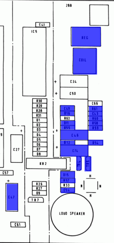
- Remove all the Highlighted components in the DC-DC circuit you can use
flush cut to clip the components from the top of the board. (except the coil which needs to be de-soldered ) - Clear the component holes for C49, C74, D12, D15, R54, and R55.
- Use forceps / tweezers to pull the legs out from top or bottom while heating with soldering iron.
- clear the through hole using a good solder wick like MG Chemicals Superwick or Gootwick.
- watch heat level and dwell time to assure this is inside the limits of connected circuits, do not apply force with the tip of the iron as the top traces are soft, and may de-laminate if too much force or heat is applied.
![]()
- Test R62 - this should be 15 ohms. if not, replace with a 15 - 22 ohm 1/4 watt resistor. mine was dead, shorted straight across.
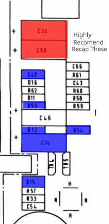
- Consider replacing C50, and C34 these are directly under the heat sync for a long time and will likely be dried out and not functioning, at this point these are still very integrated into other circuits on the board so in-circuit testing will not be precise. C50 should also be at the very least a 15v capacitor, 25v preferred. You may also wish to replace C44 and C45 (these are the 12v rail's filter capacitors).
- Replace C49 with a BZX55C12 ( 12v 1/2 Watt Zener Diode) to clamp the 12v supply line to 12v; this as a precaution - this should already be done inside the supply.
- optionally place a small piece of polyimide tape down under the diode to prevent the legs from shorting to the vias and traces in this location
- align the cathode (the side with the line) with the left pad of the footprint.
- this clamps the voltage to 12v. and will withstand currents up to 1/2 watt.
- the 4116's and the video amp total current should not exceed 300mA
- the supply regulation will need hold the voltage at 12v - so this diode is a precaution in the event a short transient occurs when plugging or unplugging the power connector, or switch transients in the case an inline switch is used (see design note below).
- Replace D12 (optional) and D15 (required) with 1N5817 Schottky Rectifier Diode.
- D12 is only needed if the optional 4116 charge pump mod is used
- D15, and D12 should follow the footprint on the board for cathode alignment.
- D12 is a smaller DO-35 footprint (though its large for that footprint range). it may be very difficult to install the larger DO-41 diode in this place. If needed, D12 in the mod is value oversized - replace with a .5A-.25A Schottkey diode in the DO-35 footprint (this will require research to assure the voltages of the circuit are met, in both directions across the diode.)
Optional Steps:
- (*OPTIONAL*) If using 4116 optional charge pump mod (see below) - install a short, red, 24 gauge solid core wire to the positive pad (left) of C74, and a red 30 gauge wire to the right pad of R55.
- (*OPTIONAL*) if using 4116 optional charge pump mod(see below) - install a short, black, solid core wire to the right pad or R54 - (this is also a good place to grab ground from if you need to tie the pad between the top H and right N jumpers -- for the EEPROM mod. )
design note:
If placing an inline switch directly into the power lead. Make sure that the positive +12V side is switched on and off and not the negative side. This helps the circuit to de-energize properly. The same goes for unplugging the computer directly. Try to avoid doing this, especially with the 4116's still installed, improperly removing even the stock circuit from ground will have the effect of potential damage to the 4116 memory chips.
Please select a 12V regulated power supply that is wired center negative. You should select a UL (or your safety board) registered supply with low ripple and over current protection at the minimum. Though other features such as TVS and output clamping would also be nice.
The issue 3/3A schematic specifies the B side is the Top of the board, as were the A side is the bottom of the board. With this in mind be aware that after the mod B22, B23 and 4A will now carry +12V after modification. 20B will be floating if the charge pump mod is not installed. Please keep this in mind when using vintage expansions with the modified computer. If any of these rails are used (mainly ram expansions), there is a high likelihood damage will occur. Certain RS232 expansions require the 12VAC line to generate signal voltage, its highly likely that this will prevent those expansions from functioning. Serial expansions that use a charge pump inverter off of the 5v line should work as long as they do not also use the 9v line. Since the modern ram expansion is 5v only, it is safe to use. As well as ram packs that do not use the +9v or the 12VAC line.
The Optional charge pump for 4116 ram chips:
I am highly recommending against putting new 4116's inside a working spectrum at this point, or leaving the old 4116's installed at all. Instead of using 4116's consider replacing the lower ram with 4164 or 41256 (requires some very simple pin bodges to the chips). These are newer, use less power and only run on 5 volts. Even the existing DC-DC converter fails to bring up, and down the 4116's in the correct way to prevent damage, so its almost a forgone conclusion that they will fail again at some point. With that being said, you were warned.
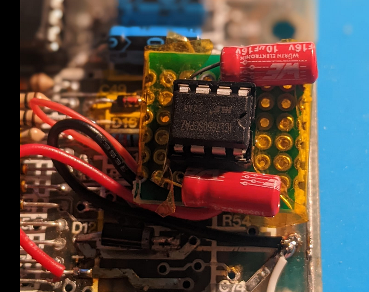
If you do want to try, you can build a very small piece, 1x1 inch, of proto-board up with this small circuit to make a -5v rail for the 4116's. This is copy paste from the ICL7660S datasheet. Essentially the 7660 is a CMOS voltage converter that can be configured for power delivery in several different ways using passive components. In this configuration it delivers a -5 volts to pin 5 by creating charging a capacitor pump circuit using 2 10uF capacitors. (I used 10uF 16v electrolytic - which seems like a good enough bit of margin here.)
be sure to tape all surfaces of the PCB so that it will not come into contact with anything below, and apply tape directly to the PCB over the whole area of the DC-DC converter to prevent the accidental punch through or the top layer traces coming into contact with the charge pump PCB.
Perform the optional steps listed above to attach short jumper wires to the main PCB. Then follow the next steps to connect the completed circuit to the wires.
- connect the large 24 gauge solid core red wire to pin 8 of the IC
- connect the large 24 gauge solid core black wire to pin 3 of the IC and, pin 3 to the positive leg of the capacitor connected to pin 5. (this capacitor appears backwards as the voltage is reverse bias IE it is less than ground reference which is zero.)
- connect the 30 gauge small red wire to pin 5 (the negative leg of the capacitor also connected there)
TESTING:
if at all possible remove the large chips and ram chips from sockets, You should set the current of a bench supply to some low value 500mA @ 12V (much lower if not using the charge pump mod and 4116's). Remember to wire the barrel plug to center negative, the Schotkey diode should prevent most miss wires -- but depending on if there are issues in the rest of the computer its not a hard and fast. Verify the voltages are correct at each of the rails. If the supply goes into current limit right away or the voltage drops check for shorts and possibly clip the 12v leg mid way on the 4116's to see if the problem goes away - you can always just put a blob of solder back on each pin you cut to put it back together. if any of the 4116's are bad - completely replace them with 4164 or 41256 (or a modern replacement) it is only a matter of time. If any of the 4116's are hot to the touch remove the power and remove that chip from the board.
YOU SHOULD HAVE:
The total current of the circuit very well may not exceed 500mA - My ula had keyboard issues and needed to be replaced with a vLA-82 this significantly reduces the operating current of the computer.
+12v on the left hand side of C50.
+5v on the left hand side of C34
-5v on pin 1 of any 4116 socket or chip (if using charge pump mod).
slightly lower than +12v on pin 8 of a 4116 socket. (there is a slight drop through the diode)
Re-socket all chips and do a final test verifying the video works:
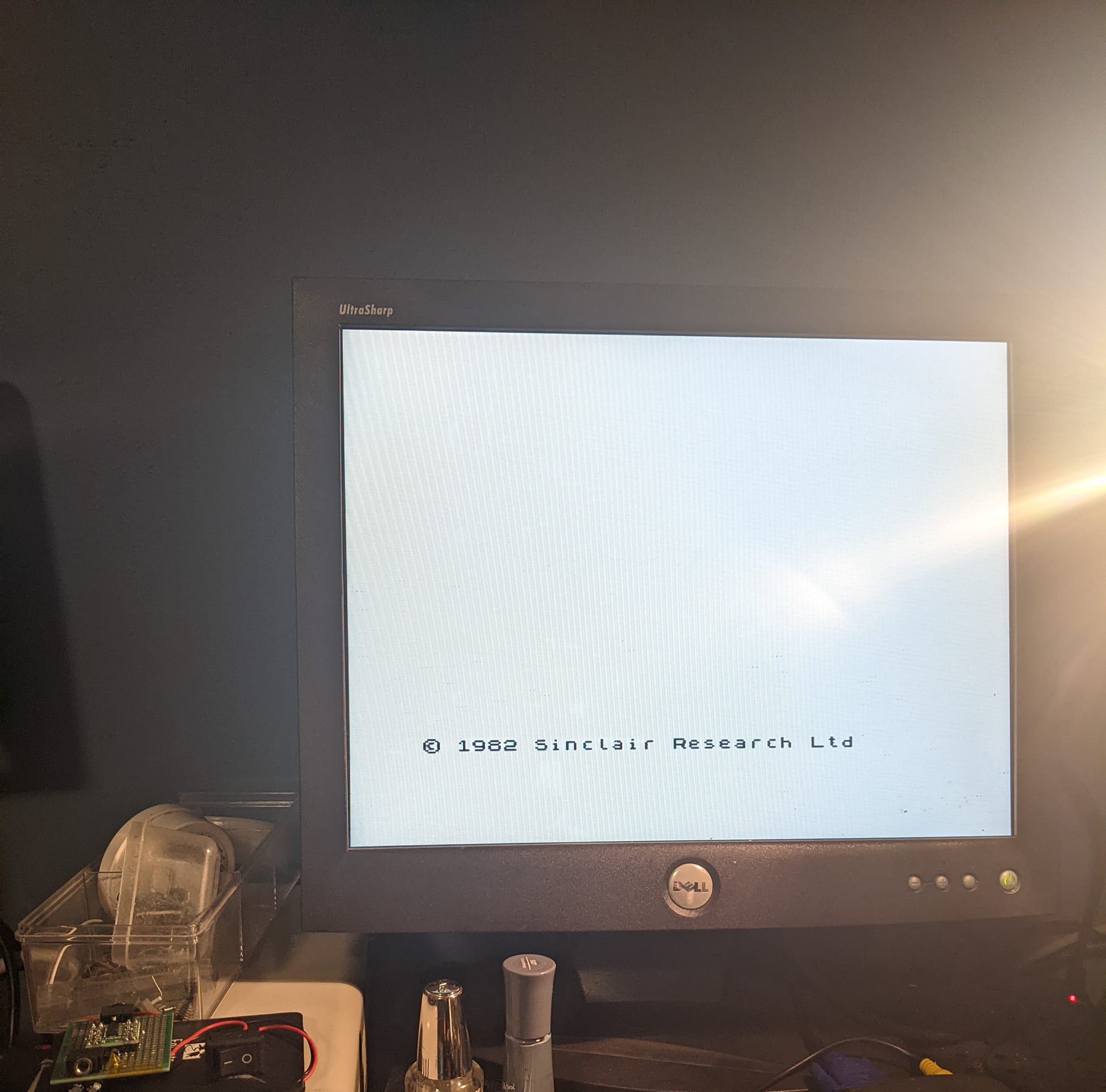
if everything is correct, you should have a working spectrum with a much more stable power supply that should last for years to come.
I hope you've enjoyed this little foray into modifying power circuits on vintage tech. What are your thoughts on these modifications? Would you have done something differently? Please drop a line below and let me know!
Discussions
Become a Hackaday.io Member
Create an account to leave a comment. Already have an account? Log In.