 Dave Collins
 Yann Guidon / YGDES
-
GPL Compliance Issues in Z80-MBC3
05/22/2026 at 04:05 • 0 commentsA Retro DIY Machine With a Modern Licensing Problem
By David Collins
License note: This document discusses and quotes evidence from GPLv3-covered Z80-MBC2 material. The evidence archive includes the full GPLv3 text in LICENSE and repository-specific attribution notes in NOTICE.md.
Provenance note: The developer statement cited in the evidence archive is preserved at:
https://github.com/lindoran/Z80_MBC3_GPL_VIOLATION/EVIDENCE/provenance/Willem_Vrieze_Facebook_20230103.pngA detailed repository containing all the information below including cryptographic hashes is below:
https://github.com/lindoran/Z80_MBC3_GPL_VIOLATION/
I don't usually write pieces like this. Most of the time I'm focused on fun hobbyist projects; things I'm building myself or trying out and sharing with all of you. But this issue hits close to home. The Z80-MBC3 has been around for a while now, and judging by the activity in its Facebook group, it's become pretty popular.
What matters to me, beyond the joy of building these little computers, is the trust that holds this community together. Open-source projects only thrive when that trust is respected, protected, and passed on so future hobbyists can enjoy the same sense of discovery we do today.
I'm certain I don't need to dive too deeply into what the GPL is; with Vizio, Bambu Lab, and others in the news lately, it's become a familiar topic in the circles we all follow. Most of the time, these stories involve large companies with established brands and millions of dollars tied up in legal battles.
But what happens when a hobbyist runs into the same problem? Where does a small developer turn when someone blatantly disregards the trust that keeps this community alive, all for personal gain or borrowed accolades?
In the end, it often falls to us in the retro community; to speak up, enforce the standards we care about, and vote with our voices and our wallets. And today, that's exactly what we're going to do.
I tried to provide as much information as I have, but if you want to skip to just the facts behind the actual compliance issue go ahead and skip to the section "Where we are now" if you are already caught up, or if you actually were around in the Z80-MBC2 group in 2021 you probably would want to start there.
What is the Z80-MBC2?
Where do we start? Best to start from the beginning with the original: The Z80-MBC2 is a computer produced by Just4Fun (Fabio Defabis) for free — on the internet for anybody to build and make. Originally based off of the Z80-MBC dubbed the $4 Z80 computer (MBC for mobile, breadboard computer). A small computer that uses an ATmega32A as an IO controller that can stage the RAM and interface the Z80 at speed using a simple easy to follow wait/grant architecture. The Z80-MBC2 took this design further and produced a kit computer and the basis for several other computers all which share its form factor. This was immensely popular and beloved. Eventually, Fabio went on to produce several more designs, with similar chips such as the NEC V20 and the Motorola 68008. Simply, just for the fun of it. All of Fabio's projects are open source, and free for anybody to download and try out including the board fabrication details and schematics.
Much of the community activity around this computer and the whole family of MBC designs took place on Facebook. At the height of the 2020 coronavirus pandemic, the Z80-MBC2 Facebook group became the center of it all. Countless builds were completed during that time, with users helping each other, sharing fixes, and contributing enhancements. Some of the most impressive work came out of that collaboration, including support for Fuzix, the POSIX-based UNIX-like environment for the Z80. The atmosphere was one of camaraderie, generosity, and genuine enthusiasm.
The period from 2019 through late 2021 was very formative for me as a maker, and I owe a lot of what...
Read more » -
The Curious Case of the VZ200 Chip-set (Part 2)
12/15/2025 at 04:00 • 0 commentsWhat’s next?
We’re still chugging along on the VZ200 clone, building it out as a set of RC39‑style modules on a back plane, all as part of our open‑hardware project with PCBWay. A bunch of the boards are already up and running, and the machine now boots into a serial ROM monitor where I can poke at RAM and ROM, its early days however things are progressing nicely!
![]()
RC39 Backplane with VDG Board installed
But then I hit a snag with the display memory circuit.So this is the story of what happens when you take a simplified 1980s chip set and try to squeeze it into a GAL to save board space and a bit of cash. Let’s walk through what it actually takes to get this tiny display module to read and write its RAM chip the way it’s supposed to.
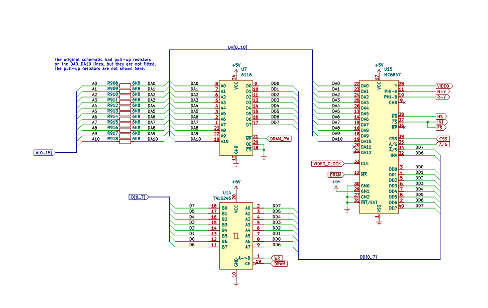
The VDG problem:Last time we talked about how the 6847 expects bus arbitration pulses to clear its address strobes off the bus so the CPU can write to memory. We went over how this creates snow artifacts as the 6847 tri-states the address bus outputs. We also went over how the timing of the specific logic inside the circuit is paramount to making sure the 6847 is off the bus so that the CPU can make an uncontested write operation.
The Schematic:But what if we don’t want to use LS logic from the 1970s to accomplish our video module? Let’s go over the video circuit in detail by looking at the schematic.
![]()
rweather schematic snip linked to github We see that the data bus is separated by a bus transceiver, from the 6847 (VDG – Video Display Generator) and RAM chip data pins. Going over what we know about the VDG from the last time, it has to strobe through all of the addresses on the RAM chip and build a raster 60 times a second no matter what. That's because the 6847 isn’t really a video display processor, it’s a finite state machine (FSM) with selectable states. Some of these states are selected by data pins, and some are selected by separate control signals from an external register typically (in our design they are). The VDG really only knows how to run a few tight loops: scan the RAM and display in text mode, scan the RAM and display in graphics mode and so forth. These “states” in a fixed path tight loop are what makes the VDG a state machine and not truly a dedicated video co-processor. Essentially, it scans the RAM really fast and pushes out a bit stream, as well as create all of the relevant sync and color information pulses over and over; forever, unless you change the state or interrupt them. Think of it as an elevated version of the “TV Typewriter” but with much of that circuit already built into the box, including the character ROM!
The Crux of the Problem:So we have established, essentially, the circuit has to keep the data bus and the address bus clear of contention whenever the 6847 needs to push out a frame to the display. The circuit does this by separating the address bus with a bank of resistors, and the data bus with a bus transceiver. When the /DRAM signal is generated in the chip set the address bus on the VDG cuts out, the data bus aligns with correct directionality, and the RAM chip is selected. Ultimately this creates snow because the CPU does not know when the VDG is on the RAM it only knows it can knock the VDG off the RAM by writing to or reading from it. This works well, it’s simple and cheap but obviously the issues are:
- Timing is tied to the logic family, and the specific construction requiring multiple chips
- Even though the CPU and the VDG are clocked by the same clock, they are not synchronous. The Address decode, write and read cycles of the Z80 prevent the two devices from truly being able to avoid contending with one-another.
- The VDG is knocked off the bus on every single write and read to the display memory, this “second fiddle” bus positioning means lots of artifacts.
- Artifacts are annoying and they can ruin user experience.
- The decode circuits cascade decoder chips, which leads to large ...
-
The curious case of the VZ-200 Chipset (Part 1)
11/26/2025 at 22:25 • 0 commentsIn this Series
We're going to build a replica VZ200, a very interesting off the shelf home computer, done on the cheap, but also quite popular in the markets that it dominated. In this part we will go over the chipset at its heart and try to explain how it's one of the cleverest little minimal designs of its time.
We will work with PCBWay (our sponsor) to build a brand-new backplane system all on cheap 100x100 or smaller PCB's just large enough for the task at hand and were going to do it all up open source, so you can hack on it to your hearts content and maybe make your own!
So come along with me as we explore the chip set of the VZ200, and the cheap computer that took the hearts of many young programmers. It should be a very interesting prospect indeed, and in the end hopefully we get a working computer to show for it.
The Basics
The VZ200 is a Hong Kong based VTECH (then Video Technologies) designed home computer. Produced in 1983 and based around the venerable Z80 CPU, and curiously the 6800 family IC the 6847 VDG (of Tandy CoCo fame). The computer's clock is operating at the NTSC color burst frequency, approximately 3.5795 Mhz. This computer was a first for a lot of kids in the eighties in places like China, Australia and Germany. NTSC versions did exist but the majority of the machines are PAL based (a fantastic story but not why we are here today.)

VZ200 image by way of wiki commons The computer normally outputs in PAL, though NTSC versions do exist. The chrominance and PAL line timings are generated by way of a daughter card, whose schematics have been redrawn by this clever user on GitHub. Video oddities aside, the scope today is simply to go over the 3-chip chip set, because like so many costs reduced computers of the day, it really was able to squeeze a ton of functionality out of such a low chip count.
The Design goals (squeezing blood from stone):
The VZ-200 uses 3 ICs to do all of the address selection and decode, 2 multiplexers (74LS138 and 74LS139) and a Quad OR (74LS32) . It also manages to control the bus arbitration for the VDG, simply as a side effect of fan out. The logic is all standard LS type logic so we can fairly well guess the propagation delay from the data sheets. Since the clock speed of our Z80 is known (approx.. 3.5795Mhz), we can calculate the T≈279.4nS. If we look at the actual logic design we can then simply calculate the timing delays for all of the select lines by doing some simple arithmetic.
We have good schematics for the VZ200, so we don't have to guess how they are all connected. for simplicity of this demonstration I took the liberty of building just the decode section in H. Neemans Digital
![]()
The chip set had to do five things ascertained by simply looking at the outputs:
- Control a number of 2K SRAM chips
- Control a number or 8K ROM chips
- Time High-Z logic for the VDG address lines
- Control a memory mapped IO range
- be cheap.
It is strange on a CPU that has a dedicated IO port instruction would have anything in the way of Memory Mapped IO. IO ports make accessing devices on the bus simple for the CPU but they can also add complexity to the selection logic. It is odd, but also pragmatic.
Z80 Cycles:
Cycle type MREQ RD WR M1 IORQ IN (I/O read) 1 0 1 1 0 OUT (I/O write) 1 1 0 1 0 Interrupt acknowledge 1 0 1 0 0 Opcode fetch (memory) 0 0 1 0 1 Memory reads 0 0 1 1 1 Memory writes 0 1 0 1 1 Bus idle / no cycle 1 1 1 1 1 IO selection on the Z80 happens when the CPU uses the OUT or IN instructions (mostly, but we will only go into that use case here). When this happens, /IORQ goes low, and /RD or /WR goes low as well. There's also another reason /IORQ goes low; that's during an interrupt acknowledge, however in that case M1 goes low. So,...
Read more »


 Lutetium
 esben rossel
 David Davenne
 Robert Hart
 Stefan Wagner
 jareklupinski
 Lasith Ishan
 Joe Burks
 Ahmed Azouz
 John Opsahl