Close
0%
0%

HBSound

DIY Sound Card for A home brew Computer

Similar projects worth following
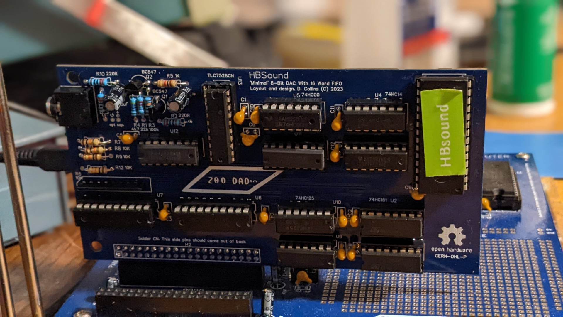
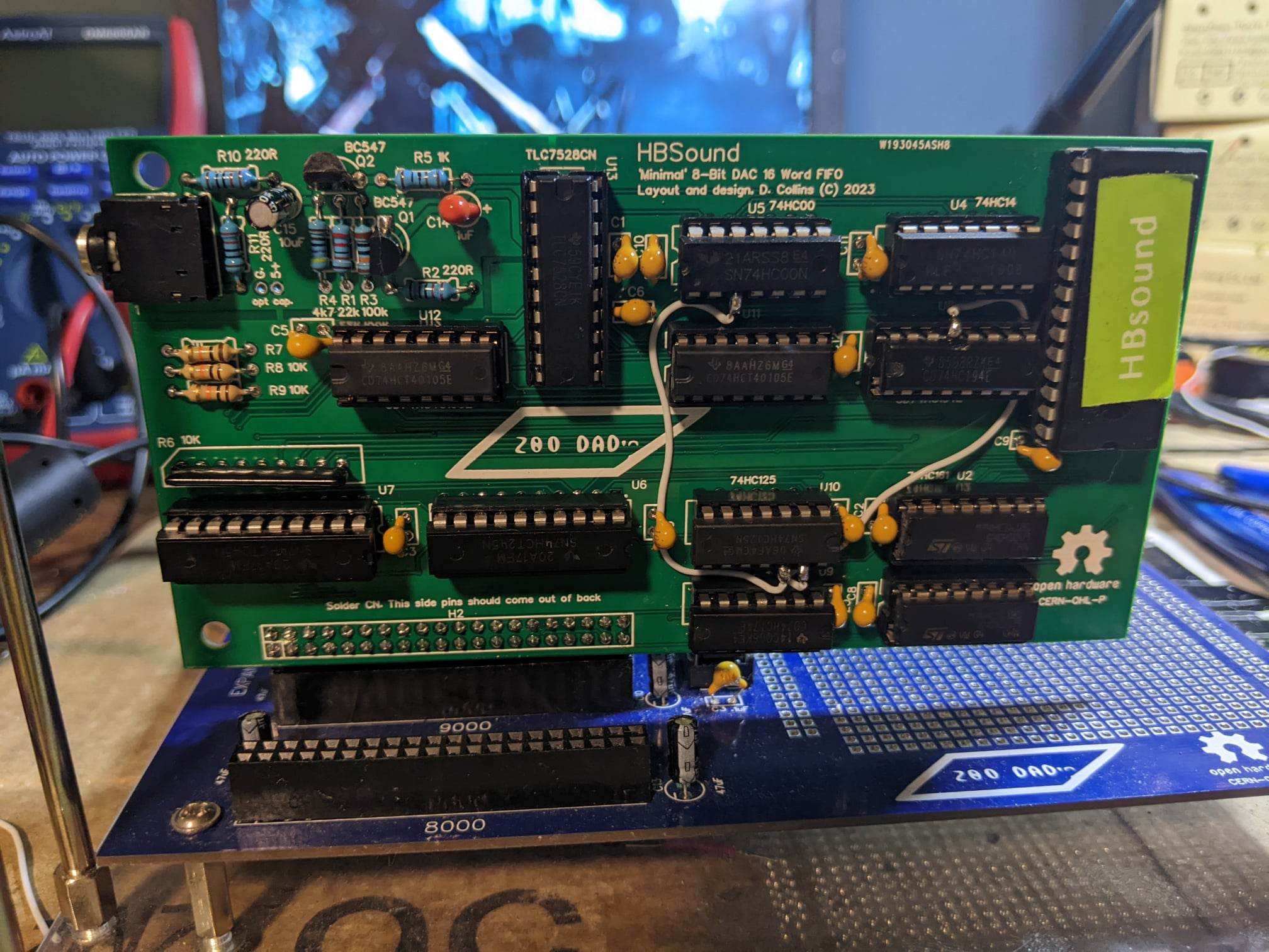
This is a simple design for my 8 bit sound card which features the TLC7528CN 8 Bit Dac and a set of 74HC40105 FIFO Buffers. The purpose of this design is to make a simple sound card that only requires standard Motorola simplified control architecture (such as in the Grant Serle / Jeff Tranter Basic computers). The only required control signals re E, R//W and A0. The FIFO allows for commands to the DAC to be buffered all at once, which gives the programmer more flexibility, and not have to worry about specifically timing the output properly. This design pays homage to the DSS/Covox Sound cards which ran from a parallel port.

This Project is completed:
GitHub for all related information is https://github.com/lindoran/HBSound

HBSound is an attempt to make Hobbyist home brew sound card, based off a simple architecture that can be controlled from even a simple micro controller.


The design goals are:

  1. Based off mostly available parts ( TLC7528 8 bit DAC / 74HCT40105)
  2. Requires only a hand full of minimal Motorola minimal controller signals to operate (E, R//W and A0) 
  3. No DMA, Halting the CPU, wait operation or Interrupts required (but optionally available).
  4. HCT buffered control and data lines to allow for a broad rage of CPU's and controllers.

This is mostly accomplished using the widely available CD74HCT40105 (a CMOS clone of the CD40105 14 word 4 bit FIFO)

The design can be adopted for any home brew computer but the card I will be building is based around the HB6809 Home-brew expansion computer.

First some caveats: 

Every time I do a custom PCB design, I get feedback which I am very grateful for but here's a few things to  keep in mind:

  1. Autodidact warning - I am self taught - this could be 100% wrong - but I did do testing on real hardware to determine its at least effectively working for my use-case.
  2. This is not a high speed design - it does not adhere to high speed design practices, it is meant to work at the maximum E value found in my computer which is 1.8432 MHz.  I should mention Howard W. Johnson / Martin Graham's book on high speed digital design (It is very good if you are in to that sort of thing)
  3. This is a hobby, I do it for fun -  I don't plan to mass produce or sell any of these things that I build and so the build quality is not always going to be what you would expect from a commercially provided, professionally designed product.  Furthermore, I don't expect that I am the best source of information on the "right way to do something" -- you absolutely should take everything here with that grain of salt.

PCBs available on the shared projects store:

PCBWay Shared projects - HBSound


Sponsorship:

PCBWay Sponsored PCB assembly costs on this project during the prototyping phase, if you are interested in their highly recommended fabrication services please check them out.  They offer PCB services, 3d prototyping and metal fabrication as well as PCB assembly services.  Costs are reasonable and the quality even on their prototype boards is very good.  Thank you PCBWay! without contributions like this it would be impossible to move projects along at this speed.


License:

HBSound is open hardware under : CERN-OH-P


 Liability / warranty language from the license

5.1 DISCLAIMER OF WARRANTY -- The Covered Source and any Products are provided 'as is' and any express or implied warranties, including, but not limited to, implied warranties of merchantability, of satisfactory quality, non-infringement of third party rights, and fitness for a particular purpose or use are disclaimed in respect of any Source or Product to the maximum extent permitted by law. The Licensor makes no representation that any Source or Product does not or will not infringe any patent, copyright, trade secret or other proprietary right. The entire risk as to the use, quality, and performance of any Source or Product shall be with You and not the Licensor. This disclaimer of warranty is an essential part of this Licence and a condition for the grant of any rights granted under this Licence.

5.2 EXCLUSION AND LIMITATION OF LIABILITY -- The Licensor shall, to the maximum extent permitted by law, have no liability for direct, indirect, special, incidental, consequential, exemplary, punitive or other damages of any character including, without limitation, procurement of substitute goods or services, loss of use, data or profits, or business interruption, however caused and on any theory of contract, warranty, tort (including negligence), product liability or otherwise, arising in any way in relation to the Covered Source, modified Covered Source and/or the Making or Conveyance of a Product, even if advised...

Read more »

Programmers Document.pdf

This is a short document describing the interface for developers it is (C) 2023 D. Collins

Adobe Portable Document Format - 99.64 kB - 02/20/2023 at 06:16

Preview

Project Files HBSound.zip

here are the back up design files; make changes but please remember this is licensed under CERN-OHW-P which requires attribution and re-licensing under the same.

Zip Archive - 292.28 kB - 02/20/2023 at 06:14

Download

Gerber_HBSound_Final.zip

Final Gerber Files

Zip Archive - 217.21 kB - 02/20/2023 at 06:14

Download

Schematic_HBSound_2023-01-26.pdf

Most recent schematics

Adobe Portable Document Format - 179.27 kB - 01/30/2023 at 04:29

Preview

bottom.png

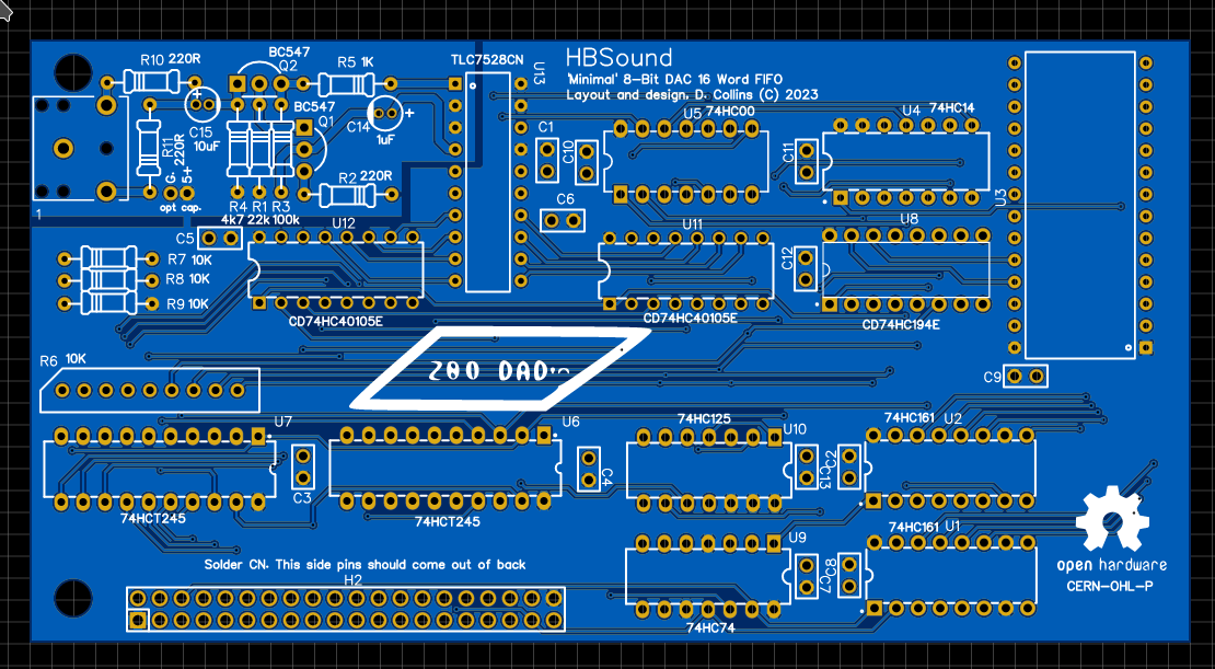
Bottom of the board layout render

Portable Network Graphics (PNG) - 220.83 kB - 01/30/2023 at 04:30

Preview

View all 13 files

  • 1 × W27E257 Memory ICs / EEPROMs
  • 2 × CD74HC161E Logic ICs / Counters
  • 1 × CD74HC194E Logic ICs / Flip-Flops, Latches, Registers
  • 1 × 40 PIN 90 DEGREE 2X20 CONNECTER CONNECTORS
  • 2 × SN74HCT245N Logic ICs / Receivers, Transceivers

View all 23 components

  • LAUNCH! Final Proof Test: Building a Test Sound Player in C

    Dave Collins02/17/2023 at 20:00 0 comments

    Introduction:

     So over the last week or so, I have been building on trying to test out HBSound at speed in a way that verifies all of the different subsystems of the module.  In order to do that I had to make some slight modifications to the system rom on  the HB6809.   This was quite the learning curve and along the way I managed to pick up "Learn Multiplatform Assembly Vol 2" which covers the 6809 (as well as RISC V, the PDP-11 and a handful of other CPUs.).  I Highly recommend this book!  

     Along the way I settled on writing the test program in C, because my assembly fluency is still an ongoing process.   This was a relative success, and I managed to get a functional test program that streams the audio frame data to the card over the bus, and also simultaneously updates the terminal with output.  Its actually quite a good demonstration of the capabilities of the interface, that even with a higher level un-optimized language can produce working output without the use of any direct assembly language programing.

    Proof PCBs for Final Testing:

    So almost as soon as I finished building the prototypes, and determining the fixes our sponsor PCBWay stepped up and offered to re-make and ship new proofs to test the design changes.  I also ordered a small PCB to start working on the ROM / RAM expansion which I was able to build test and verify, everything was working very well (more on that later).   

     The PCB's came in about a week, to my door everything was perfect! I did have some issues with DHL, but this can hardly be blamed on PCBWay.  I submitted both orders, they set up production and delivered both in the same box, despite both projects having completely different build times.  I was very impressed that I didn't have to wait for a second box.

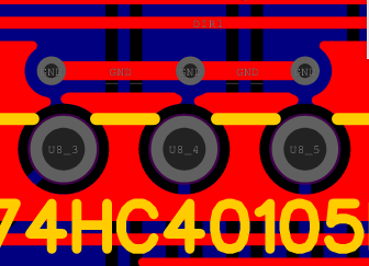
     The HBSound Proofs were ordered in this lovely blue solder mask, I wanted them to match the main system PCB's final build color so It was good to see that when you request a mask color change (for most, but not all)  there wasn't an extra charge.    Additionally I had done quite a bit of work adding "Stitching" vias to the revised design.  This is a technique I picked up from watching the Byte Attic ( aka Bernardo Kastrup).  This is a way of joining copper fields with a trace and two vias to transfer connection between two isolated areas of the board. This allowed for no larger areas of the copper fill to be missed by the EDA software, and provides for a cleaner return path to ground for all devices. Even though this is not a high speed design, we are mixing analog and digital ground planes without a multi-layer board, and so I wanted the coverage to be as consistent as possible.

     The Added stitching vias to the design did not change the price, and even with the close drill distance and detailed work involved in getting these tiny additions the actual PCBs were spot on and perfect, there were no shorts or issues even with the close clearance in some areas.  Especially next to the bus connector:

      Or this section here next to one of the FIFO chips:

    Over all I was quite pleased with the boards that I had made and I am continued to be blown away by the access to these kinds of prototyping services.

    A Pathetic way to play songs PathiTrack6809:

    I wrote a test program in C It is a simple tracker program that builds 15 byte sample frames from a per-calculated list of timing count data, sends them to the card when the buffer is empty (until it shows full).  Essentially the loop is simple:

    • Check to see if buffer is empty if so
      • send frame data until its full  unless it is not then
    • do other stuff while waiting,
      • periodically checking if the buffer is empty
      • update tracker display
    • repeat

    A document describing the interface for developers can be found in the GitHub for this...

    Read more »

  • Prototype Assmbly, issues and board review.

    Dave Collins01/28/2023 at 19:23 0 comments

    IT WORKS!!

    Board review

    So after receiving the boards back from the sponsor PCBWay, which took about a week.  I was very pleased with the build quality, which continues to exceed my standards for what a prototype board should look like.  I have no doubt in saying, that these boards hold up even with the lowest cost build options.  In fact when mounting the edge connector on the board I made a mistake and had to manually remove the connector to solder a new one, and was concerned because usually there is some damage to the solder masking around the rework area on prototypes with manual de-soldering.  But to my surprise, there was only mild wear on the masking which needed to be cleaned up by applying some nail varnish (but not much) before re-populating the connector in the board.  This is a huge plus if you are working on a prototype and find the need to de-solder a large part but do not have a fancy de-soldering pump. Other services use much less consistency in the amount and quality of mask that is applied.  This time I did the bog standard green which is  what comes with the low cost option on many other services and I am pleased to say even on economy masking, the level of quality is really there, this may be due to multiple coats or just a slower application; whatever the case I was very happy with the results.

    Full disclosure disclaimer: PCBWay is sponsoring the prototyping by providing them for free.  I received no money to make these statements, and my observations are my own.  Additionally PCBWay has not requested to review or change any of my statements prior to making them.


    HB6809 In the news, the HBSound and more:


    About a week ago I did a YouTube video reviewing the design of the control unit on my sound card, This was kind of a follow up to the last journal entry. I also did some block diagrams in my lab notebook. I also updated everything in the files section with the newest schematic, high resolution PCB rendering files as well as a excel spread sheet breaking out the math for the counts in the state machine .HEX (which is also included).  I'd like to test the new gerbers out by having them made to make sure that they are working which may be a week or two out.  I don't anticipate any of the issue with the design updates (however silly mistakes can happen).

    Another thing of note: a small clone of the Jeff Tranter / Grant Searle (and i guess now me, Lol) 6809 design was made by hardware hacker antibyte!  This thing is a tiny 6809 single board computer (with a very useful expansion port).  The parts were sourced to be what is generally available from PCB assemblers IE, you should be able to just order one and have it assembled (with acceptation of the through hole parts that is!)  The design uses one of the expansion spaces in my design to expand the rom space; I very much love this idea!   I think I will build a RAM / ROM expansion for my computer based off of this.  The clock circut and powering is different (he integrates a USB to serial chip, as well as other useful bits (a baud-rate generator).  I also had planned to re-work the clock oscillator on the computer to make use of faster 63c09 chips -- this might require a redesign of the motherboard -- more on that later!

    Issues with the CD 74HC40105 datasheet:

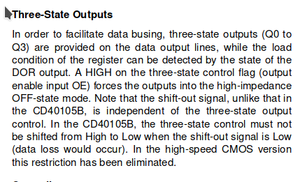
    I had encountered issues with the modern 10405 FIFO equivalents from TI mainly with the /OE operation and specifically how it was documented in the datasheet.

    In the CD74HC40105 datasheet the /OE pin is documented this way:

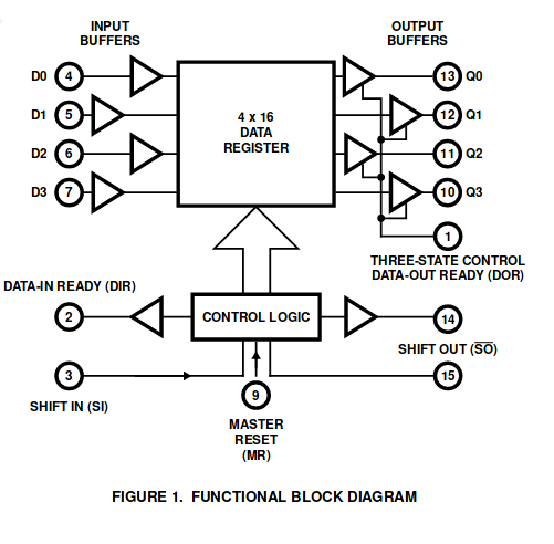
    with the following block diagram:

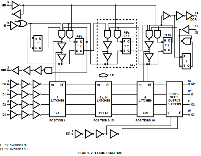
    see what is missing here - no mention is made of the OE line at all.  To add insult to injury, this is the logic diagram:

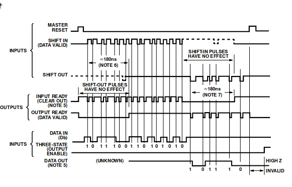
    This seems to suggest the /OE line only affects the Q0 - Q3 outputs.  Even the master timing diagram doesn't seem to show any thing different:

     
    However upon building up the...

    Read more »

  • Prototype, ready for manufacture

    Dave Collins01/06/2023 at 17:03 0 comments

    PCB Design is complete!  wow that took a while.

    I thought I'd sit down and talk about the HBSound for a bit. If you don't know, HBSound is the DAC based sound card i've been developing for some months for my home brew computer, the HB6809.  I haven't updated the Hackaday.IO site for a while and the reasons for this are varied but basically I am ready to share what I have for a few short falls at the end.  I had a computer crash and had to re-establish a tool chain completely on my laptop.  Its a better set up and I purchased a New old stock docking station to be able to un-dock my laptop and take it with me to work so I can update the project files on my lunch breaks.    I didn't loose any important project files, most of this was in the cloud, but re-establishing a firm working set up was time consuming.  I was planing on doing a video walk through of the control unit but as I've come down with a case of strep writing out my thoughts here may have to be good enough for a while.

    First some caveats: 

    Every time I do a custom PCB design, I get feedback which I am very grateful for but here's a few things to  keep in mind:

    1. Autodidact warning - I am self taught - this could be 100% wrong - but I did do testing on real hardware to determine its at least effectively working for my use-case.
    2. This is not a high speed design - it does not adhere to high speed design practices, it is meant to work at the maximum E value found in my computer which is 1.8432 MHz.  I should mention Howard W. Johnson / Martin Graham's book on high speed digital design (It is very good if you are in to that sort of thing)
    3. This is a hobby, I do it for fun -  I don't plan to mass produce or sell any of these things that I build and so the build quality is not always going to be what you would expect from a commercially provided, professionally designed product.  Furthermore, I don't expect that I am the best source of information on the "right way to do something" -- you absolutely should take everything here with that grain of salt.

    all of that in mind, I do from time to time take 'service in kind' sponsorships, every benefit I get from that is directly fed back into my projects and I greatly appreciate that support, as I don't think I would be able to do much of any of this with out it.

    That out of the way here we go:

    The control bit:

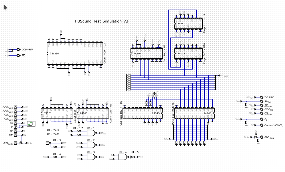
    I spent a ton of time working on the control portion of the sound card.  Several iterations of this design were assembled in H. Neemans DigitalI wound up going with this simplified design.  I wanted to try to stick to discrete components that are mostly available still from digikey / Mouser -  I could have most likely built the counter logic within a single or maybe to GAL's but for working with the parts I had on hand, and what I know I went with a Winbond W27E257 EEPROM as my only used / new old stock part.  I had to use a 28c256 in the simulation but the actual part was the 12v eeprom.  You can still get these in mass as pulls from 486 era PC motherboards on Amazon / Ebay and I have a ton -- I suspect many will also.  The Fifo Selected is a standard CD74HC40105E, this allows the bit stream to be built in a buffer, which can give the programmer more time to do things while the slower DAC clock is shifting out the data.  This technique was used in the famous (infamous? ) Disney Sound Source.   Though, in that case a 555 timer was used to shift out the data at around 7kHz.  The inevitable problem with this previous  design is that the clock was inconsistent due to using a RC / 555 driven count (which would change the pitch off of a baseline), and many have argued that the similar COVOX sound adapter was a better solution as considerable better bit rates could be achieved even using a 8088 to control the timing.

    Essentially the control piece does four things. First, it allows a set of flags...

    Read more »

  • Simulations

    Dave Collins12/02/2022 at 12:25 0 comments

    This week got crazy busy, still working on the sound card and I've mostly finished the simulations.  some of them have a HC line to halt the main DAC clock. this was omitted in the final design for simplicity sake.  take a look they are all built using "Digital" and uploaded into the files section.

    "Digital" is a Logisim digital logic simulator by H. Neemann - though it is relatively hard to google the git hub due to the name. Fortunately, a conveniently provided link is above. 

  • Prototype 1 issues, a second case study in optimizing failing process.

    Dave Collins11/07/2022 at 03:38 0 comments

    Status:

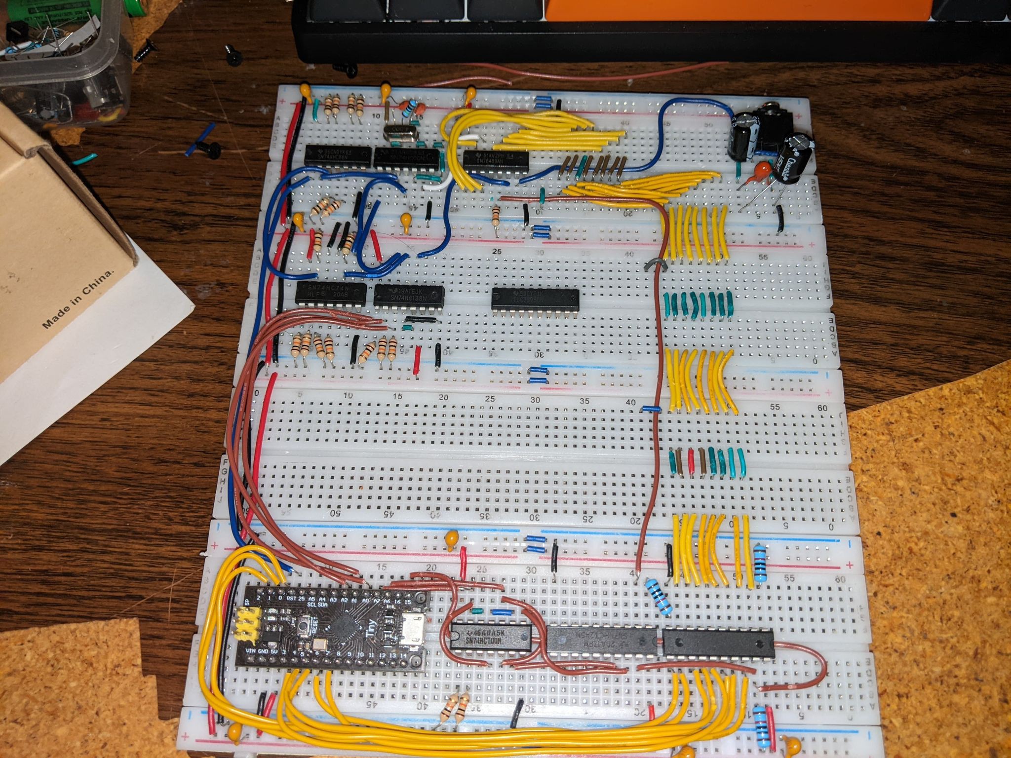
    HBSound development continues, Many have seen this picture kicking around social media. This is what I'm now calling prototype 1.  And some of the things I learned from this build are its complexity is it's downfall.  When I built the top module I felt it was reasonably successful jumping point because it actually worked.  This led me to add in more complexity and, I believe that where the issues started.  Prototype 1 used a large NAND to combine all of the output signals, and the ready signals (plus some select able buffered clocks) to make the shift out clock.  For a lot of reasons this was a bad Idea.  in fact the design was so busy, and chaotic I am hesitant to share it further than the block diagram because, I am afraid in doing so I open up opportunity to optimize a thing which probably is so flawed it should not exist.  That being said,  in prototype 2 I have to go so much simpler.   The first issue is the SN76489, its a wonderful part for its time, but it has some issues which require layers of complexity to over come.  Firstly it requires a 3.5-4 MHz clock to create compatibility with period correct machines, most of the source music is written with this timing range in mind and so its a requirement if you want to play music files from other machines that also have this sound chip.  The part also has to be silenced from the host machine using initialization. Until then it comes up in a random state and makes noise out of the output.   To over come this typically a SR flip flop is used to gate the PSG's clock, this requires more control logic and additional logic to XOR the system reset line which again adds more complexity. This set up allows you to halt the PSG clock but this does not completely reduce the noise from the PSG.  The other issue was trying to use the FIFO in a pseudo write - through mode this failed.  The timing window was too small, too many signals had to settle in the gate, this created among other things, unreliable timing.    

    So where does that leave us?


    I think I need to take a look at picking one chip for the card and I'm leaning widely towards the DAC.  A DAC provides the ability to create very robust sounding output, with digitally generated tracking using spare cycles between operations; there's a large body of sample work as the design I'm shooting for is very compatible with the COVOX / DSS for the PC only with a beefed up oscillator design.   Another big benefit is the part is still available on Mouser / DigiKey.   The PSG has complications which make it harder to use reliably, requires gated clock generation, that has to be halted to really effectively use it as a select able module,  the part also has to be pragmatically silenced in order to really shut down the sound generation completely.  Another issue which is a small problem since they are still plentiful  the PSG is new old stock.  

    I think the choice is clear, I should use a single chip DAC and stop messing around with trying to provide a optional write through mode.  The 2-32 kHz sample rate (which is software select-able) I'm shooting for is more than enough to produce far better sound quality than even the reference Disney sound source, which had a fixed 7-8Khz sample rate provided through a 555 timer.  My design uses a fixed crystal oscillator to produce the base clock and a counter chip to produce the pulses. 


    I decided this time to build up the control logic in "Digital" logic simulator.  Its a nice Logisim clone, that's actually got properly functioning 74254 bus transceivers, which i used HCT variety in my build so I could use faster HC logic and still interface a TTL CPU.   You will recognize the Motorola specific architecture signals are used here but the basic design should be able to be adapted to any basic single clock...

    Read more »

  • The plan so far.

    Dave Collins10/26/2022 at 03:29 0 comments

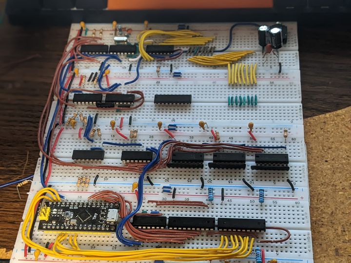
    So for starts I am building a rough bread board prototype, which i can control with a easy to program attiny88 dev board ( I use a cheep USB programmer as the usb ports on these are practically worthless.)  I can run a simple test program at the moment that sets the registers in the PSG (using the control logic on the bottom board (all HCT).  Next is to hook up the FIFO module, and get it to do write through:

    • Write through will pass along the current data to the PSG / DAC immediately following the rising edge of /WRITE signal from the control logic.
    • The buffer will hold the data only if the PSG or DAC are not ready to receive the data (which at normal speeds wont likely be more than a clock cycle.)

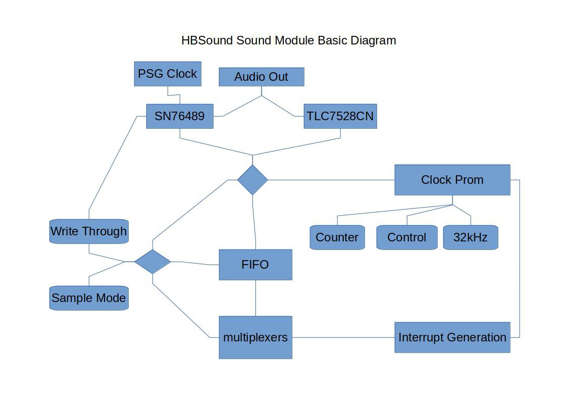
    After that is working, I will start work on a design to implement an adjustable clock, with interrupt generation as an option that can be used to set a sample rate based on a maximum of 32 kHz.  The basic diagram for the card is as follows:

    The design is still fluid, but I am hoping once I get the kinks worked out of write through I should be able to proceed on to getting the TCM (Timer / Clock Module) finished.

View all 6 project logs

Enjoy this project?

Share

Discussions

Similar Projects

Does this project spark your interest?

Become a member to follow this project and never miss any updates