Dave Collins
-
LAUNCH! Final Proof Test: Building a Test Sound Player in C
02/17/2023 at 20:00 • 0 commentsIntroduction:
![]()
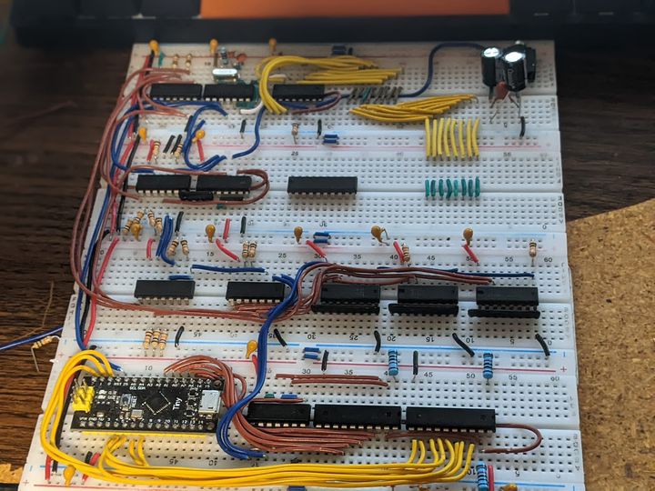
So over the last week or so, I have been building on trying to test out HBSound at speed in a way that verifies all of the different subsystems of the module. In order to do that I had to make some slight modifications to the system rom on the HB6809. This was quite the learning curve and along the way I managed to pick up "Learn Multiplatform Assembly Vol 2" which covers the 6809 (as well as RISC V, the PDP-11 and a handful of other CPUs.). I Highly recommend this book!
Along the way I settled on writing the test program in C, because my assembly fluency is still an ongoing process. This was a relative success, and I managed to get a functional test program that streams the audio frame data to the card over the bus, and also simultaneously updates the terminal with output. Its actually quite a good demonstration of the capabilities of the interface, that even with a higher level un-optimized language can produce working output without the use of any direct assembly language programing.
Proof PCBs for Final Testing:
So almost as soon as I finished building the prototypes, and determining the fixes our sponsor PCBWay stepped up and offered to re-make and ship new proofs to test the design changes. I also ordered a small PCB to start working on the ROM / RAM expansion which I was able to build test and verify, everything was working very well (more on that later).
The PCB's came in about a week, to my door everything was perfect! I did have some issues with DHL, but this can hardly be blamed on PCBWay. I submitted both orders, they set up production and delivered both in the same box, despite both projects having completely different build times. I was very impressed that I didn't have to wait for a second box.
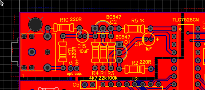
The HBSound Proofs were ordered in this lovely blue solder mask, I wanted them to match the main system PCB's final build color so It was good to see that when you request a mask color change (for most, but not all) there wasn't an extra charge. Additionally I had done quite a bit of work adding "Stitching" vias to the revised design. This is a technique I picked up from watching the Byte Attic ( aka Bernardo Kastrup). This is a way of joining copper fields with a trace and two vias to transfer connection between two isolated areas of the board. This allowed for no larger areas of the copper fill to be missed by the EDA software, and provides for a cleaner return path to ground for all devices. Even though this is not a high speed design, we are mixing analog and digital ground planes without a multi-layer board, and so I wanted the coverage to be as consistent as possible.
The Added stitching vias to the design did not change the price, and even with the close drill distance and detailed work involved in getting these tiny additions the actual PCBs were spot on and perfect, there were no shorts or issues even with the close clearance in some areas. Especially next to the bus connector:
![]()
Or this section here next to one of the FIFO chips:
![]()
Over all I was quite pleased with the boards that I had made and I am continued to be blown away by the access to these kinds of prototyping services.
A Pathetic way to play songs PathiTrack6809:
I wrote a test program in C It is a simple tracker program that builds 15 byte sample frames from a per-calculated list of timing count data, sends them to the card when the buffer is empty (until it shows full). Essentially the loop is simple:
- Check to see if buffer is empty if so
- send frame data until its full unless it is not then
- do other stuff while waiting,
- periodically checking if the buffer is empty
- update tracker display
- repeat
A document describing the interface for developers can be found in the GitHub for this project it is located at: https://github.com/lindoran/HBSound/tree/main/Documentation
Additionally there is some code for calling the character output routines, which are built into the machine language monitor ASSIST09. This was explained in a post over at the HB6809 Hackaday.io project page.
Since the computer only currently has 32kb of RAM storing unsigned raw 8 bit samples gets very spendy as far as how many ms of playback you can actually fit (just a few seconds). RLE would help a bit, but it would depend on how many bytes actually repeat in the sequence. You could go further by interrelation and soft augmenting the bit depth by limiting the actual levels to 6 or 5 bit resolution but this would reduce quality but would almost definitely produce more sequential data. The actual decoding algorithm would have to be written in assembly language to be fast enough in order to not under run the buffer. I suspect this kind of coding was used in systems that produced digital audio using non-conventional means like in the Super Nintendo Tales of Phantaisia, or Ghost Busters for the C64.
The first unique subroutine is simply to fill the buffer. We use pointers to define the location in memory of the device, and these are set by a '#DEFINE' statement at the top of the source. Essentially, what this does is to peek at the flags on the HBSound until it sees the value 2. This indicates the buffer is full, if it sees a zero set in the frequency count variable it skips over the square wave generation loop, which skips the note completely (sends no transition data.) The If statement, checks to see if the count is reached and if it has been then it inverts the frequencyState variable which sets up a 50 % duty cycle at the output of the dac until a counter defining the delay expires, then a new note is sent.
void fillBuffer (unsigned char maxFrequencyCount) {
    while (*flags != 2) {       // while not full
        if (maxFrequencyCount == 0)  {           // handles control code
            frequencyState = 0;
            goto CNTCODE;
        }

        frequencyCount++;

        if (frequencyCount == maxFrequencyCount) {
            frequencyState = !frequencyState;   //switch dac between high and low
            frequencyCount = 0;
        }
        CNTCODE:
        *sample = frequencyState;
    }
}
The main subroutine manages sending the data to the screen and calls the fillBuffer subroutine, It builds the screen using printf statements, and then in between frames updates the screen using a combination of printf statements and ANSI / VT100 Control codes, since the terminal has its own screen buffer and control code processing we can sort of "cheat" some of the functionality of the results.
int main() {
    // console redirect for CMOC
    setConsoleOutHook(newOutputRoutine);

    // clear the screen and set up the on screen graphics
    printf("%c[2J",27);
    printf("---------------+\n");
    printf("               |\n");
    printf("               |\n");
    printf("               |\n");
    printf("               |\n");
    printf("               |\n");
    printf("               |\n");
    printf("               |\n");
    printf("               |\n");
    printf("               |\n");
    printf("---------------+\n");
    printf("Frame Note Tone\n\n");
    printf("PathiTrack6809 (C) - 2023 D.Collins\n\n");
    printf("Mario Bros ""Ground Theme"" \n");
    printf("Original Arr. Koji Kondo,1985");

    printf("%c[H",27);

    *control = 3;  //Set DAC Clock to slowest speed
    unsigned int tones = sizeof(noteslist);
    unsigned int note;
    for (note = 0; note < tones ; note++) {  // determines what note we are on
        scpos++;
        if (scpos == 9) {                    //this manages the tracker window
            printf("%c[H",27);
            scpos = 0;
        }
        // right before the note plays...
        printf("\n    : %3d | %2d",note,noteslist[note]);  // prints curent note
        // this is one note
        while (bufferPeriod != BPM) {
            while (*flags !=1) {        //while not empty
              // do stuff here
            }
            bufferPeriod++;
            fillBuffer(noteslist[note]);
            // or do stuff here!
            printf("%c%d",13,bufferPeriod);        // prints the position in frame
        }
    frequencyCount = 0;    // counter for frequency
    frequencyState = 0;    // state of frequency
    bufferPeriod = 0;
    }
    scpos = 0;
    *control = 0;
    printf("%c[18;0H",27);
    softStart();            //Return to monitor
    return(0);
}
The amount of time between frames is approximately 2mS -- this is an eternity for a CPU running at almost 2 MHz. Since much of those cycles are taken up by the relatively robust printf statement (it ads a large chunk of assembly code to the end result) we have to be kind of thrifty with what we do. I probably could have used control codes to do a scrolling note pan, like most trackers have but instead I settled for overwriting from the top down, and using the carriage return to move the cursor back to the beginning of the first field of the tracker data. I did use tabulated formatting in the printf statement which is the lions share of the code from the standard lib. If this program were written in assembly it would most definitely be considerably smaller and we might even be able to pull of a little visualizer in ASCII, or forgo those completely and do a much faster data rate
Gerber availability:
As of today the Gerber files are uploaded to the repository at:
https://github.com/lindoran/HBSound
I consider this project in more or less a finished state, its been a long arduous journey but I think I learned a ton during this project and I am excited to translate that to the next one.
Final design reflections:
Over all I am very happy with the results here, but no design is perfect, and I do have some reflections on what could be done better or changed here to make things work a bit nicer. Over all the EEPROM worked good as a clock divider, it is however kind of a waist of space on the board and I believe the whole design could have been under the cheaper 100x100 size spec if I had opted for some kind of custom logic or a programmable controller. The use of a ATTTiny chip here (as there are only 2 control lines) would have been the most likely choice, the only issue being in that case the clock synchronization would have to be completely done over again. Even a GAL has a smaller footprint and well within the limits of generation of a single low facing pulse based on 4 addresses; I may have even been able to work in the clock synchronization as well.
The TLC7528CN has a active low !WR line, and while the datasheet calls out this is to latch the data into the DAC; I had found through testing that what the datasheet calls a latch is more or less this is a sample and hold. This meant that I could leave the inputs wide open by placing the !WR low all the time. This makes the discrete part behave more like a resistor dac. The only issue with this is it generates a few spurious noise like artifacts as the outputs of the flexible latch settle. In the original DSS design which uses a simple ladder dac you see these same artifacts, as there is no way to stop the analog design from seeing every transition. These could be eliminated completely by using the DOR line from the flexible latches (or simply inverting the output of the or gate). Since this simplified the design and it had worked more or less in testing I didn't really feel the need to disable the DAC inputs especially since the frequency they change at is incredibly slow (a few kHz). Lastly the DAC itself is a two channel dac, it would technically be possible to duplicate everything on the board and create a two channel output, adding two of everything would mean more chips / logic and a significantly more expensive card.
What's next:
So next I'd like to switch gears and look at the over all design. I'd like to work on a memory / ram rom expansion and I've thought about doing a 128k ram / 40k rom expansion. Additionally threes some work that could be done eliminating the recursion in the combo rom. Essentially there are 2 sets of serial control subroutines, when really all we need is 1 set. Since the design I am looking at would use system calls from ASSIST09 to control the screen and input, I would need to go over extended basic and eliminate the recursion. I would like to change the decoding circuitry and perhaps design a custom GAL that does all of the address selection. Have a number of projects centered around restoring a ZX81. But for now the plan is to take a few days off, as I have been working fairly consistently since about a week ago to get everything finished for a weekend release :)
If anybody has any questions please feel free to leave a note, and thanks for taking the time to read about my mad projects!
- Check to see if buffer is empty if so
-
Prototype Assmbly, issues and board review.
01/28/2023 at 19:23 • 0 comments![]()
IT WORKS!!
Board review
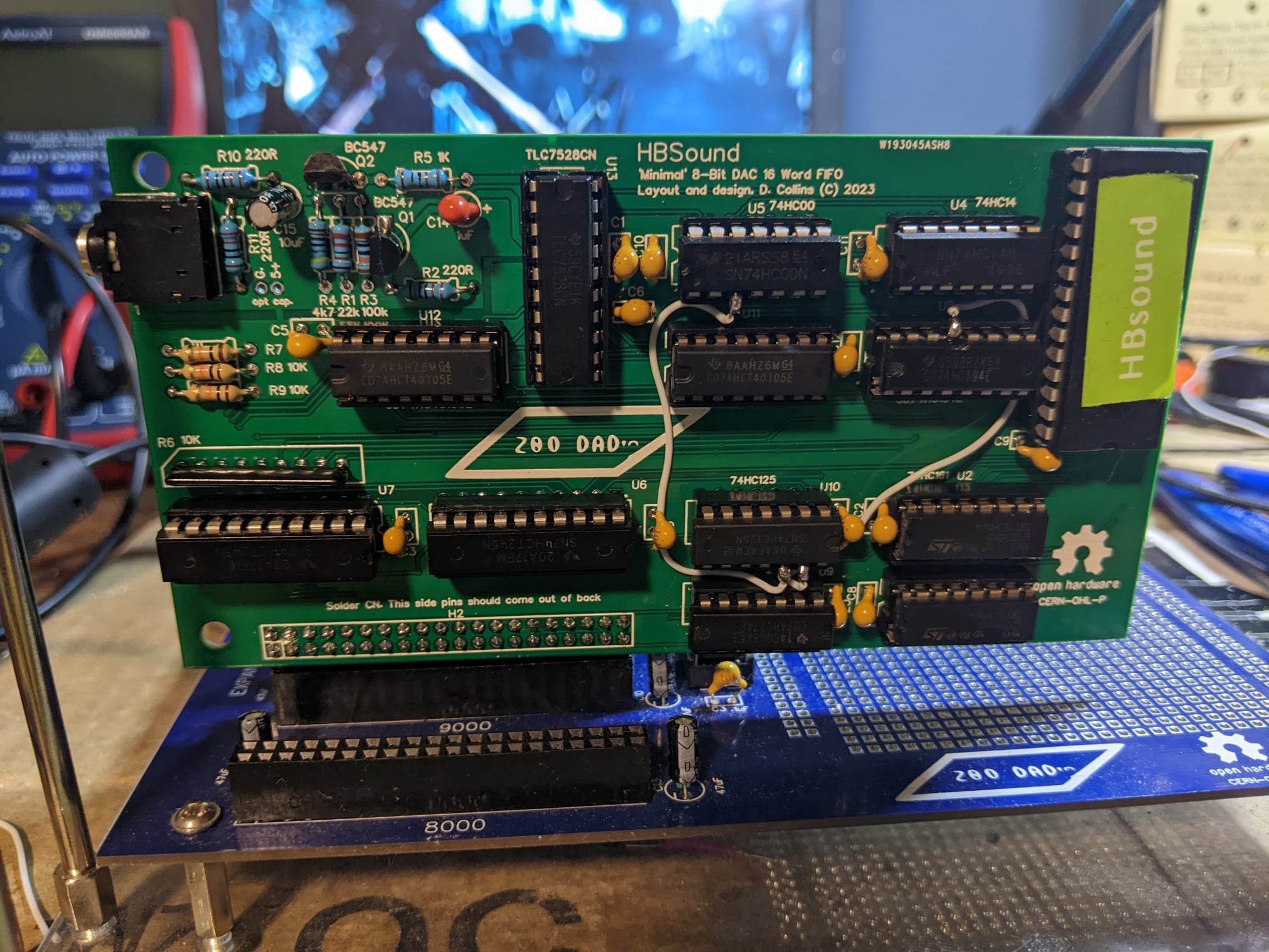
So after receiving the boards back from the sponsor PCBWay, which took about a week. I was very pleased with the build quality, which continues to exceed my standards for what a prototype board should look like. I have no doubt in saying, that these boards hold up even with the lowest cost build options. In fact when mounting the edge connector on the board I made a mistake and had to manually remove the connector to solder a new one, and was concerned because usually there is some damage to the solder masking around the rework area on prototypes with manual de-soldering. But to my surprise, there was only mild wear on the masking which needed to be cleaned up by applying some nail varnish (but not much) before re-populating the connector in the board. This is a huge plus if you are working on a prototype and find the need to de-solder a large part but do not have a fancy de-soldering pump. Other services use much less consistency in the amount and quality of mask that is applied. This time I did the bog standard green which is what comes with the low cost option on many other services and I am pleased to say even on economy masking, the level of quality is really there, this may be due to multiple coats or just a slower application; whatever the case I was very happy with the results.
Full disclosure disclaimer: PCBWay is sponsoring the prototyping by providing them for free. I received no money to make these statements, and my observations are my own. Additionally PCBWay has not requested to review or change any of my statements prior to making them.
HB6809 In the news, the HBSound and more:
About a week ago I did a YouTube video reviewing the design of the control unit on my sound card, This was kind of a follow up to the last journal entry. I also did some block diagrams in my lab notebook. I also updated everything in the files section with the newest schematic, high resolution PCB rendering files as well as a excel spread sheet breaking out the math for the counts in the state machine .HEX (which is also included). I'd like to test the new gerbers out by having them made to make sure that they are working which may be a week or two out. I don't anticipate any of the issue with the design updates (however silly mistakes can happen).
Another thing of note: a small clone of the Jeff Tranter / Grant Searle (and i guess now me, Lol) 6809 design was made by hardware hacker antibyte! This thing is a tiny 6809 single board computer (with a very useful expansion port). The parts were sourced to be what is generally available from PCB assemblers IE, you should be able to just order one and have it assembled (with acceptation of the through hole parts that is!) The design uses one of the expansion spaces in my design to expand the rom space; I very much love this idea! I think I will build a RAM / ROM expansion for my computer based off of this. The clock circut and powering is different (he integrates a USB to serial chip, as well as other useful bits (a baud-rate generator). I also had planned to re-work the clock oscillator on the computer to make use of faster 63c09 chips -- this might require a redesign of the motherboard -- more on that later!
Issues with the CD 74HC40105 datasheet:
I had encountered issues with the modern 10405 FIFO equivalents from TI mainly with the /OE operation and specifically how it was documented in the datasheet.
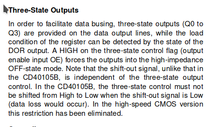
In the CD74HC40105 datasheet the /OE pin is documented this way:
![]()
with the following block diagram:
![]()
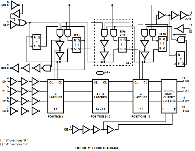
see what is missing here - no mention is made of the OE line at all. To add insult to injury, this is the logic diagram:
![]()
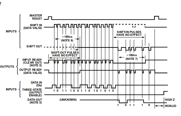
This seems to suggest the /OE line only affects the Q0 - Q3 outputs. Even the master timing diagram doesn't seem to show any thing different:
![]()
However upon building up the prototype, I discovered that the flags from the FIFO's were not updating while the /OE pin was set high. This is a issue i never tested for on the breadboard when I was working with the part during the design phase, as the datasheet seemed to indicate that those outputs would always be representative of the status of the register.Imagine my surprise, when low and behold I was having issues with this specific thing. I suspect this has to do with the changes to prevent data corruption, but unless somebody de-caps a CD74HCT40105 and looks at the logic, we will have to wonder.
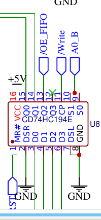
This causes a issue with my design:
![]()
I run the /OE signal directly from the control register, so when the register is set to stop the outputs on the FIFO they lock in a state which makes them unusable for the current flags register on my sound card.
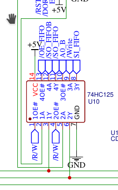
To resolve the issue I re-purposed a tri-state buffer from the design which was terminated to +5V:
![]()
Now the signal from the shift out clock (which I re-named SO_FIFOB) is gated by the /OE_FIFO signal. I also tied the output of the buffer to +5v through a 10k resistor in order to prevent the clock state from floating when it is disabled. Additionally I tied the output enable line to ground on the FIFO's to lock the outputs to always on.
![]()
![]()
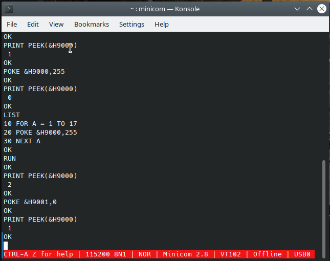
After making the changes, I tested with a few pokes in basic and everything is performing as planned.
![]()
It doesn't look like a lot but this is actually a complete proof of function. Sending a poke to location 9001 (off screen) a value of 7, we send a 111 to the control register. This disables the DAC Clock and sets the clock to 7.2kHZ. Peeking at the address space of slot 9000 we see the register returns a 1, this means that the FIFO is showing that it is empty and has no more data to output. DOR is LOW, DIR is HIGH but they are inverted by the NAND gates so the returned value is 1. If we send 1 byte to the FIFO with another poke to 9000, and then peek at the address again we see a 0. This means the DIR / DOR are both HIGH, but are inverted and so the return value is 0. If we run the short program to send a bunch of bytes to the address we flood the FIFO and it overflows. Since it is full if we peek at the address we see that it is returning 2, this means that DOR is HIGH, and DIR is LOW as the signals are inverted by the NAND gate. If we again poke 9001 and set the control register to 0, this turns the DAC CLOCK back on and sets the CLOCK to its fastest speed of 32kHz. Peeking at the address again we can see the FIFO is emptied, and the flags are reading 1 again.
Scope analysis:
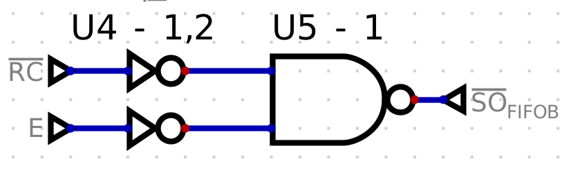
Taking a look at the NAND gate that is the output of the OR function:
![]()
We can see this takes the output of the state machine and does a OR operation on it and the system clock 'E', so that when both signals go LOW the /SO_FIFOB signal is LOW. This is exactly what we want as this grantees the shift out happens only on the falling edge of the system clock (If you would like this is further explained in the last entry in this space).
If we probe this output with an oscilloscope, and run some basic pokes:
![]()
We can see that the scope shows the clock changing frequency:

Probe point 
32kHz 
16kHz 
8kHz 
7.2kHz 
Edges of clock/Period I also did a test of the edges of the clock which show significant ringing, some of this is due to the poor ground point for the probe but also could be an impedance mismatch on the trace and bodge from the output of the gate. The ringing is not anything I think I need to be concerned about as the speed of the edges are slow enough this is likely not to matter, additionally the amplitude is not above (or below) the switching threshold of the input. If I have issues at speed I can simply install a termination resistor in line with the output (or input).
Whats next?
I need to work on a test program that loads data at speed, as Microsoft Enhanced Basic is not fast enough to update the FIFO to produce anything more than a small 200Hz square wave (which ill save your ears from). I will definitely do something in assembly to demonstrate the card by playing a digital sample. I want to as stated before order some replacement PCB's after knocking together a quick memory expansion (possibly in the prototype area). It is Ideal for this as it is going to be near all the signals I will need. I'll be switching to a larger, electrically erasable EEPROM and a larger RAM chip. Additionally I have a ZX81 I am restoring that takes up some of my time as well, you can follow along with the progress on my 'hack a day pages' blog here. I am also working on a new integrated terminal board in my notebook, which I'm not quite ready to share all of but suffice to say I am looking at a few modern QPLD socket-able serial chips from maximum integrated. Over the next week or so the focus will be on getting an assembly tool-chain set up and writing code for the sound card, so watch this space for updates. Thanks for taking the time to read about my little projects, and thanks again to PCB way without their support projects like this would take considerably longer. If you have any questions feel free to drop me a line I will try my best to answer.
-
Prototype, ready for manufacture
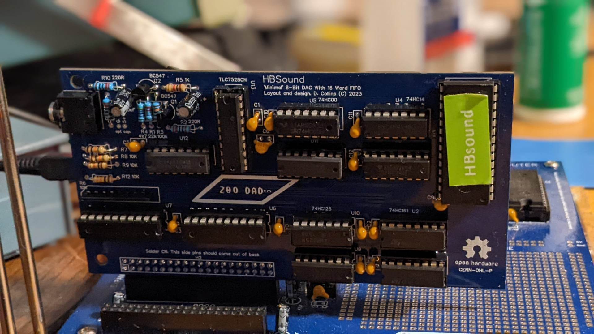
01/06/2023 at 17:03 • 0 commentsPCB Design is complete! wow that took a while.
![]()
I thought I'd sit down and talk about the HBSound for a bit. If you don't know, HBSound is the DAC based sound card i've been developing for some months for my home brew computer, the HB6809. I haven't updated the Hackaday.IO site for a while and the reasons for this are varied but basically I am ready to share what I have for a few short falls at the end. I had a computer crash and had to re-establish a tool chain completely on my laptop. Its a better set up and I purchased a New old stock docking station to be able to un-dock my laptop and take it with me to work so I can update the project files on my lunch breaks. I didn't loose any important project files, most of this was in the cloud, but re-establishing a firm working set up was time consuming. I was planing on doing a video walk through of the control unit but as I've come down with a case of strep writing out my thoughts here may have to be good enough for a while.
First some caveats:
Every time I do a custom PCB design, I get feedback which I am very grateful for but here's a few things to keep in mind:
- Autodidact warning - I am self taught - this could be 100% wrong - but I did do testing on real hardware to determine its at least effectively working for my use-case.
- This is not a high speed design - it does not adhere to high speed design practices, it is meant to work at the maximum E value found in my computer which is 1.8432 MHz. I should mention Howard W. Johnson / Martin Graham's book on high speed digital design (It is very good if you are in to that sort of thing)
- This is a hobby, I do it for fun - I don't plan to mass produce or sell any of these things that I build and so the build quality is not always going to be what you would expect from a commercially provided, professionally designed product. Furthermore, I don't expect that I am the best source of information on the "right way to do something" -- you absolutely should take everything here with that grain of salt.
all of that in mind, I do from time to time take 'service in kind' sponsorships, every benefit I get from that is directly fed back into my projects and I greatly appreciate that support, as I don't think I would be able to do much of any of this with out it.
That out of the way here we go:
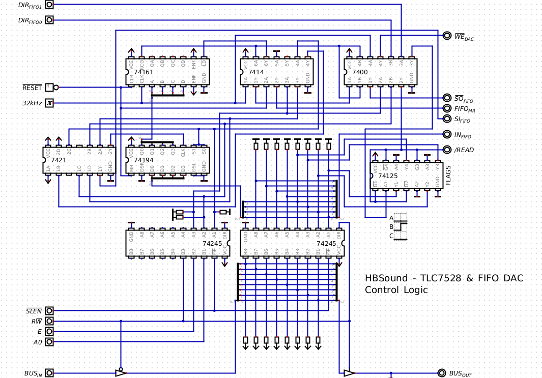
The control bit:
![]()
I spent a ton of time working on the control portion of the sound card. Several iterations of this design were assembled in H. Neemans Digital. I wound up going with this simplified design. I wanted to try to stick to discrete components that are mostly available still from digikey / Mouser - I could have most likely built the counter logic within a single or maybe to GAL's but for working with the parts I had on hand, and what I know I went with a Winbond W27E257 EEPROM as my only used / new old stock part. I had to use a 28c256 in the simulation but the actual part was the 12v eeprom. You can still get these in mass as pulls from 486 era PC motherboards on Amazon / Ebay and I have a ton -- I suspect many will also. The Fifo Selected is a standard CD74HC40105E, this allows the bit stream to be built in a buffer, which can give the programmer more time to do things while the slower DAC clock is shifting out the data. This technique was used in the famous (infamous? ) Disney Sound Source. Though, in that case a 555 timer was used to shift out the data at around 7kHz. The inevitable problem with this previous design is that the clock was inconsistent due to using a RC / 555 driven count (which would change the pitch off of a baseline), and many have argued that the similar COVOX sound adapter was a better solution as considerable better bit rates could be achieved even using a 8088 to control the timing.
Essentially the control piece does four things. First, it allows a set of flags from the 2 16 word FIFO's to be read by the user which allows the user to set the DAC bit rate between approx 7.2kHz and 32kHz in half step increments:
System CLK Sample Rt Dec Count HEX Count BIN Count OPCODE HEX Address For Bit 1843200 32000 56.6 38 0011 1000 00 38 16000 114.2 72 0111 0010 01 172 8000 229.4 E5 1110 0101 10 2E5 7200 255 FF 1111 1111 11 3FF this is set by sending a write to the memory mapped address of the interface +1 using the above OP code chart. The 3rd bit on the same address enables and disables the output of the FIFO (effectively halting the audio). For this I used a CD74HC194E Universal shift register, wired as a standard 4 bit register. A large reason for this is its load on high control, made the select logic for the overall build much simpler. (also I have a ton, waste not want not)
Second, the control system passively creates a DAC clock, using the system clock a pair of counters and an effective OR gate to or the System clock (E), with the counter reset signal which is determined by counting through a dirt simple FSM stored in the EEPROM. The reason the DAC clock has to be OR'd with the system clock is so that the FIFO shift out only occurs on the falling edge of the system clock, as the status flags of the registers are clocked into the d-latches on the rising edge of E. This asures the flags do not get latched while a shift out operation is happening, as the flags on the specific fifo are dual purpose depending on when you look at them.
![]()
Marked Vm - during this period if both the SO and DOR are low, the resulting reading is that the FIFO is "BUSY", however if it is still low, after the SO returns high, the resulting reading is "EMPTY". This was done so that multiple parts could be stacked together:
![]()
Third the control unit has a 2 bit latch which stores the NAND'ed flags from the two FIFO registers. The Flags being NAND'ed provide /DIR and /DOR from the two FIFO's. This latch is pulsed by the system clock (the fastest time domain on the system) so when read it should represent the status of the registers based off the most recent SI or /SO. The register is mapped to the base address for the device, and reading from it will deliver these results to the system bus.
The fourth simply allows latching values into the on board FIFO. I tried to keep all of the write functionality very similar to the DSS, so that people familiar with this interface can program its operation or port code that they've already written to this interface simply.
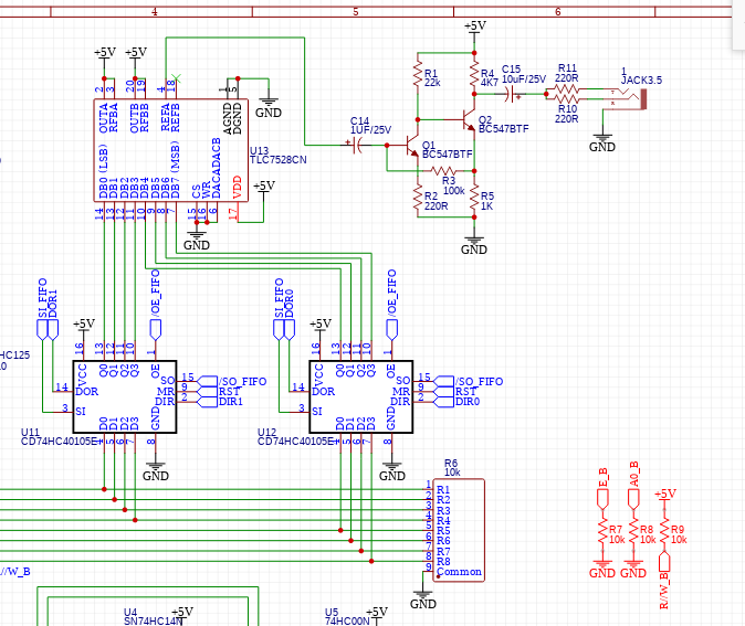
FIFO / DAC & analog section:![]()
The FIFO is different, the DAC is a discrete one, but from this point the sound card is basically a Disney sound source. The DAC hooked up to use +5V for both the Digital & analog source. Its likely this will cause some distortion from digital switching but I've tried to minimize by separating the ground planes:
![]()
I did end up building a discrete pre-amp, instead of the weird powered speaker bit that the DSS uses. Even on a bread board this provides a fairly noiseless line output for a set of amplified speakers I feel most people will be using. I did wire both the left and right channels on the line out to the single channel output I just used a simple divided resistor network. With a set of headphones hooked up the volume level seems comfortable to me. I put a few pads on the power and ground planes for the audio section to filter some of the noise but I don't think it will be needed. I kept all of the traces on one side to try to keep the planes as solid as possible (only in the audio section), this was mostly done for noise reduction end to end in the analog section. Obviously I will know more when i get the boards back from the manufacturer.
Thanks for those of you who stuck with me thus far. Today I will try to get all the project files updated. I am working with getting the boards for the initial prototype to the manufacture. There is a bit of a time crunch as we come up on lunar new year, which effects getting boards back quickly. If you come back later this afternoon (CST) they will possibly be up to date.Any questions or comments feel free to let me know what you think below or on Facebook. Thank you!
-
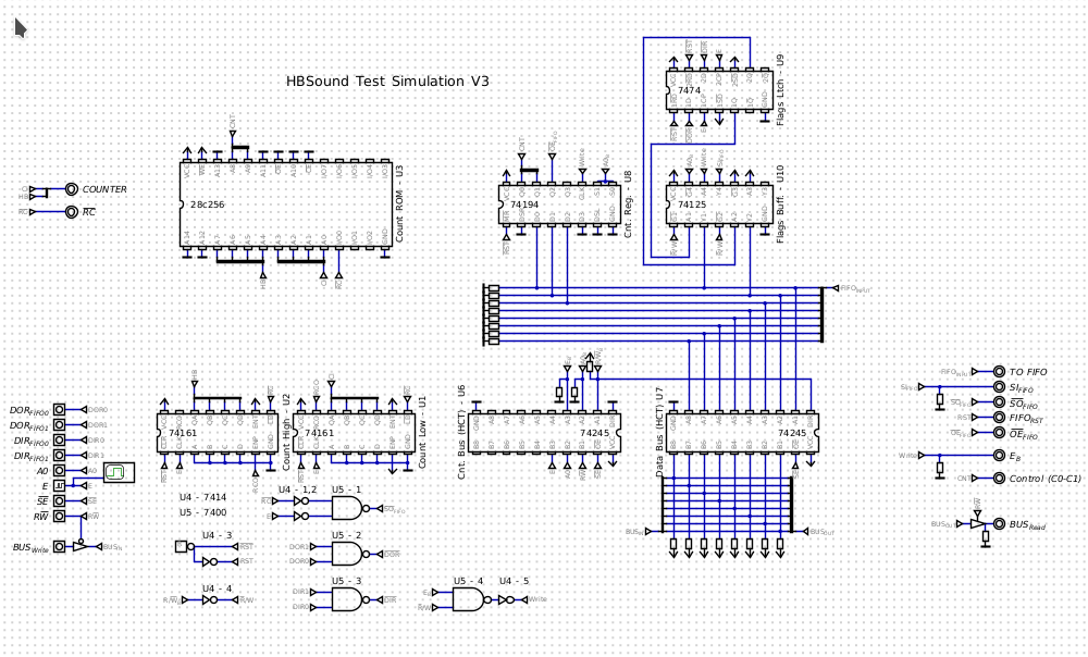
Simulations
12/02/2022 at 12:25 • 0 commentsThis week got crazy busy, still working on the sound card and I've mostly finished the simulations. some of them have a HC line to halt the main DAC clock. this was omitted in the final design for simplicity sake. take a look they are all built using "Digital" and uploaded into the files section.
"Digital" is a Logisim digital logic simulator by H. Neemann - though it is relatively hard to google the git hub due to the name. Fortunately, a conveniently provided link is above.
-
Prototype 1 issues, a second case study in optimizing failing process.
11/07/2022 at 03:38 • 0 comments![]()
Status:
HBSound development continues, Many have seen this picture kicking around social media. This is what I'm now calling prototype 1. And some of the things I learned from this build are its complexity is it's downfall. When I built the top module I felt it was reasonably successful jumping point because it actually worked. This led me to add in more complexity and, I believe that where the issues started. Prototype 1 used a large NAND to combine all of the output signals, and the ready signals (plus some select able buffered clocks) to make the shift out clock. For a lot of reasons this was a bad Idea. in fact the design was so busy, and chaotic I am hesitant to share it further than the block diagram because, I am afraid in doing so I open up opportunity to optimize a thing which probably is so flawed it should not exist. That being said, in prototype 2 I have to go so much simpler. The first issue is the SN76489, its a wonderful part for its time, but it has some issues which require layers of complexity to over come. Firstly it requires a 3.5-4 MHz clock to create compatibility with period correct machines, most of the source music is written with this timing range in mind and so its a requirement if you want to play music files from other machines that also have this sound chip. The part also has to be silenced from the host machine using initialization. Until then it comes up in a random state and makes noise out of the output. To over come this typically a SR flip flop is used to gate the PSG's clock, this requires more control logic and additional logic to XOR the system reset line which again adds more complexity. This set up allows you to halt the PSG clock but this does not completely reduce the noise from the PSG. The other issue was trying to use the FIFO in a pseudo write - through mode this failed. The timing window was too small, too many signals had to settle in the gate, this created among other things, unreliable timing.
So where does that leave us?
I think I need to take a look at picking one chip for the card and I'm leaning widely towards the DAC. A DAC provides the ability to create very robust sounding output, with digitally generated tracking using spare cycles between operations; there's a large body of sample work as the design I'm shooting for is very compatible with the COVOX / DSS for the PC only with a beefed up oscillator design. Another big benefit is the part is still available on Mouser / DigiKey. The PSG has complications which make it harder to use reliably, requires gated clock generation, that has to be halted to really effectively use it as a select able module, the part also has to be pragmatically silenced in order to really shut down the sound generation completely. Another issue which is a small problem since they are still plentiful the PSG is new old stock.
I think the choice is clear, I should use a single chip DAC and stop messing around with trying to provide a optional write through mode. The 2-32 kHz sample rate (which is software select-able) I'm shooting for is more than enough to produce far better sound quality than even the reference Disney sound source, which had a fixed 7-8Khz sample rate provided through a 555 timer. My design uses a fixed crystal oscillator to produce the base clock and a counter chip to produce the pulses.
I decided this time to build up the control logic in "Digital" logic simulator. Its a nice Logisim clone, that's actually got properly functioning 74254 bus transceivers, which i used HCT variety in my build so I could use faster HC logic and still interface a TTL CPU. You will recognize the Motorola specific architecture signals are used here but the basic design should be able to be adapted to any basic single clock R//W set up.![]()
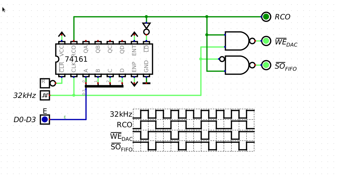
The control logic is 8 chips, most of witch is dedicated to creating the two falling clock edges needed to clock the DAC and the shift out line of the FIFO. Here is a blown out diagram of the functionality of this clock generator:
![]()
The 4 bit value is loaded into the counter via a universal shift register. The register is wired as a storage register. I used a universal shift register because its Load operation is a high signal on both control pins, which makes building the logic to select which device gets clocked on a write operation much simpler. The basic thing to get your head around and understand is, it provides a parallel 4 bits to the inputs of the counter, and can be set by sending a value to Slot enable + 1 (we abbreviate as SLEN). A quirk of this design verses using a state machine is the active count simply counts up from the set value but only after it is latched in, and that means if a count is started the new value is only valid only after the pulse generation happens. So a programmer will have to wait for the first cycle to pass by burning some cycles to grantee the clock is counting at the desired rate. Once interrupt generation is more clearly defined it will be easier to determine how this looks.
We do a NAND operation on the RCO with 32kHz & /32kHz, the result is 2 falling clock edges on the rising and falling edge of RCO. First we sample the waiting output on the FIFO which is always the current byte needing to be read in, by clocking the DAC, then on the rising edge of the DAC clock we shift out the next byte from the FIFO.
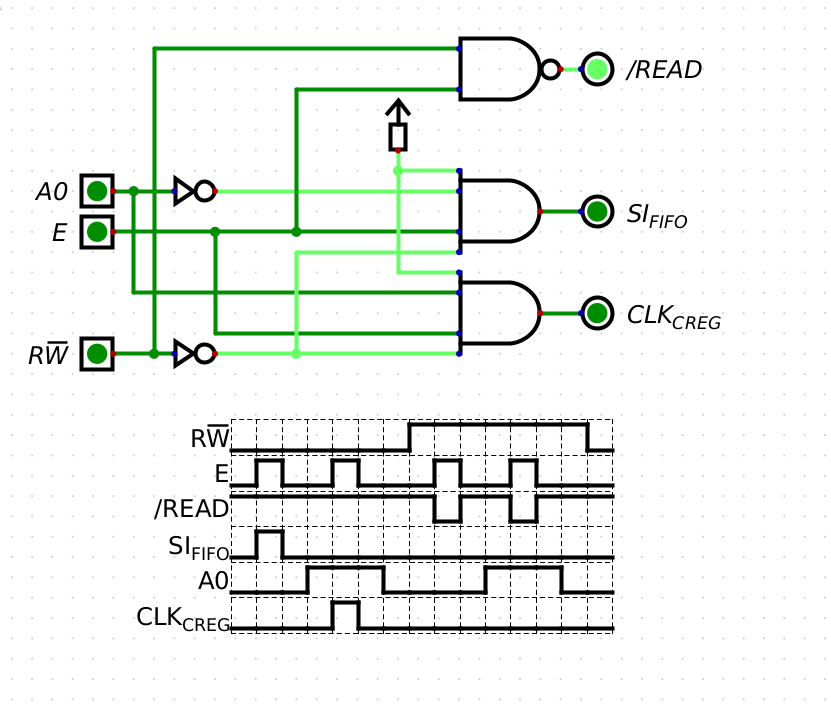
Then I use a 74HC21 and a spare NAND gate, and 2 more inverters to generate the /READ, SI_FIFO, and CLK_CREG signals (not pictured on main diagram but wired to the clock pin on the universal shift register).
![]()
These signals are buffered at the card edge, by a locked direction bus transceiver (the data bus direction on the transceiver for the main bus). the transceivers normalize the TTL signals on the system bus and control lines to a more normal CMOS levels. Oddly enough the Shift in, signal for the FIFO is positive edge triggered, while the shift out signal is falling edge triggered, this was slightly advantageous as the universal shift register is also positive edge triggered.
Buffering the signals and gating the clocks with R//W adds the needed delay to properly clock the data bus in generally a stable state as:
6809 notes
 this is a relatively over simplified assertion but typically in a
 minimal controller based set up:

"e" line goes low ...
 step1                    {address bus updates (addressed transceiver
                          {should turn on if any)
Almost at the same time   {
                          {r//w line (transceiver direction changes
                          {depending on configuration)

   at the end of this transitional step the above signals are in a steady
   state and break down at the next low e transition.


 step2                    {data bus is asserted fractions of a second
                          {before ...
Almost at the same time   {
                          {"{e" line goes high (/write /read at this
                          {point when NANDED with R//W)

  at the end of this transitional step the above signals are in a steady
  state until the end of the next step1 both step 1 and step 2 are at
  in the same states from the end of step 1 until the next
  q pulse (90 degrees later)

while....

q goes high 90 degrees later from e. at approximately the same time as
the step1 and step2 transition

(see diagram on page 9 of the datasheet)

DMA, HALT and other bus control scenarios not taken into account.
Reading out the flag:
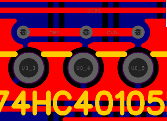
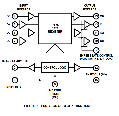
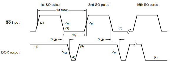
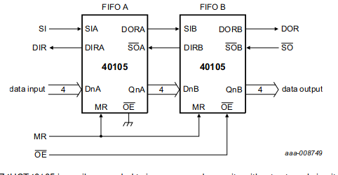
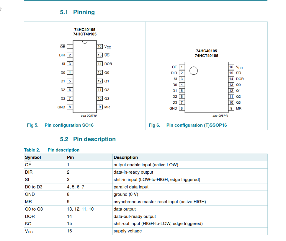
The /READ signal turns on the flags buffer, which currently outputs the NAND of DIR_FIFO0 & DIR_FIFO1. these values are internally latched within the FIFO. This works without the addition of a second latch as the value is valid after the falling edge of the last SI_FIFO signal, which is the case one clock cycle (at least) of E later, when the next /READ signal is asserted. For the interested here is a breakdown of the 74HC40105 FIFO:
![]() The downside to this means the DOR signals, would absolutely need control logic that would only make the DOR valid to the flags buffer only after the rising edge of the /SO_FIFO signal. Additionally the signals from both chips would have to be fed from an AND gate, as both the DOR and DIR pins go low for a moment as the internal bubble up happens. While this period is fast enough for it to fall between clock cycles from either end of the chip its slightly more difficult due to the way /SO is clocked. Since the input is handled by the system clock the currently latched FIFO value is guaranteed valid because it is impossible to both read and write to the card at the same time, this is not the case with the output side of the FIFO, as it is driven from a separate clock which operates at a much slower rate, that is variable and a trialing pulse to latch the value is not always guaranteed. Generating a latch clock would be tricky as it would need to come after the value on DOR is valid as a buffer is empty signal (vs busy). Simply latching a 74hc74 using the buffered rising edge of /SO_FIFO might work; I may play around with this, as I have at least 2 spare buffers and adding a 74HC74 at this point is trivial. I also intend to generate 2 interrupts from the card, one 32kHz interrupt and one off of the buffered DOR signal from the FIFO. These interrupts will be re-direct able into the IO/interrupt channels on the HB6809 or simply switched off completely.
The downside to this means the DOR signals, would absolutely need control logic that would only make the DOR valid to the flags buffer only after the rising edge of the /SO_FIFO signal. Additionally the signals from both chips would have to be fed from an AND gate, as both the DOR and DIR pins go low for a moment as the internal bubble up happens. While this period is fast enough for it to fall between clock cycles from either end of the chip its slightly more difficult due to the way /SO is clocked. Since the input is handled by the system clock the currently latched FIFO value is guaranteed valid because it is impossible to both read and write to the card at the same time, this is not the case with the output side of the FIFO, as it is driven from a separate clock which operates at a much slower rate, that is variable and a trialing pulse to latch the value is not always guaranteed. Generating a latch clock would be tricky as it would need to come after the value on DOR is valid as a buffer is empty signal (vs busy). Simply latching a 74hc74 using the buffered rising edge of /SO_FIFO might work; I may play around with this, as I have at least 2 spare buffers and adding a 74HC74 at this point is trivial. I also intend to generate 2 interrupts from the card, one 32kHz interrupt and one off of the buffered DOR signal from the FIFO. These interrupts will be re-direct able into the IO/interrupt channels on the HB6809 or simply switched off completely.
Whats next?
Next is the build up of the prototype, I may jump right to spinning up boards for the sound card after I'm confident I can control the DAC using 5 Volts only. So I guess the fist step is getting the breadboard cleared off of the first prototype and hooking the DAC to a micro controller to try to build the analog circuit and get that working. -
The plan so far.
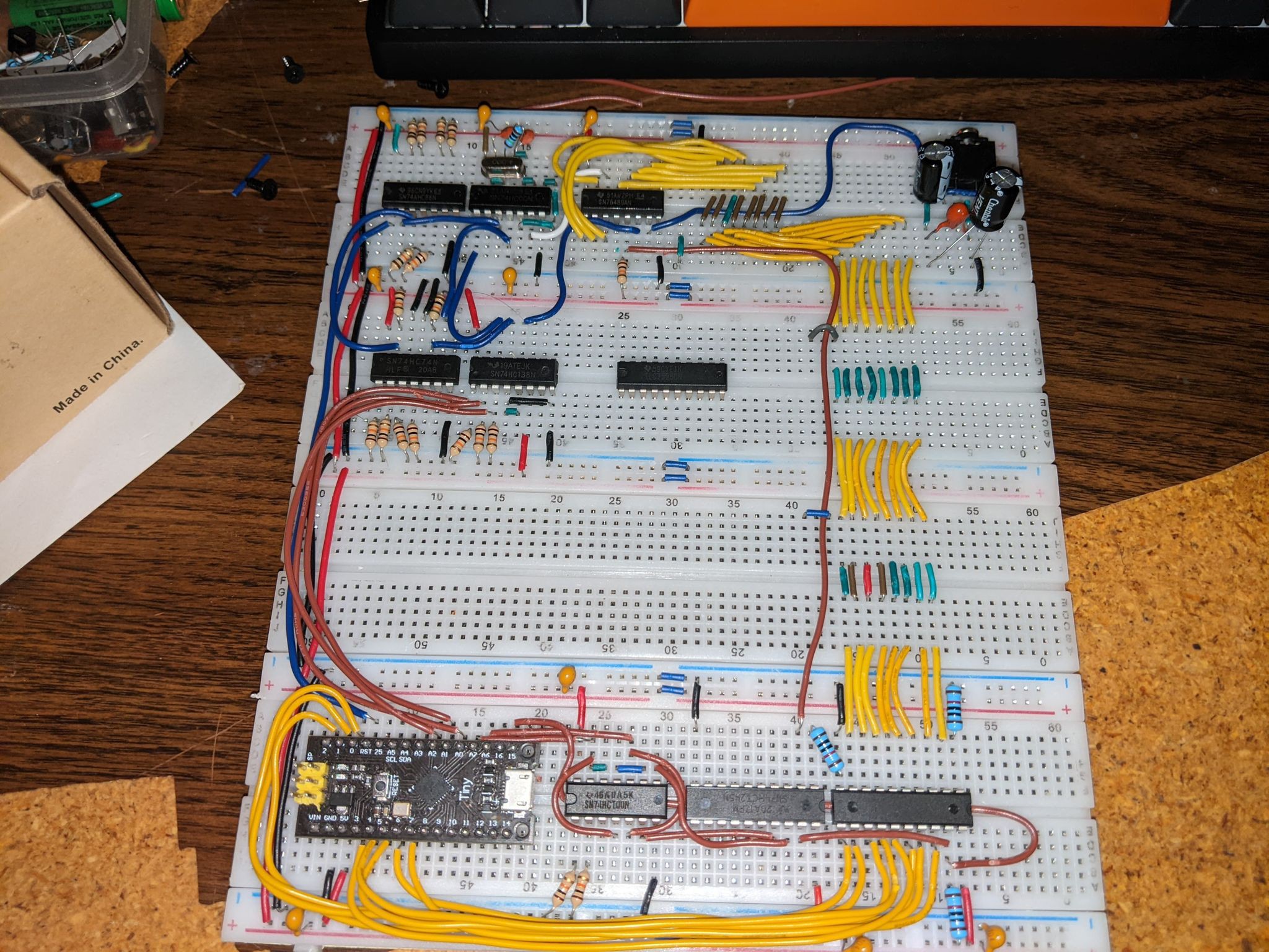
10/26/2022 at 03:29 • 0 comments![]()
So for starts I am building a rough bread board prototype, which i can control with a easy to program attiny88 dev board ( I use a cheep USB programmer as the usb ports on these are practically worthless.) I can run a simple test program at the moment that sets the registers in the PSG (using the control logic on the bottom board (all HCT). Next is to hook up the FIFO module, and get it to do write through:
- Write through will pass along the current data to the PSG / DAC immediately following the rising edge of /WRITE signal from the control logic.
- The buffer will hold the data only if the PSG or DAC are not ready to receive the data (which at normal speeds wont likely be more than a clock cycle.)
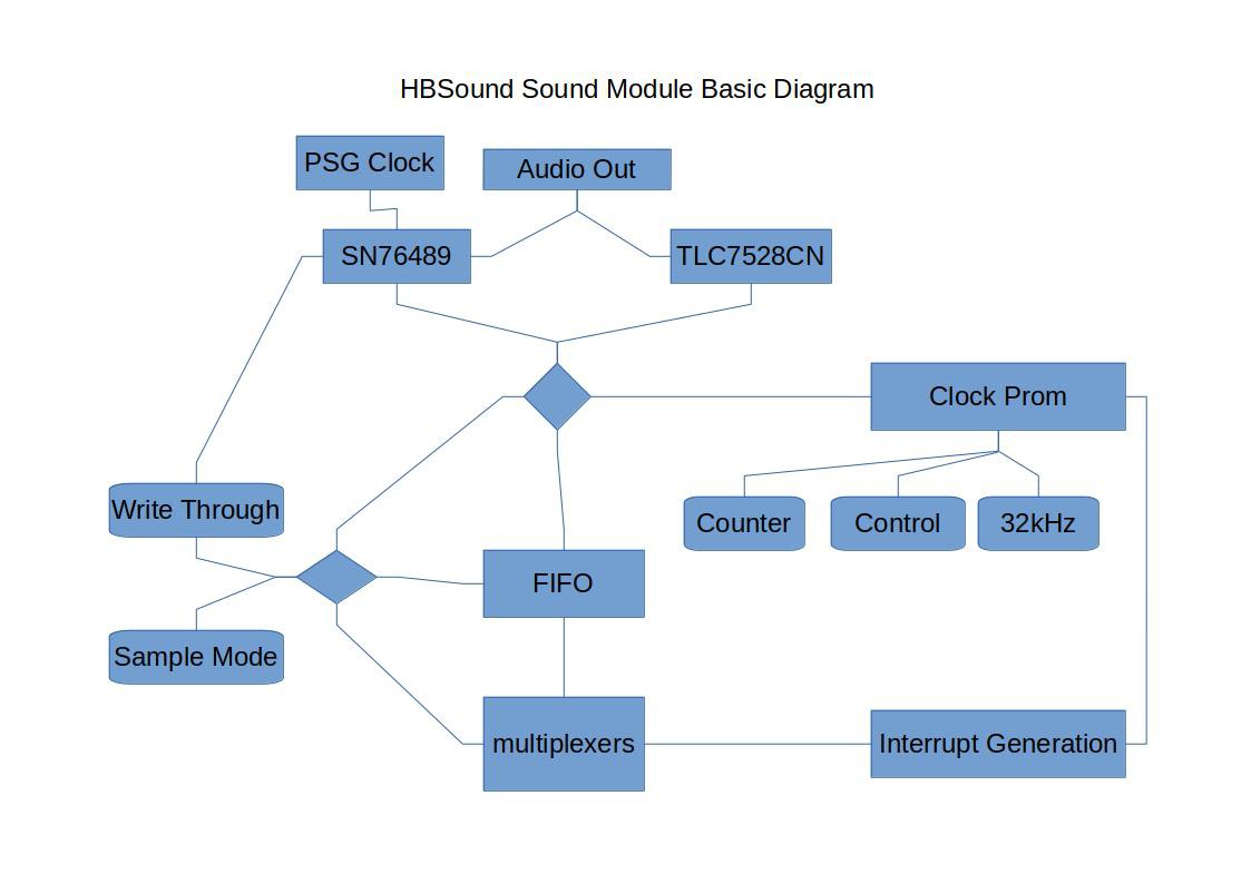
After that is working, I will start work on a design to implement an adjustable clock, with interrupt generation as an option that can be used to set a sample rate based on a maximum of 32 kHz. The basic diagram for the card is as follows:
![]()
The design is still fluid, but I am hoping once I get the kinks worked out of write through I should be able to proceed on to getting the TCM (Timer / Clock Module) finished.


 The downside to this means the DOR signals, would absolutely need control logic that would only make the DOR valid to the flags buffer only after the rising edge of the /SO_FIFO signal. Additionally the signals from both chips would have to be fed from an AND gate, as both the DOR and DIR pins go low for a moment as the internal bubble up happens. While this period is fast enough for it to fall between clock cycles from either end of the chip its slightly more difficult due to the way /SO is clocked. Since the input is handled by the system clock the currently latched FIFO value is guaranteed valid because it is impossible to both read and write to the card at the same time, this is not the case with the output side of the FIFO, as it is driven from a separate clock which operates at a much slower rate, that is variable and a trialing pulse to latch the value is not always guaranteed. Generating a latch clock would be tricky as it would need to come after the value on DOR is valid as a buffer is empty signal (vs busy). Simply latching a 74hc74 using the buffered rising edge of /SO_FIFO might work; I may play around with this, as I have at least 2 spare buffers and adding a 74HC74 at this point is trivial. I also intend to generate 2 interrupts from the card, one 32kHz interrupt and one off of the buffered DOR signal from the FIFO. These interrupts will be re-direct able into the IO/interrupt channels on the HB6809 or simply switched off completely.