Close
0%
0%

HB6809 Homebrew computer

This is my 6809 Homebrew Computer

Similar projects worth following
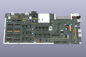
I've built an expansion computer, based on Grant Searle's / Jeff Tranter's Minimal 6809 computers. The computer has 4 expansion slots, an expanded memory map, upgraded power distribution and expanded experimentation area.

I wanted a low cost kit like computer based around the 6809, with a very simple expansion bus.

Design goals:

  1. Cost - try to keep board footprints small (this was hard, further minimization with surface mount parts would be the way to go even lower)
  2. Minimal - keep the focus on simplicity, very few chips and very simple memory map
  3. Extendable - break out as many test points as practical and in locations that make them easy to bodge to.
  4. Runs existing firmware - Since I plan to use this as a learning platform I want the computer to be built around a reference design 
    1. Grant Searles Page : http://searle.x10host.com/6809/Simple6809.html
    2. Jeff Tranter's page : http://jefftranter.blogspot.com/2019/01/a-6809-single-board-computer.html
  5. Open hardware (CERN-OHL-P) -- a text copy is in the files section if this link is ever bad.

Liability / warranty language from the license

5.1 DISCLAIMER OF WARRANTY -- The Covered Source and any Products are provided 'as is' and any express or implied warranties, including, but not limited to, implied warranties of merchantability, of satisfactory quality, non-infringement of third party rights, and fitness for a particular purpose or use are disclaimed in respect of any Source or Product to the maximum extent permitted by law. The Licensor makes no representation that any Source or Product does not or will not infringe any patent, copyright, trade secret or other proprietary right. The entire risk as to the use, quality, and performance of any Source or Product shall be with You and not the Licensor. This disclaimer of warranty is an essential part of this Licence and a condition for the grant of any rights granted under this Licence.

5.2 EXCLUSION AND LIMITATION OF LIABILITY -- The Licensor shall, to the maximum extent permitted by law, have no liability for direct, indirect, special, incidental, consequential, exemplary, punitive or other damages of any character including, without limitation, procurement of substitute goods or services, loss of use, data or profits, or business interruption, however caused and on any theory of contract, warranty, tort (including negligence), product liability or otherwise, arising in any way in relation to the Covered Source, modified Covered Source and/or the Making or Conveyance of a Product, even if advised of the possibility of such damages, and You shall hold the Licensor(s) free and harmless from any liability, costs, damages, fees and expenses, including claims by third parties, in relation to such use.


Support the Project:


10% of your order will go back into covering the cost of prototyping, parts and other materials for creating new and interesting projects for me to write about. Including new modules for the HB6809

Launch Video:


Build Files: 

Github  -- My Github for the HB6809

Build Recommendations:

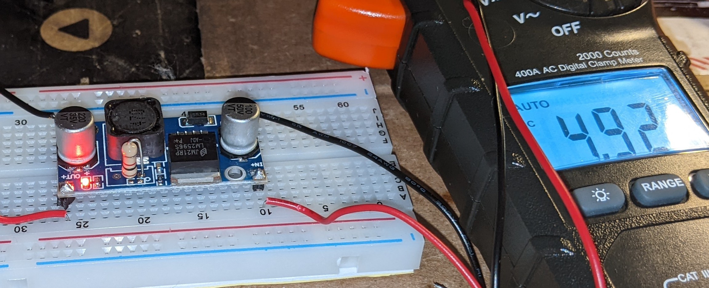
For the LM2596 DC to DC Converter module, It may be prudent to put break away pins (like used in a standard header ) on each of the four corners to prevent the module from shorting on the board.  Additionally if you choose to remove the variable resistor from the module I found a standard through hole resistor (1K %5) provides a near perfect 4.9V  you can simply mount it in the two holes that are laterally located next to the SMD pads that are revealed when you pull the variable trim pot from the board. 

Optional power module mod:
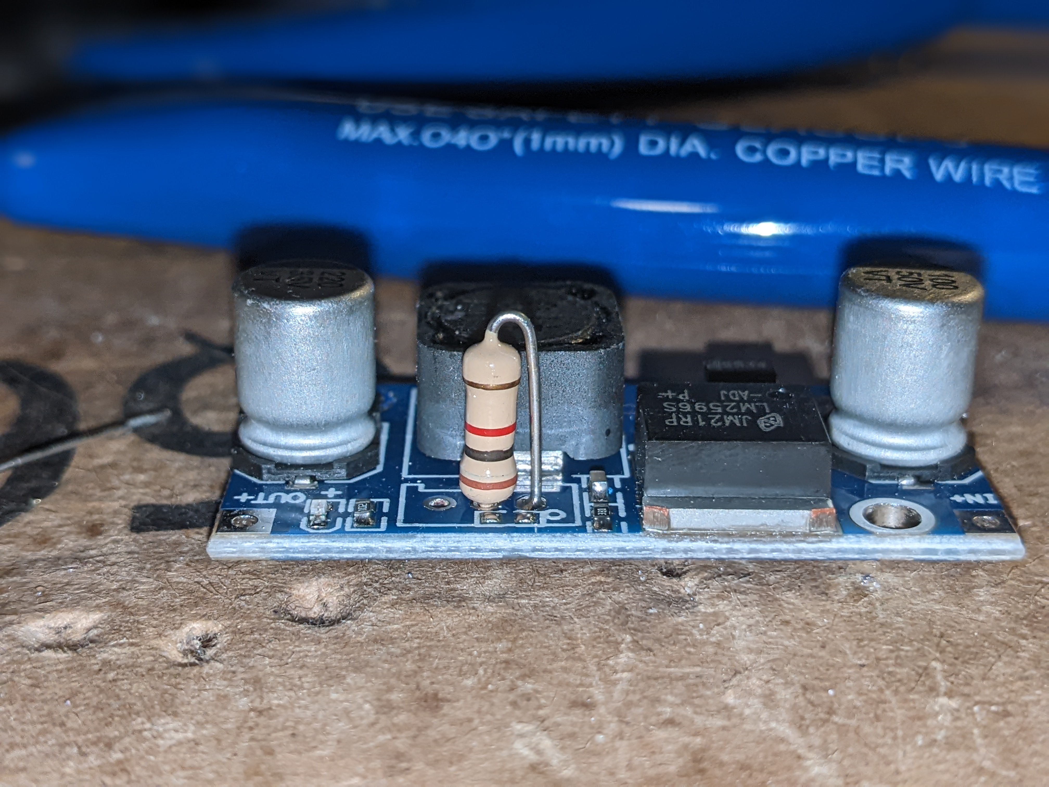
Stand offs installed to prevent board from shorting:
HCT vs LS considerations:

I've used HCT logic chips in my design, you can build this with LS, but the fan out implications are considerably more dire. particularly with  the address decode lines being tied directly to the two 74 series chips.   Pay particularly close attention to the 6809 datasheet in this area, remember, HCT gates draw considerably less current from the bus, and since these decode gates are directly connected to the bus this will change those...

Read more »

Updated Combination ROM.7z

Updated ROM File / Jeff Tranters Combination ROM with a larger contiguous RAM space - This is released under the Apache License

x-7z-compressed - 108.40 kB - 02/06/2023 at 06:27

Download

BOM.TXT

updated bom

plain - 2.28 kB - 09/20/2022 at 18:27

Download

cern_ohl_p_v2.txt

Open Hardware Licence

plain - 8.64 kB - 09/15/2022 at 04:36

Download

HB6809 Minimal ACIA EasyEDA Backup File.zip

Back up of the entire EasyEDA from around V2.2 of the main board PCB

Zip Archive - 105.71 kB - 09/15/2022 at 03:59

Download

Gerber_PCB_HB6809.zip

Main PCB Gerbers

Zip Archive - 356.90 kB - 09/15/2022 at 03:59

Download

View all 12 files

  • 1 × 68B09 CPU A Motorola or second source compatible 6809 CPU (this is not to be confused with the 6809E or EP )
  • 4 × SIP-9 (BUS Type) 10k Resistor networks these tie each 10k path through pin 1
  • 5 × 10k Resistor 5% or better 1/4 or 1/2 Watt Footprint uses 1/2 watt but they are not required
  • 4 × 1k Resistor 5% or better, 1 is for optional power module mod, 2 for the optional serial card and may be omitted (1/2 or 1/4 Watt)
  • 1 × SN74HCT00N Logic ICs / Gates and Inverters

View all 26 components

  • Working on Jeff's Combination ROM / W27E257 Tests & CMOC

    Dave Collins02/05/2023 at 19:36 0 comments

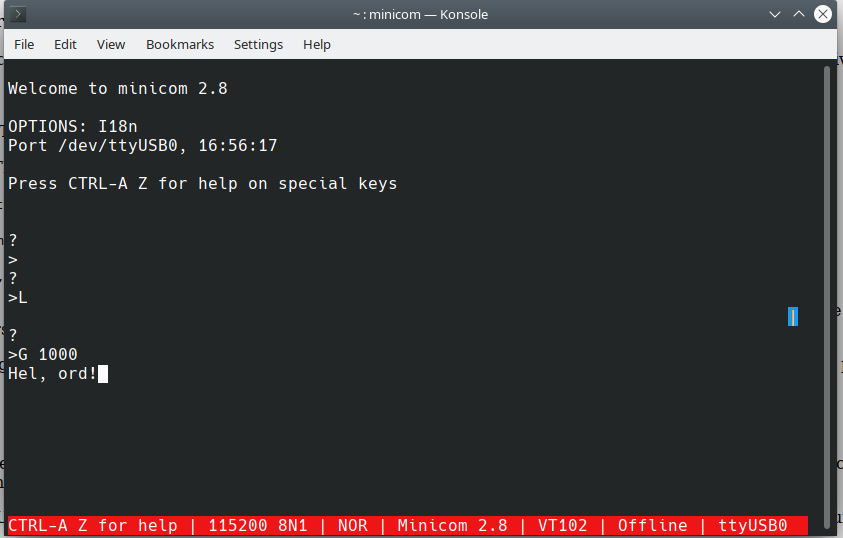
    Hel ord
    it's not Hellorld... but so close

    So it's been a while how about an update?

      I have been working towards a number of projects lately including a interesting series (i think) on the ZX81 that I am working on, as well as HBSound my 8 bits sound card similar to the Disney sound source (with a beefed up sample clock circuit).  I landed on trying to get CMOC fired up on the HB6809 to a state that I can start writing some faster code (using a c like compiler).  The best part of this hobby is that you can really get lost in the minutia of the varied areas of home brew computing.  This week was software; and like so many things I really threw myself into it.

    Really putting your foot in it:

      So if its not obvious, I am an autodidact when it comes to hardware design.  I try to test everything and build safe functional circuits that are close to the lower speed designs of the 70's and 80's, but  a lot of this is experimentation and keeping a solid notebook of what I think is going on.   I believe what Ive built in the HBSound is just about the best design I have ever made. However, what I lacked at the end of the project was a really good way to test the sound card at speed.  Enhanced basic is not really fast enough to write the buffer and produce anything further than a 200hz tone, and I am a complete novice when it comes to 6809 assembly (I know just enough to be really dangerous).  I am however proficient in C, specifically the flavor or C that was kicking about in the early  90's on 16 and 32 bit CPU's.  I also know a fair bit of Pascal, as well as some 8080 assembly language.   There exists a c like cross compiler for the 6809, called CMOC, it's very similar to C, and produces .srec files with little issue for quick loading over serial. 

      I set out to get CMOC,  to produce working machine language that Assist09 can load.  In an effort to facilitate this I had to figure out how to re-direct a minimal amount of the standard library to support the ACIA at A000.  The manual for CMOC actually is fairly comprehensive and includes a section on doing specifically this.  Additionally ASSIST09 has a few system calls that allow for things like sending a character and reading from the terminal a snap:

    *******************************************
    * ASSIST09 MONITOR SWI FUNCTIONS
    * THE FOLLOWING EQUATES DEFINE FUNCTIONS PROVIDED
    * BY THE ASSIST09 MONITOR VIA THE SWI INSTRUCTION.
    ******************************************
    INCHNP  EQU     0               ; INPUT CHAR IN A REG - NO PARITY
    OUTCH   EQU     1               ; OUTPUT CHAR FROM A REG
    PDATA1  EQU     2               ; OUTPUT STRING
    PDATA   EQU     3               ; OUTPUT CR/LF THEN STRING
    OUT2HS  EQU     4               ; OUTPUT TWO HEX AND SPACE
    OUT4HS  EQU     5               ; OUTPUT FOUR HEX AND SPACE
    PCRLF   EQU     6               ; OUTPUT CR/LF
    SPACEF  EQU     7               ; OUTPUT A SPACE
    MONITR  EQU     8               ; ENTER ASSIST09 MONITOR
    VCTRSW  EQU     9               ; VECTOR EXAMINE/SWITCH
    BRKPT   EQU     10              ; USER PROGRAM BREAKPOINT
    PAUSE   EQU     11              ; TASK PAUSE FUNCTION
    NUMFUN  EQU     11              ; NUMBER OF AVAILABLE FUNCTIONS

    We can call these by simply entering a software interrupt followed by a byte describing the function we'd like to do (very similar to a BDOS/BIOS call in CP/M.)  Armed with this knowledge I set out to build a output routine for CMOC that would use some of these routines to see if I could get the terminal to output an obligatory "Hello, World!" program.

    The obligatory "Hello, World!" program:

     Before I discovered the system calls in assist09 I found you could output characters to the terminal by simply writing to A001, the main issue with this is that this process requires either a programmable interrupt and a buffer to handle waiting for the appropriate time when the ACIA is ready for data to output --- OR a subroutine that scans and waits for the register in the ACIA to show that it is ready (by returning 0x2).  If you simply send the character data to the interface you will find it will drop characters (like the picture...

    Read more »

  • Final Build PCB V2.2

    Dave Collins09/14/2022 at 05:11 3 comments

    UPDATE: Thanks to an insightful comment by Doug Merrett You CAN relocate the board ID on boards produced by JCLPCB using the following directions.

    Its finally here!

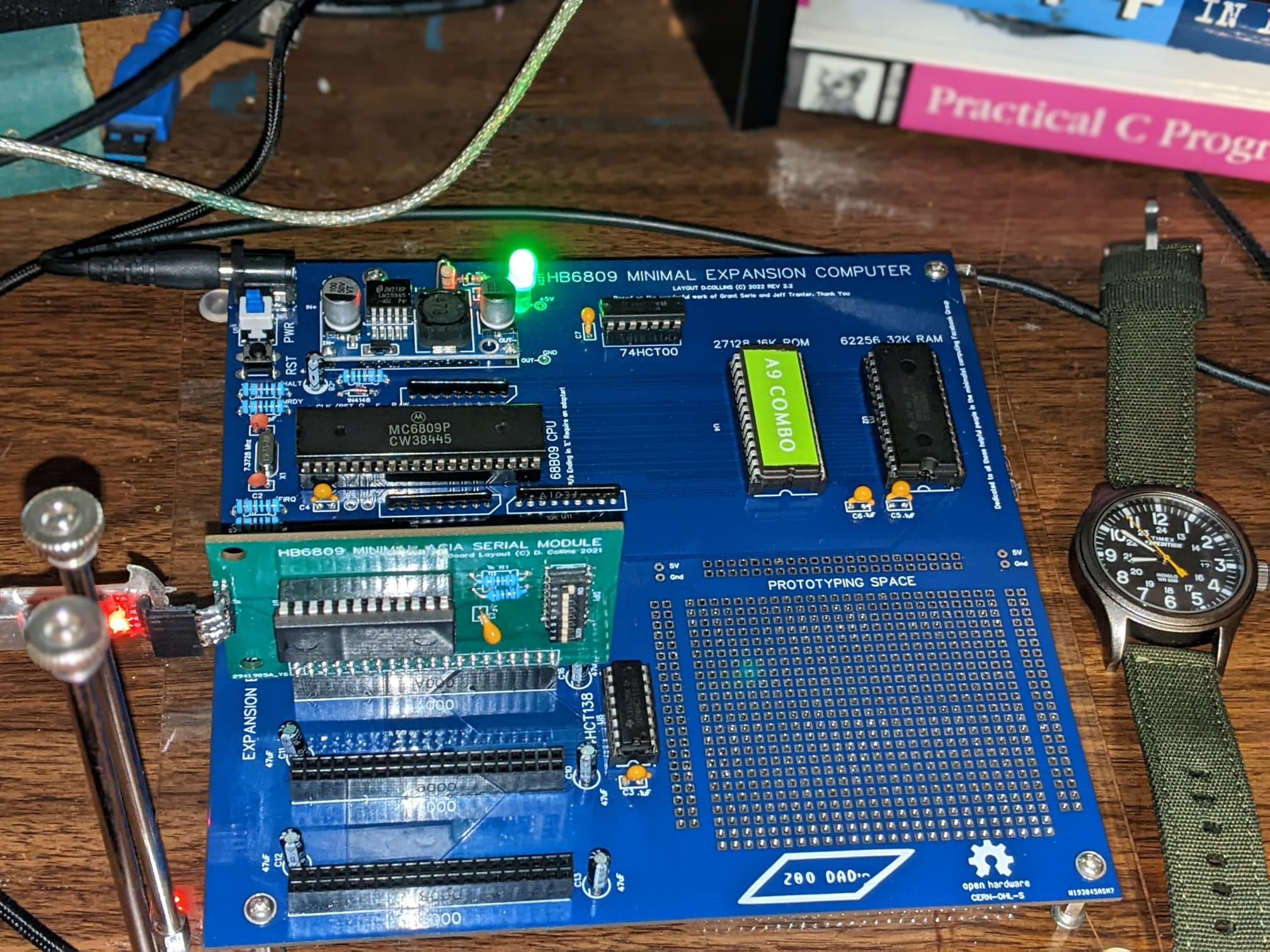
    As of today, I am considering the main build complete.  There's still quite a bit of work to do in making some fun optional modules for the computer, but I am comfortable releasing the build files to the general public for anybody to try out.  It has been a ride for certain!   I wanted this to be a fast, no-nonsense project. here we are roughly 2 months out start to finish.  I can't even believe it myself, back in July I didn't think I'd get this far by now but it's basically a complete project.  If anything, this really has been the pallet cleanse I needed after coming off such a complex build that, in the end there wasn't much in the way of results. What a relief to finally be here.

    Final Road blocks and hurdles cleared:

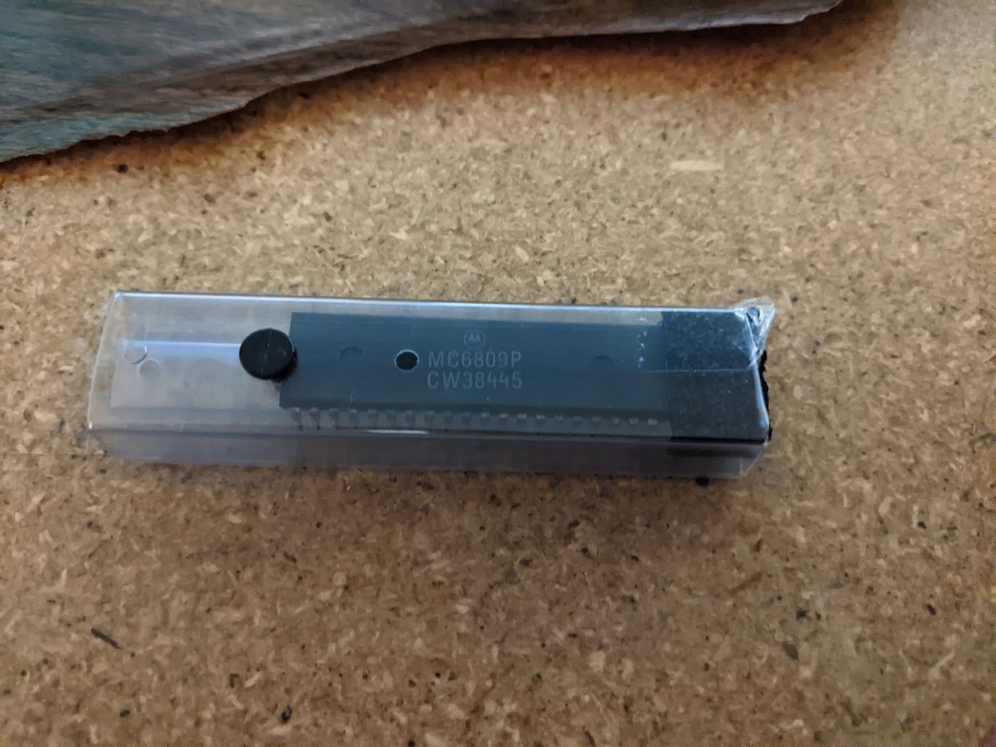
    if you've been following the build on Facebook, then you'll know I made a slight mistake during final assembly, resulting in some parts being damaged.  If you compare the two boards assembled in pictures then you will see that I have a bog standard Motorola (45 week of 1984)  6809, instead of the proper speed grade 68B09, which the board calls for.  I've since ordered the right CPU's from a recycler in Texas and they should arrive soon.    The issue came in when I was getting ready to test the lines with the scope, I forgot that I had the board powered on, and when I went to solder the lug to the ground pin on the power supply module, something happened (I still don't know what, but I'm in process of doing some testing to determine exactly what).  As soon as the soldering iron tip hit the pin on the module the voltage on the 5V line spiked the LED got very bright and I managed to fry out my circa early 2000's 6809 chip, a vintage eprom, and a hand full of  TI 74HCT chips.   I suspect that it may have to do with my soldering Iron not being isolated properly but also could be simply that the module is not designed to be soldered to while its in operation, the end result was I had to burn a new EPROM and switch out the CPU for the other one in my collection.  It's running happily clocked twice it's rating; I won't run it this way for long but I wanted to make sure the final boards were working before releasing to the public.

    I made a small change to the DC-DC converter module, I removed the high turn potentiometer and replaced with a standard 1/2 watt, 5% 1K ohm resistor.  This provides a steady 5v output, without the worry of the pot becoming scratchy, getting bumped or turned.  It's absolutely optional but since it was a very easy mod to make I did it because it's some piece of mind really.  If you look closely you can see there's a SMD pad which essentially routes to the same location as the through hole pads, so that you can use a simple SMD resistor (it absolutely doesn't have to be 1/2 watt tolerant, this is just what I had on hand ).

    V2.2 of the PCB - PCBWay / JCLPCB PCB Comparison:

    I will start out by saying, I am looking at these boards like a hobbyist would.  I'm not a quality control engineer, so I can only write what  I see but the question does get asked, Is the higher price of PCBWay from start to finish for a plated through hole HASL 2 layer board worth it?  I think the short answer is yes, but let me spell out a few of my observations so you can get an Idea of what I am seeing.  I should also point out, PCBWay, our build sponsor has covered the cost to fabricate the final test boards, However they aren't reviewing my thoughts or requiring me to say anything in particular in my review, what follows is simply my honest opinion on what I see between the two boards.  

    Finish (Solder mask): 

    JCL's solder...

    Read more »

  • Prototype Layout 2.1

    Dave Collins08/28/2022 at 20:24 0 comments

    Update: PCBWay has kindly offered to sponsor the cost of the next run of boards! This is amazing, as I was planning on doing a comparison between JLC and PCBWay in my next post. Follow this space for more soon!


    The boards: 

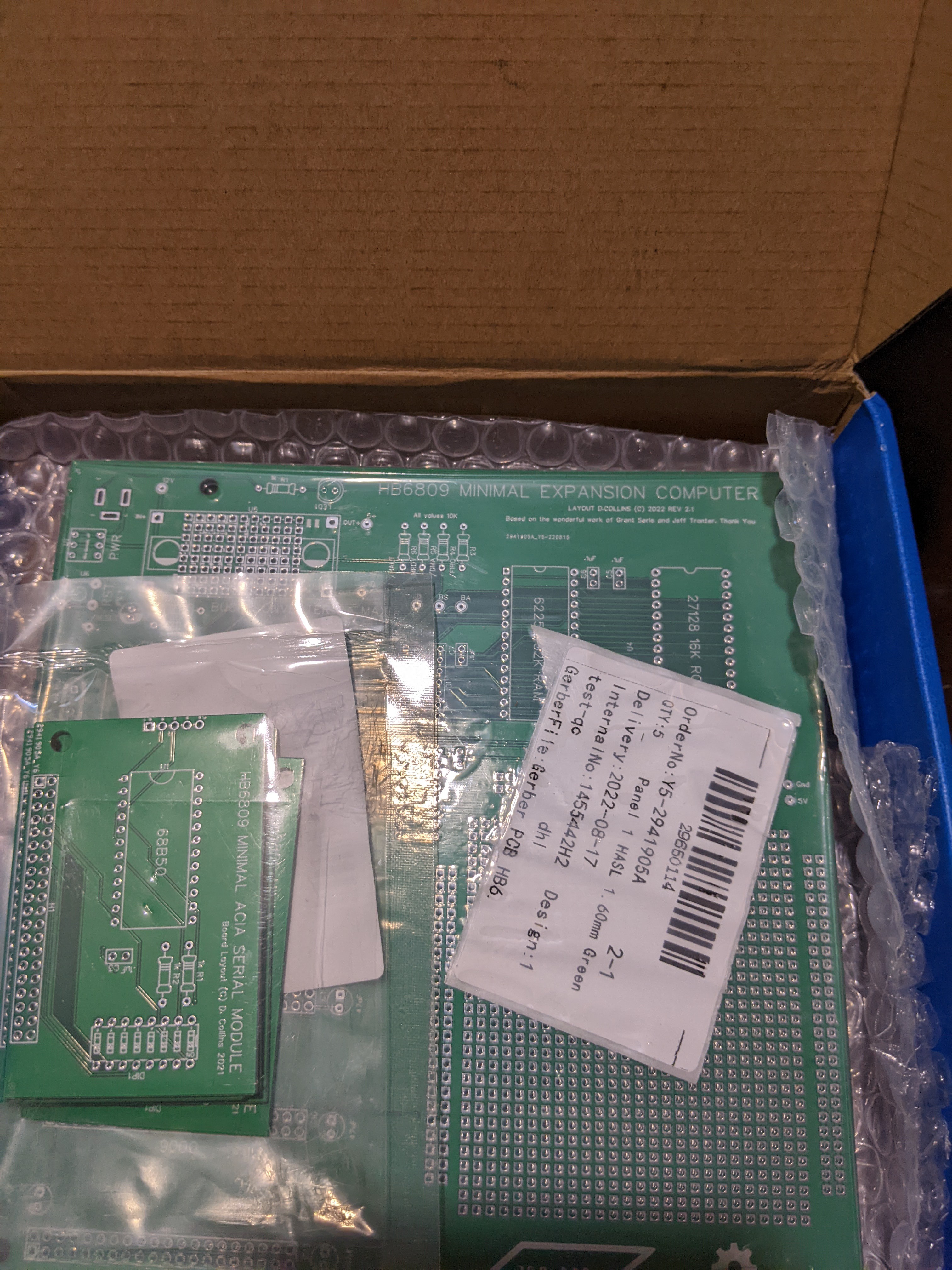
    The Boards Were received when the manufacturer stated they would be here. Both the AICA board and the main PCB were packaged with care, there was minor shipping damage to the box but the goods came unhindered inside the packaging. This shipping damage was just slight box crumpling, that could be more blamed on the shipper DHL, than anyone but to be honest I've received things from amazon in far worse shape.

    Fixing the Issues:

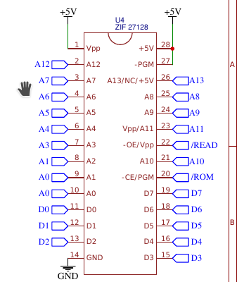
    After buildup, the main PCB had some issues. The first big problem I ran into was the addressing on the schematics (which in turn translated to the layout) for the EPROM:

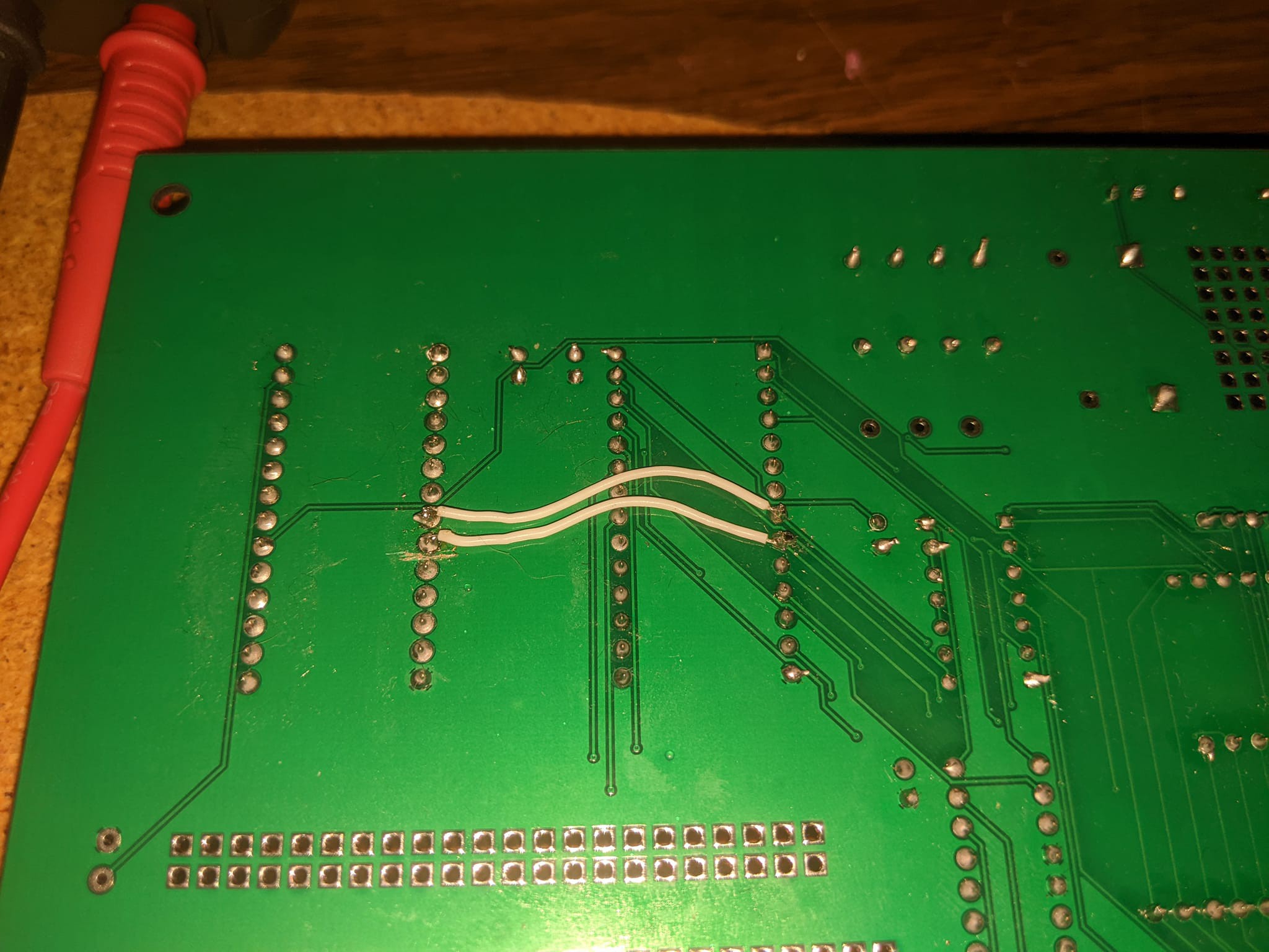
    As you can see the A0-2 have potential issues.  When i probed the R//W line coming from the CPU with the scope looking for issues I determined that it was basically at it's high state, essentially just reading and probing through the address lines.  Upon checking the decode logic I found this to be the case as the selector would simply run through the selected lines over and over again.  Fortunately, this wasn't hard to fix, I simply cut the two traces (one between pins 10 and 9, and the trace going A1 on the ram running from pin 8.)  Then after that was done I bodged the two pins with silicone jacketed flexible patch wire.

    After doing this I got much more normal r//w readings with every so often it switching between the two signals as it processed through the loop for the machine language monitor.   The other issues were a handful of silly auto-router related mistakes such as a few lines running through a plated through hole section and the +5V and GND nets being routed throughout  the project because when I went to finish up the remaining routing with the auto router I forgot to select them to skip the routing.

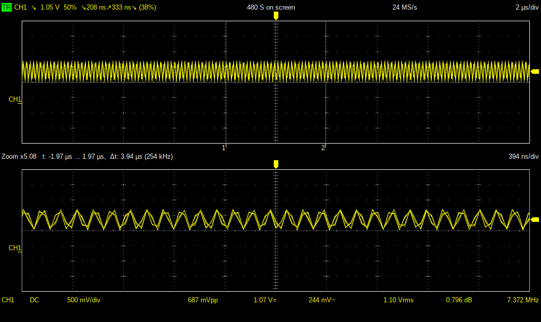
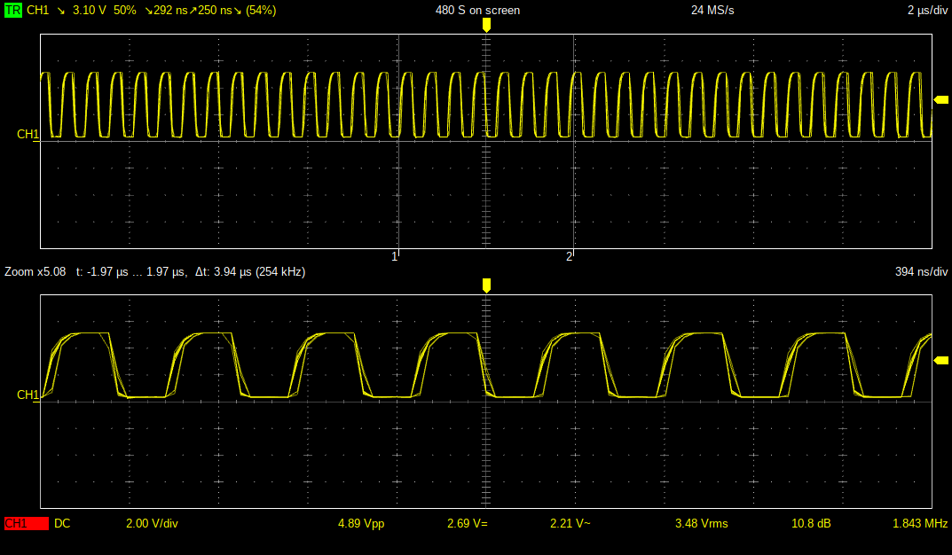
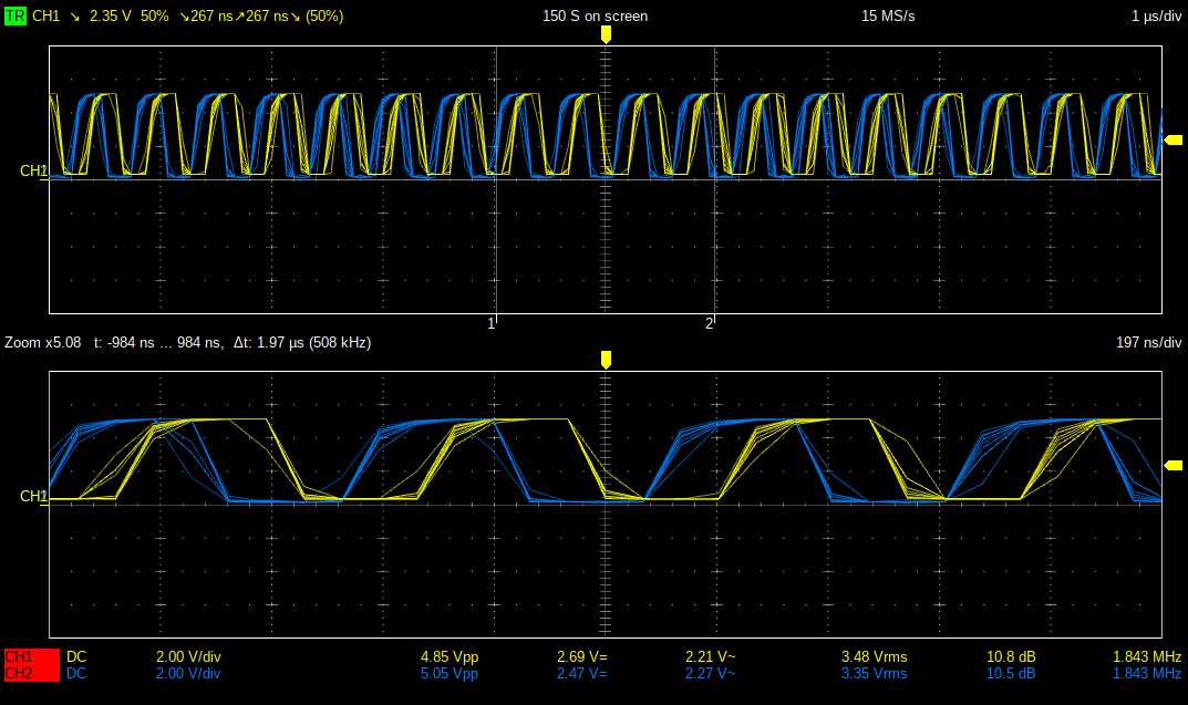
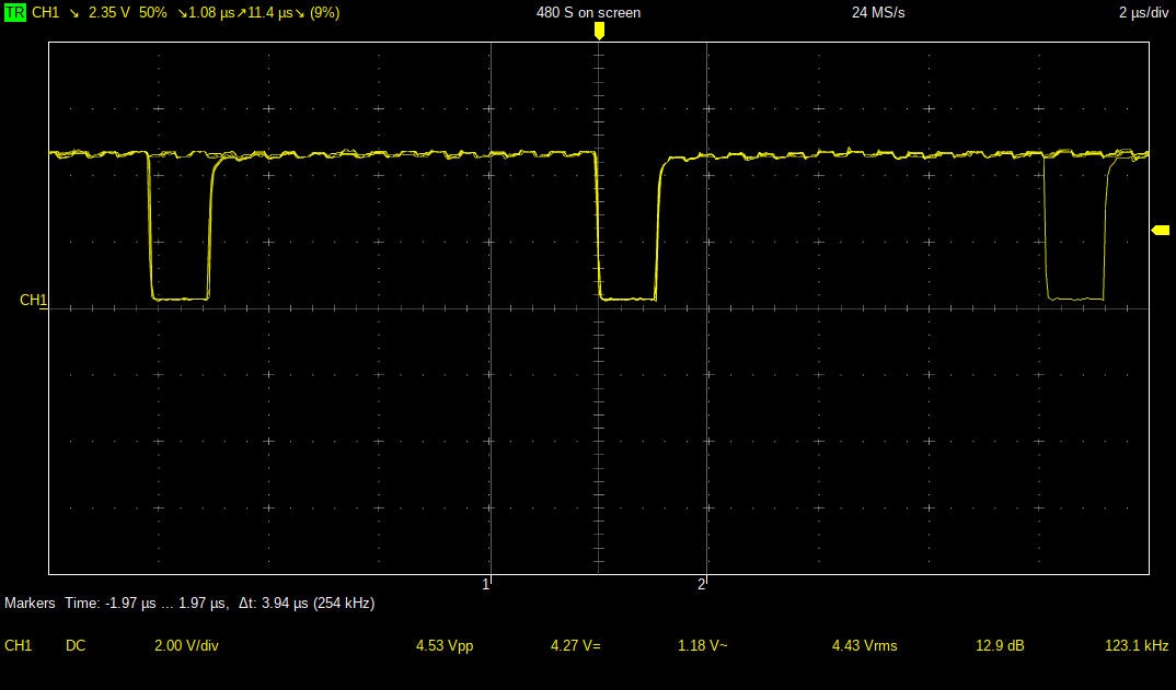
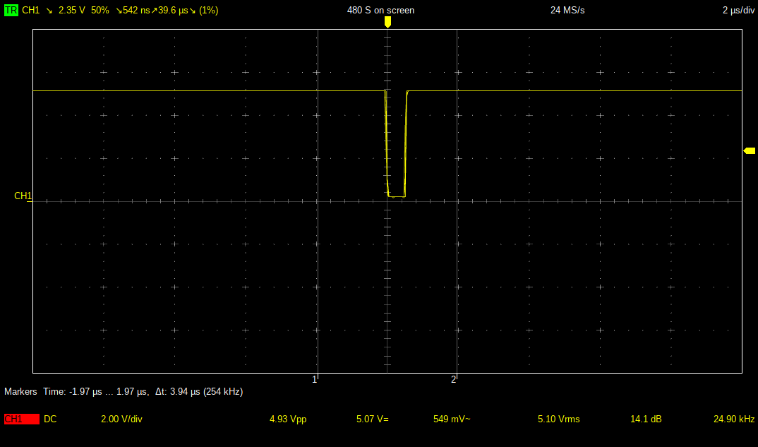
    I have a very minimal scope, so unfortunately these screenshots are not super great but they basically demonstrate everything is fine with the board:

    CLK (Tests the crystal oscillator)

    E (Tests the internal clock frequency):

    E&Q (Tests the internal clock divider / clock generator ): 

    R/W:

     Determine's if the CPU is running through code, This would be constantly high if there was an issue, or the cpu was not sitting at the ASSIST9 ready prompt.

    A000 (Shows the ACIA is being selected every so often for read checks):

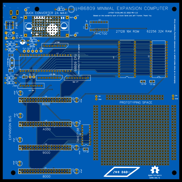
    I spent some time fixing the routing issues with the PCB and adding a probe point for the R//W lines moving some of the packages closer to where they are used and moving the points so they don't introduce unnecessary issues (especially with routeing).  I also brought the individual pull up resistors for the unused signal lines closer to the rest of the termination.  This allowed the RAM and ROM to be routed much easier.  

    As you can see I shrunk the prototype space to include more empty space to route into I put the RAM /ROM selection gates at the top and I moved all of the chip labels off the actual socket footprint to make this easier to read once the chips are installed in the sockets.  The +5V Fill is on the top, with the GND Fill on the bottom.  I Joined the "island" planes in spaces using vias with .6 mm traces (these are double width the same size as the +12V Tracks leading to the switch and the DC-DC converter).  Since the 5v and GND were not double routed, there were places that it needed to be linked up.

    I Tested the Fit on the PCB mounting holes, which was perfect!  Here it is mounted to an open frame Mini-ITX platform.  The mounting rails for the single PCI-E slot in this form factor lines up perfectly with the right angle connector for the card edge being mounted coming out of the back side...

    Read more »

  • False starts are sometimes the best starts....

    Dave Collins08/15/2022 at 18:00 2 comments

    So it has been a long time since the last update, but here goes....

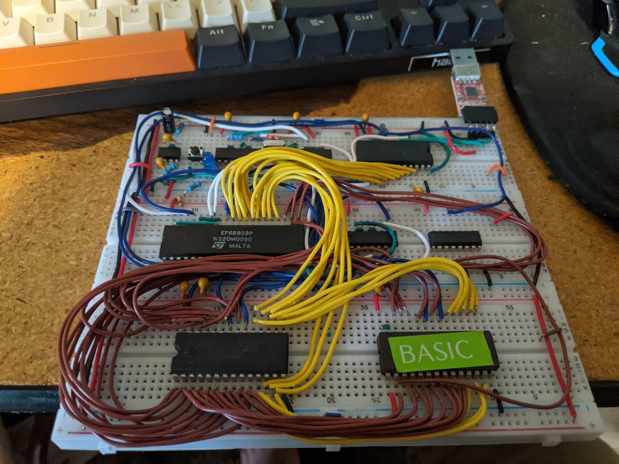
    So I built up the Grant Searle / Jeff Tranter Single board 6809 computer on a breadboard: 

    If you haven't checked out the minimal 6809 on their sites its a good read both of them, and definitely more educational than anything you'll get from me!

    I put together the reset / clock divider we talked about in my last update.   Consequently, a lot of the schematics were poorly  drawn in that update and so it's best to ignore them. It worked like a charm but like so many things I wound up simplifying further and just hooking the crystal up to the CPU directly (its built in to the chip and though I don't think anybody has de-capped a 6809 to check (that I know of?)   It is VERY likely the clock is normalized with an inverter heading into clock generation inside the chip so why bother?    In the end, being able to scale the chip clock was fun to be able to run the CPU at 1 MHz, but I was always going to put the vintage chip in my collection and simply use the early 2000's era Thompson / SGS Version any how; and it runs at 2 MHz.

    Lets take a trip on down to feature creep city:

    It really is the city where good projects go to die...

    I knew about this issue (lets face it no good project is immune).  I had an idea to learn a little bit about address decoding, and expansion busses.   I decided I wanted a few things out of this computer build:

    1. I wanted it to be low cost ( not made of money, retro kits are expensive lets be real somebody has to pay for the time and energy that goes into making these things into kits, documenting them, distributing them etc.) 
      1. This means I wanted to start with a open or very simple design and expand
      2. I wanted to add very few parts, again to keep the costs down.
      3. I wanted to learn about address decode, and busses the way I learn things by doing and making mistakes.
      4. I knew, and accepted it wasn't going to be perfect but I wanted it to at least work; and be smart and minimal so that as many people could try it out or expand on it like I expanded on the last two projects.
    2. I wanted the chip count to be low, and I wanted the chips to mainly be HCT again for cost reasons as well as availability (you can still get through hole HCT chips new, at generally reasonable prices.)
    3. I wanted there to be a PCB, and example expansion card PCB I could release as open hardware.  I didn't feel right taking somebody else's design and hard work, and selling it as a kit to make money off of.  (even if i was modifying it in a big way It still runs Jeff's firmware, witch is kind of grants firmware, Which is KIND OF Microsoft's firmware.)  This is a clone, with bells and whistles and I am lucky to just have the community engagement in kind based off of the work of these two people.
    4. I wanted to focus on the 6809 and pin compatible 6309, I had no plans to directly support the external clock chip versions.

    I set out to build a back plane. I had no idea what a rabbit hole this was going to be.  First off lets be real, The world doesn't need another back plane standard for retro computers: 

    • STEbus
    • Euro card
    • S-100
    • Z50 Bus
    • even RC2014 (don't even get me started!)

    this was a huge mistake. full stop.

    I released several ideas for sub-par backplane designs, similar to RC-2014 and Z50 bus on some of the groups i frequent on Facebook and prepared for worst.  The internet is a great place to get feedback, but its also frustrating for people like me who are learning, and might not get everything right all the time (how dare I right? )   Lets face it, its never any fun to be told that you have a terrible non-starter of an idea.  But to be honest I rather appreciated it ... though it did do a number on my mental space for a few hours, I'll live this is how we learn.

    ... Read more »

  • Here's the plan...

    Dave Collins07/19/2022 at 05:33 3 comments

    Here we go.....

    So I needed a pallet cleanse of my CMOS CPU project that's kind of hit a snag.  I bought this 6809 in a vintage electronics suppler that is about 40 minutes from my house called Chester electric. They are a small electronics suppler and they have everything! Seriously from HAM parts to boards you can buy to pull micro's off of; it is my happy place.  I never manage to take pictures when I'm there but  here is a video Rinoa's Auspicious Travels took of the inside of the place: 

    if you are ever in southeast Wisconsin its a very interesting place to visit, I highly recommend it!  

    The CPU: 

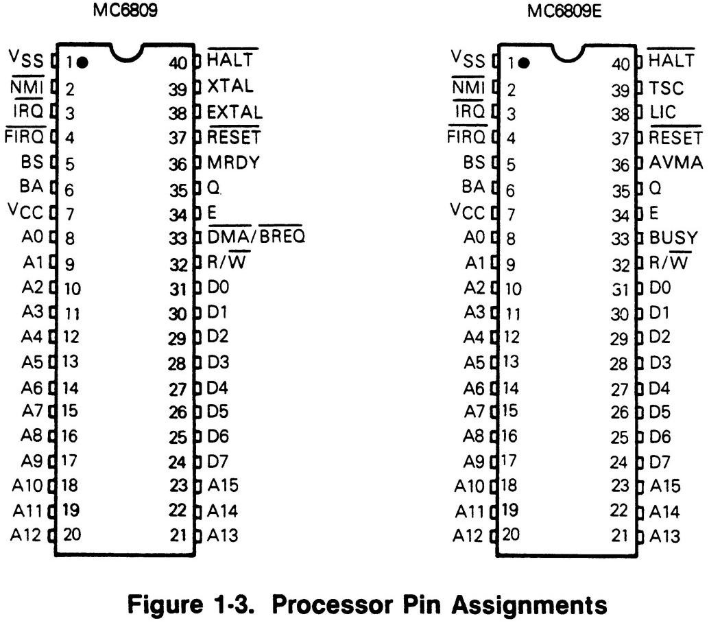
    Its important to talk about the different types of 6809's.  As far as I can tell there are 3 speed grades B, A and standard (68B09, 68A09, and 6809) these versions have a "On chip Clock Circuit".  Additionally, there is a E variety that brings the divided clock outside of the chip.   This computer uses the on chip clock variety.  By way of comparison, the Tandy Color Computer (CoCo) uses the E variety All of these chips end with E[Package Type] and so they would be: 6809E, 68A09E, or 68B09E.  The package type labeling varies but simply put P = plastic or C = Ceramic, and vice versa.  Also, as a word of caution, it is easy to confuse the chips as they are all 40 pin packages but the pin outs are greatly different. There is an adapter available although I've not tried it and have no idea if it works well. Here's a cross reference of the CPU's I shamelessly ripped from google image search from this source:  


    The plan:

    I'd like to build a basic computer (at first, though I'm not limiting myself).   I'll base the initial build off of Grant Searle's 6809 basic computer.  If you've never been over to his website you really should its an invaluable resource.  A while back i built a terrible first attempt PCB of his keyboard and TV interface.... i'll not link it here as it's not  a very good example of the design but if you look hard enough I'm sure you can find it.  

    Grant has spent a lot of time and energy on his website, so if you want schematics for his original build, he's asked everybody to not re-post them so head on over there to take a look.

    To start I would like to improve the clock circuit. Since the chip has an internal crystal oscillator amplifier pin (XTAL), grant simply used it with a crystal and two capacitors. This arrangement is actually specified in the datasheet, however, since there are 3 speed grades of the 6809 (non-E Version) it is nice to have a little divider circuit so that we can use the lowest and highest speed grade with a jumper and 1 crystal.  Since were using an ACIA as a the initial display and user input interface, it is fortunate grant selected a 7.3728 Mhz crystal for his design.  Simply, with that clock frequency we can get a baud rate of 115200 out of the AICA. However, by building a clock that can both supply a perfect clock for the serial interface and also optionally divide itself down to provide something closer to 4 Mhz ( ~3.68 Mhz), we can use the lower speed grade chip without harm.   Additionally the CPU divides down the clock further, by a factor of 4.  So in the end we get approximately 1.8 MHz. for a B speed grade chip and .9 Mhz for a standard 6809 (this sounds slow but compared to chips of the day it's actually right in there).

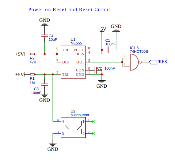
    Since grants design, does not have (or really need for that matter) a power on reset, I had to add one for the clock divider in my clock. And so I went with the standard, substandard, C64 Reset Circuit:  

    For the simple reason I've used it before, and it works.  I may experiment with one of those reset chips, that provides watchdog / brownout protection, but for now this is a very common known design.  Since I had to put in the inverter chip any way...

    Read more »

View all 5 project logs

Enjoy this project?

Share

Discussions

JNP-3R wrote 09/07/2024 at 23:06 point

Thanks so much for the detailed writeup on this, and for turning me on to Jeff Tranter's ROM. I've got another 6809 build based on Grant Searle's design (a boardI bought from eBay without docs) and it's great to have a resource for digging deeper into expansion / modification.

  Are you sure? yes | no

Steve Toner wrote 09/16/2022 at 04:25 point

A couple of thoughts:

1. 74ACT parts will give you more drive capability (and speed) than either HCT or LS.

2. I'm not sure why you're pulling up the address and data lines - U7, U10 and U11 can probably be eliminated.

OK, there's a third:

3. I wouldn't trust that buck converter & would add a crowbar circuit in case it fails in a bad way (passing the input voltage straight through to the output).

  Are you sure? yes | no

Dave Collins wrote 09/16/2022 at 08:28 point

Hct was a parts availability choice (I can get them, they are inexpensive, they Are familiar to me ).   I am pulling up a number of open collector signals as well (which expect a normally high state to run correctly). The data and address bus was to prevent the bus (a bit ) from self biasing considering the unknown state of it due to open expansion connectors. As to if it effectively, does this Better than some other form of bus termination remains to be seen, though I'm open to a better suggestion if you would like to educate me. The buck converter is optional, there's a prototyping space if someone wants to build a better power supply or use a linear voltage regulator or some such it already has reverse voltage suppression, and a diode could easily be run on the backside of the board for over voltage protection. Additionally, there's a good write up here: https://lygte-info.dk/review/Power%20Adjustable%20buck%20converter%20LM2596%20UK.html on the module. Given I'm not overloading the output even over 1A it's not of a major concern to me.   As always, I am not an engineer, and don't claim to be one so I could be completely wrong, so all of this is best taken with a grain of salt.  I will say I did at least have one other person look at the output characteristics of the power module and agree it's " good enough", for what it's being used for here. 

  Are you sure? yes | no

Steve Toner wrote 09/16/2022 at 16:20 point

The buck converter comment was not about overstressing it - it's about failure modes and the questionable nature of the parts used (possibly counterfeit - you don't know).  They can fail in a way that presents the input voltage on the output, which will likely destroy your hard-to-obtain vintage parts.  A crowbar circuit is cheap protection (but not included on the buck converter module), and I don't think I'd use one of those modules without one when using vintage parts...

CuriousMarc did an interesting series of videos on this topic (not related to this specific buck converter module, however) on YouTube a while back: HP 9825 Repair - YouTube

  Are you sure? yes | no

Dave Collins wrote 09/16/2022 at 16:39 point

It makes a lot of sense, I guess I haven't ever had a problem. But I know there's not always going to be parts availability or others would like to use something else, which is why I put a plated through hole space under the footprint for the module so you can If you like build whatever kind of power supply you would like. It's also very simple for me to sneak a transient suppression diode under the supply, I'll order some.   If someone wants a full crowbar circuit there's more than enough space on the back of the board via the prototype space.

  Are you sure? yes | no

Similar Projects

Does this project spark your interest?

Become a member to follow this project and never miss any updates