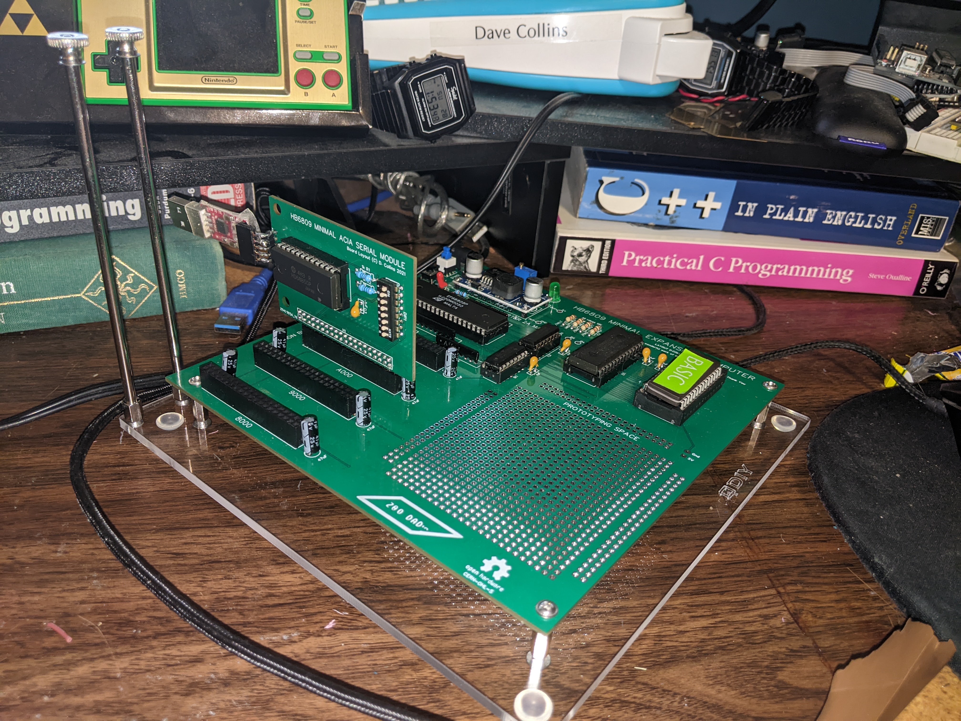
-
Working on Jeff's Combination ROM / W27E257 Tests & CMOC
02/05/2023 at 19:36 • 0 comments![Hel ord Hel ord]()
it's not Hellorld... but so close So it's been a while how about an update?
I have been working towards a number of projects lately including a interesting series (i think) on the ZX81 that I am working on, as well as HBSound my 8 bits sound card similar to the Disney sound source (with a beefed up sample clock circuit). I landed on trying to get CMOC fired up on the HB6809 to a state that I can start writing some faster code (using a c like compiler). The best part of this hobby is that you can really get lost in the minutia of the varied areas of home brew computing. This week was software; and like so many things I really threw myself into it.
Really putting your foot in it:
So if its not obvious, I am an autodidact when it comes to hardware design. I try to test everything and build safe functional circuits that are close to the lower speed designs of the 70's and 80's, but a lot of this is experimentation and keeping a solid notebook of what I think is going on. I believe what Ive built in the HBSound is just about the best design I have ever made. However, what I lacked at the end of the project was a really good way to test the sound card at speed. Enhanced basic is not really fast enough to write the buffer and produce anything further than a 200hz tone, and I am a complete novice when it comes to 6809 assembly (I know just enough to be really dangerous). I am however proficient in C, specifically the flavor or C that was kicking about in the early 90's on 16 and 32 bit CPU's. I also know a fair bit of Pascal, as well as some 8080 assembly language. There exists a c like cross compiler for the 6809, called CMOC, it's very similar to C, and produces .srec files with little issue for quick loading over serial.
I set out to get CMOC, to produce working machine language that Assist09 can load. In an effort to facilitate this I had to figure out how to re-direct a minimal amount of the standard library to support the ACIA at A000. The manual for CMOC actually is fairly comprehensive and includes a section on doing specifically this. Additionally ASSIST09 has a few system calls that allow for things like sending a character and reading from the terminal a snap:
*******************************************
* ASSIST09 MONITOR SWI FUNCTIONS
* THE FOLLOWING EQUATES DEFINE FUNCTIONS PROVIDED
* BY THE ASSIST09 MONITOR VIA THE SWI INSTRUCTION.
******************************************
INCHNP  EQU     0               ; INPUT CHAR IN A REG - NO PARITY
OUTCH   EQU     1               ; OUTPUT CHAR FROM A REG
PDATA1  EQU     2               ; OUTPUT STRING
PDATA   EQU     3               ; OUTPUT CR/LF THEN STRING
OUT2HS  EQU     4               ; OUTPUT TWO HEX AND SPACE
OUT4HS  EQU     5               ; OUTPUT FOUR HEX AND SPACE
PCRLF   EQU     6               ; OUTPUT CR/LF
SPACEF  EQU     7               ; OUTPUT A SPACE
MONITR  EQU     8               ; ENTER ASSIST09 MONITOR
VCTRSW  EQU     9               ; VECTOR EXAMINE/SWITCH
BRKPT   EQU     10              ; USER PROGRAM BREAKPOINT
PAUSE   EQU     11              ; TASK PAUSE FUNCTION
NUMFUN  EQU     11              ; NUMBER OF AVAILABLE FUNCTIONS
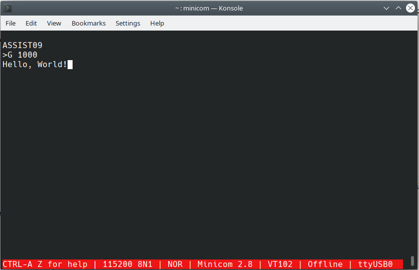
We can call these by simply entering a software interrupt followed by a byte describing the function we'd like to do (very similar to a BDOS/BIOS call in CP/M.) Armed with this knowledge I set out to build a output routine for CMOC that would use some of these routines to see if I could get the terminal to output an obligatory "Hello, World!" program.
The obligatory "Hello, World!" program:
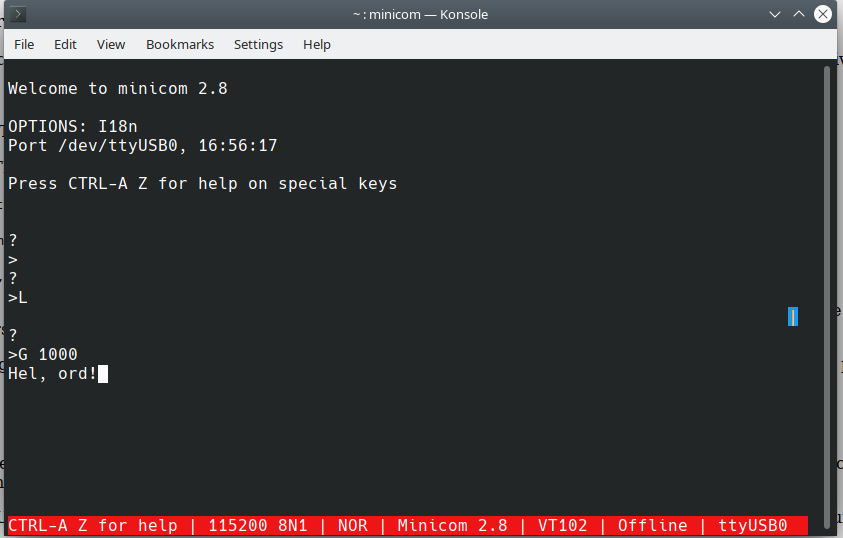
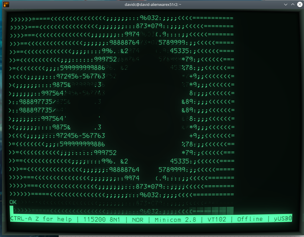
Before I discovered the system calls in assist09 I found you could output characters to the terminal by simply writing to A001, the main issue with this is that this process requires either a programmable interrupt and a buffer to handle waiting for the appropriate time when the ACIA is ready for data to output --- OR a subroutine that scans and waits for the register in the ACIA to show that it is ready (by returning 0x2). If you simply send the character data to the interface you will find it will drop characters (like the picture above in the lead in).
To build a custom output routine is simple in CMOC and they did a lot of the ground work as well as documenting it in the manual. here's what I came up with:
// ASSIST09 SYSTEM CALLS USED
#define OUTCH     1       // sends a character to the terminal
#define MONITR    8       // soft start ASSIST09
void newOutputRoutine(void) {
    char ch;
    asm {
        pshs     x,b     // save regs swi handler uses them
        swi
        fcb     OUTCH    // system call to ASSIST09
        puls    b,x      // put them back
    }
}

// call the monitor to soft start...
void softStart(void) {
    asm {
        swi
        fcb    MONITR    // system call to ASSIST09
    }
}
The soft start routine is not essential but is useful for returning to the monitor from the program termination.
You can then tell CMOC to replace the existing output routine with:
// console redirect --- this is copy paste from CMOC Manual
    setConsoleOutHook(newOutputRoutine);
This needs to be called before you start using things in the standard lib that use the character output routine. But if you run the test program:
![Sucsess! Sucsess!]()
Sucsess! This worked well using the following to make the compiler produce files we can use, the command is simply to tell CMOC to build SREC as the output (this is the s19 file format similar to Intel hex). Then we tell it to use the FLEX as a target. FLEX is a good choice because it has similar output characteristics to the HB6809 (using a ACIA) and we can avoid issues with control codes specifically being mismanaged by the terminal. If you are interested the reason is burred in the standard lib code for CMOC, but following the calls to send a printf we can see that for most of the targets the strings are sent untouched - with exception to the default target the Tandy COCO, and FLEX. COCO takes the <LF> control code (sent by \n in a printf statement) and converts it to a <CR> ... but then when the COCO processes this it produces <CRLF>. FLEX (and the HB6809 expect <CRLF> to make the line advance and the cursor to return. To resolve this issue CMOC is hard coded to make the changes necessary so that when you write :
printf("Hello, World!\n");The cursor will drop to the correct location on the next line in the terminal (or screen buffer in the case of the COCO.) I haven't tried it but I believe the dragon behaves similarly.
TLDR; you compile and send code like this:
cmoc --srec --flex hb6809.c

and then at the assist09 prompt:

>L
 <begin ascii transmission from terminal sending the .srec file>
As the interrupt routines for serial communication are not added to the combo ROM (as of yet ... though this might be a moot point with a fast UART --- more on that later). I still use Jeff's recommended ascii -xfr setup to send files over serial:
ascii-xfr -l 200 -c 10 -s <filename>This tells ascii-xfr to wait 200ms between lines, and 10ms between characters. This transmits the file to the terminal and then when completed assist09 returns 00. You usually have to press enter. After you have loaded the file, then you have to use the 'L' command from assist9 to load the code at the entry point. If you've not specified it the default origin address in FLEX is 0x000 so you can load your program from memory by typing:
G 0 <---- Zero not an O
If everything worked you should be greeted with the output of your program. Additionally I had to use the soft start for the Monitor (call is MONITR)) ~ you can jump to the reset vector in the ROM (which for now is at a fixed point @ 0xF837) but if it moves due to changes your code will need to be updated, using a soft start in the ROM via a system call will manage the monitor location in ROM for you.
ROM Changes:
In looking deeper at the ROM (to try to figure out how the system calls work) I uncovered a curious detail about the RAM allocation for the monitor A snip from the README.md for the combination ROM:
This is a variant of firmware that combines both Microsoft BASIC and
the ASSIST09 monitor into one ROM. It also includes my disassembler
which adds a new monitor U command and trace function which adds a new
monitor T command.

It comes up in ASSIST09. You can start BASIC by running "G C000".

Memory map (16K EPROM):

BASIC         $C000 - $E3FF (9K)
DISASSEMBLER  $E400 - $EFFF (3K)
TRACE         $F000 - $F8FF (2K)
ASSIST09      $F800 - $FFFF (2K)

RAM usage:

BASIC         $0000 - $0178
DISASSEMBLER  $6FD0 - $6FDC
TRACE         $6FE0 - $6FFC
ASSIST09      $7000 - $7051
If you consider the space between 0-7000 as fair game for coding you are left with 28672 bytes of space. I asked Jeff if he thought there was any reason that moving the allocations up the map to the top of the ram would be an issue, and he stated he didn't think it would be a problem. I did a little more digging and determined that ASSIST09 uses approximately 81 bytes for variables in ram to operate (which we need to load and save programs and for the system calls.) Additionally, the monitor racks this 81 bytes under the system page which is another 255 bytes. this means we can start the ram space for the monitor at 0x7EAB (giving ourselves about 4 bytes of wiggle room to the end of the RAM encase the need for revisions arise.) This new location leaves us with 32427 bytes of ram between the bottom of the monitor reserved area and system page, and the bottom of ram. If you'd like to not write over the trace program and disassembler's ram area its a bit tighter (at 32387). The Basic stack and variable space also uses approx 376 bytes of memory at the bottom of the ram, which for reasons I'll explain shortly I'd like to not touch. Bringing the total available space to the programmer after revisions to 32051 bytes of continuous memory that can be played with without breaking ASSIST09 or basic.
I also did the math to relocate the work areas for the disassembler and the trace functions of the ROM what I came up with is the following:
BASIC         $0000 - $0178
DISASSEMBLER  $7E2A - $7E36
TRACE         $7E3A - $7E56
ASSIST09      $7EAB - $7F00 -- (below the 255 byte system page)

ASSIST09 requires an offset -7955 below its ROM location which is
coded to line 8485 of the monitor source under variable RAMOFS.

The other two added functions are ORG statements at the beginning
segments.

Note: there is approximately a 4 byte pad between sections, this
seemed smart and as Jeff had already done this it was easier to
do the math for the calculated area moves.
I will add the resulting changes to the github, along with a .hex file for both 16k and 32k ROMs if you would like to play with it.
Testing the design with a Winbond W27E257 and creating a new ROM image:
The 90's gave us a lot of neat / weird things, one of those things are the W27E257. The W27E257 is a pin correct replacement for the Intel D27256 optical erasable EPROM, but using EEPROM technology. Since its getting harder to find replacement the D27128 and typically you can use a D27256 as a direct replacement, as long as the top address line A14 found on pin27 is managed properly in the design. In the schematics for the HB6809 pin 27 is tied high, and we can use the D27256, as a drop in replacement if we start the code for the ROM at 0x4000. Since this is true, this also means the W27E257 is a valid part to swap in place. Having a electrical erasable EPROM has a ton of benefits, the most beneficial of which is the ability to erase and write it electrically. Additionally since these chips were used in LOADS of 386, 486 and Pentiums, its very easy to get these ROM chips off resellers for around 2 dollars from the usual sources electronics recycling companies use (ie. EBAY). It is as simple as burning the ROM code to the EEPROM starting at 0x4000. I've provided hex files that correspond to the correct offset, but if you are creating a new ROM from source. You need to set the file start address C000, and the buffer start address 4000.
Compiling a new ROM from scratch is essentially using a specific version of as9:
as9 <assist09.asm> -l c s bin s19 cre nowThe resulting compilation will yell about the comments in the assembly file, this is fairly normal and has to do with the age of the assembler. they can be safely ignored.
Converting the ROM code to a intel .HEX file, is recommended as buring the .bin to a rom appears to be fairly broken at least with the TL866 II. The best way to do this is with srecord the best directions for it's use / installation are here but just encase you are merely interested in the command:
srec_cat <input.srec> -Motorola -o <output.hex> -IntelThe resulting .hex file will start at 0000, but you will need to set the eeprom burner to read start address as C000, and if using a 32k EEPROM (or a actual D27256) you will need to set the buffer offset to 4000. ie C000 will need to be at the begining of the readable rom space when the rom is selected as it's address decode starts the beginning of the readable area of the rom at C000 in the decode space.
What's next:
I have to finish writing up a test program for HBSound for starts, now that I have suitable tool chain for writing some faster code this seems like the next best thing. I ordered parts for my upcoming terminal project which I will work on next. I also designed an adapter board, for expanding the rom space into the top expansion address range. PCBWay has again offered to sponsor the prototyping for the EEPROM PCB's I expect these to come in the next few days perhaps by weeks end. This will allow me to play around with expanding the combo rom to include SLOAD and SSAVE (*commands for saving and loading .srec over serial via basic *) as well as dropping to the monitor from basic. Additionally I would like the rom to load straight into basic. The advantage to this is then I can try to coax CMOC into using the floating point instructions from within enhanced basic just as they are for the COCO target. This is all down the road from here but I am glad you joined me for the ride thus far. If you are new to my projects thank you for taking the time to check out my mad hobby.
-
Final Build PCB V2.2
09/14/2022 at 05:11 • 3 commentsUPDATE: Thanks to an insightful comment by Doug Merrett You CAN relocate the board ID on boards produced by JCLPCB using the following directions.
![]()
Its finally here!
As of today, I am considering the main build complete. There's still quite a bit of work to do in making some fun optional modules for the computer, but I am comfortable releasing the build files to the general public for anybody to try out. It has been a ride for certain! I wanted this to be a fast, no-nonsense project. here we are roughly 2 months out start to finish. I can't even believe it myself, back in July I didn't think I'd get this far by now but it's basically a complete project. If anything, this really has been the pallet cleanse I needed after coming off such a complex build that, in the end there wasn't much in the way of results. What a relief to finally be here.
Final Road blocks and hurdles cleared:
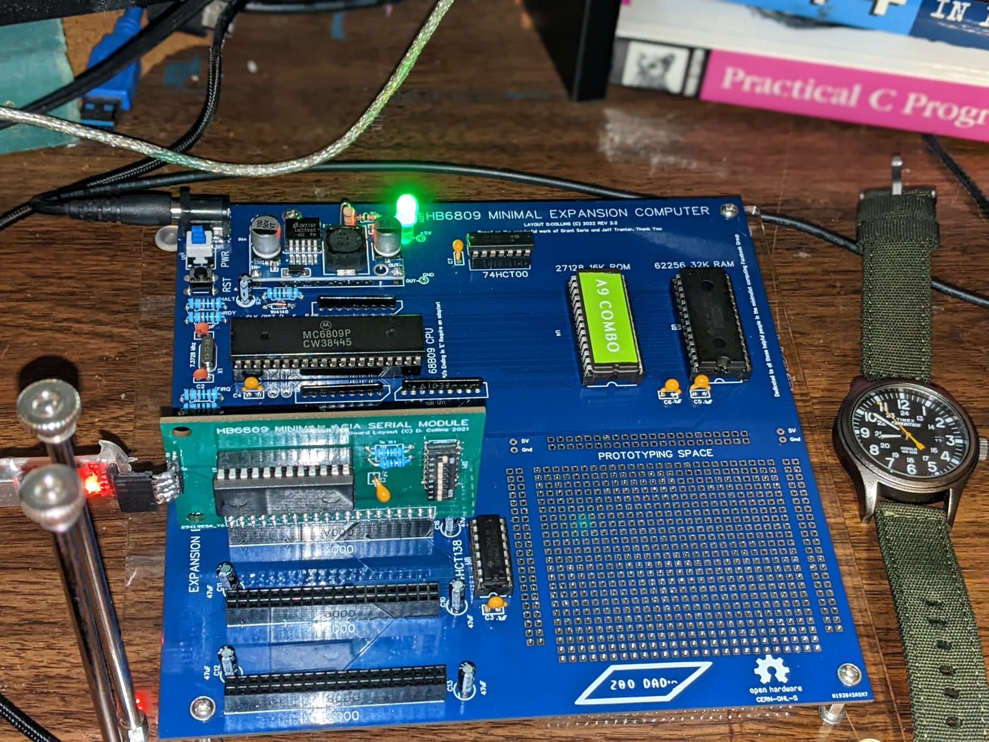
if you've been following the build on Facebook, then you'll know I made a slight mistake during final assembly, resulting in some parts being damaged. If you compare the two boards assembled in pictures then you will see that I have a bog standard Motorola (45 week of 1984) 6809, instead of the proper speed grade 68B09, which the board calls for. I've since ordered the right CPU's from a recycler in Texas and they should arrive soon. The issue came in when I was getting ready to test the lines with the scope, I forgot that I had the board powered on, and when I went to solder the lug to the ground pin on the power supply module, something happened (I still don't know what, but I'm in process of doing some testing to determine exactly what). As soon as the soldering iron tip hit the pin on the module the voltage on the 5V line spiked the LED got very bright and I managed to fry out my circa early 2000's 6809 chip, a vintage eprom, and a hand full of TI 74HCT chips. I suspect that it may have to do with my soldering Iron not being isolated properly but also could be simply that the module is not designed to be soldered to while its in operation, the end result was I had to burn a new EPROM and switch out the CPU for the other one in my collection. It's running happily clocked twice it's rating; I won't run it this way for long but I wanted to make sure the final boards were working before releasing to the public.
![]()
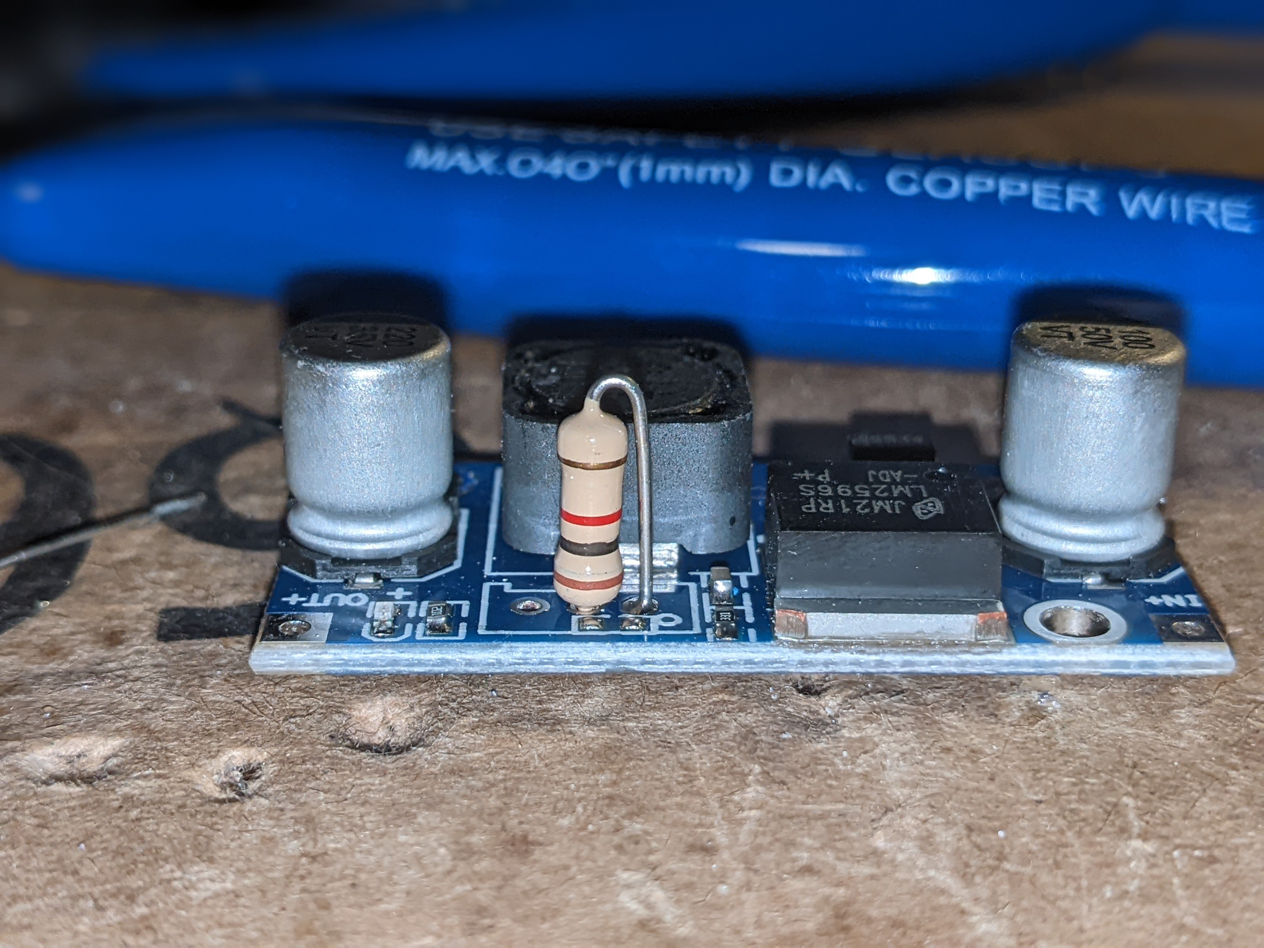
I made a small change to the DC-DC converter module, I removed the high turn potentiometer and replaced with a standard 1/2 watt, 5% 1K ohm resistor. This provides a steady 5v output, without the worry of the pot becoming scratchy, getting bumped or turned. It's absolutely optional but since it was a very easy mod to make I did it because it's some piece of mind really. If you look closely you can see there's a SMD pad which essentially routes to the same location as the through hole pads, so that you can use a simple SMD resistor (it absolutely doesn't have to be 1/2 watt tolerant, this is just what I had on hand ).
V2.2 of the PCB - PCBWay / JCLPCB PCB Comparison:
I will start out by saying, I am looking at these boards like a hobbyist would. I'm not a quality control engineer, so I can only write what I see but the question does get asked, Is the higher price of PCBWay from start to finish for a plated through hole HASL 2 layer board worth it? I think the short answer is yes, but let me spell out a few of my observations so you can get an Idea of what I am seeing. I should also point out, PCBWay, our build sponsor has covered the cost to fabricate the final test boards, However they aren't reviewing my thoughts or requiring me to say anything in particular in my review, what follows is simply my honest opinion on what I see between the two boards.
Finish (Solder mask):
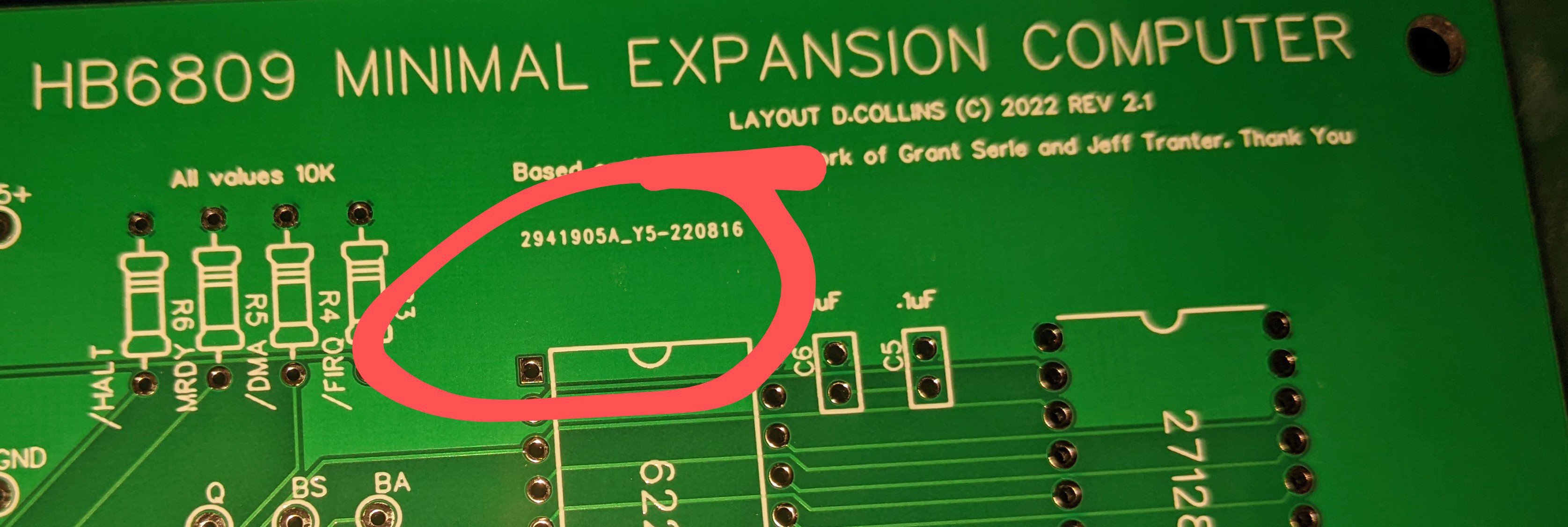
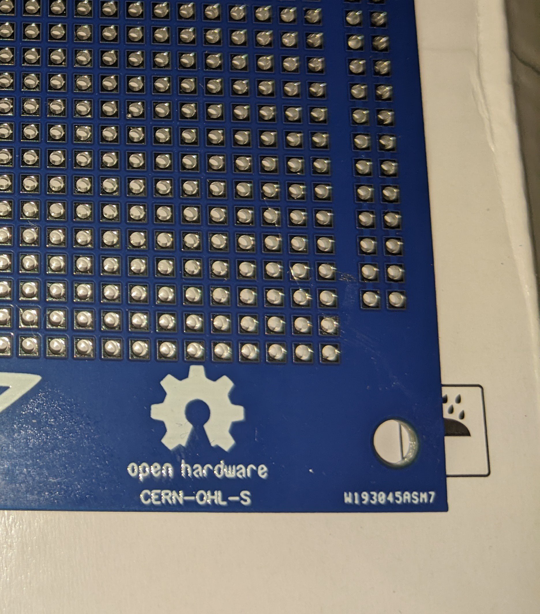
JCL's solder mask comes off exactly like what you would expect from a rapid turn prototype, it is very blotchy in places and doesn't look like a finished product should (although its important to remember its not, its a prototype). Additionally they charge extra for changing the color, and it looks like they go out of their way to put the order number in a prominent location on the PCB. Which is kind of frustrating if your particular about those things. See the update notes preceding this entry for a solution to this
![]()
The boards from PCBWay had considerably more uniform solder mask. Results are very high quality and do not look cheep. Additionally they allow you to select from a few different colors at no extra cost, and even though they are prototypes, they come off as being almost a finished product that you could put into a box as a kit and send to a customer. If they spend as much care and attention on the more higher end finishes than they do on HASL its easy to see the cost is explained by just to this level of care and detail simply spent on the one thing that is plane and visible when you pick up the board, the solder mask. As you can see they put the order number in a discrete location on the board -- as removing this order number is a value added service (just a few dollars) it almost seems like JCL went out of there way to put it in a location that would be a nuisance, as were PCBway simply put it in the lower corner, which has been my usual experience with them.
![]()
Milling and edge finishing:
The milling was spot on by both manufacturers, the plating was only applied to the through holes in locations were they were required, the vias were perfectly installed and I found no issues with either of the boards (save the one design mistake I made on the 2.1 prototype, which is hardly the fault of the manufacturer.) The edge finishing on the other hand was how the boards differ. There was a distinct softness, and minute rounding of the finished boards from JCLPCB. This led me to think that the edges were cut in such a way that they would need to be manually finished to remove sharpness left by either cutting the boards to quickly or with a manual circular saw; instead of routing them in place with a bit sharp enough to bring the edge to the specification, without making it overly sharp. The PCB's from PCBWay on the other hand were cut exactly 170 mm x 170 mm, there was a very firm right angle but the edge was not sharper than one would expect on something that only gets minimal situational handling. My only concern here is that the PCB edge tolerances could be slightly off as a result of softening the edges by a mil or two; and this could result in a PCB not fitting into a custom cut housing if tolerances are very tight the board may be loose in that situation. This is absolutely a rare situation, but if ordering PCB's from JCLPCB this has to be a consideration.
HASL finish:
Both boards had perfectly done HASIL finishing on them. Its hard to be critical on something as basic as the low cost finish done to prototype PCB's. I did try to do some minimal rework in course of soldering components and everything held up well on both boards.
Reflections:
I think the higher cost of the PCB's from PCBWay is more than justified if you have a finished product you'd like to get some boards made for, or for low volume kit fabrication its nice to know that what you are sending out the door is going to be a finished product, that looks like one, Even if the buyer didn't select the highest end finishes. JCL's PCBs while functional would not be good for this purpose, however they are more than sufficient for a run volume of one, or two boards when you are simply trying to verify if a design works, and I think that is there niche.
What is next:
The next course of action is to get a few modules built. I have all the parts on hand to make a resonablly useful sound module, but I'd like to integrate it into the same module as a VIA so that I can use the built in timers, as well as the added IO for a NES/SNES style input. Additionally, I'd like to make a priority interrupt controller, as well as a keyboard interface; for this i will likely use a 8051 micro controller, since it's practically purpose built for doing these tasks. Another thing that I am kicking around is an enhanced serial controller (like the Zilog SIO2) I would like to have hardware flow control for the serial adapter and the ACIA is really not well suited for interfacing with today's modern PC's. Lastly In the back of my head I want to make some sort of VGA interface, I'd like to make something that has input and output registers and manages the video ram internally (sort of like a modern video card), Im toying around with adding a optional header mod to the prototyping space behind the case exposed lowest expansion slot in order to provide DMA signals to just that location for enhanced graphics memory to memory copying.
Conclusion:
What an absolute journey this has been! I have to say thinks again to everybody who helped make the HB6809 a reality! The folks over at the Minimalist Computing group on Facebook, have been absolutely invaluable to everything I've done here. And of course not to mention PCBWay stepping in to bring everything across the finish line! What a wild ride this has been. I've put the links to the build files, on the GitHub up in the summery so that everybody can try out, and check out the boards. Thanks again for taking the time to check out my project!
-
Prototype Layout 2.1
08/28/2022 at 20:24 • 0 commentsUpdate: PCBWay has kindly offered to sponsor the cost of the next run of boards! This is amazing, as I was planning on doing a comparison between JLC and PCBWay in my next post. Follow this space for more soon!
The boards:
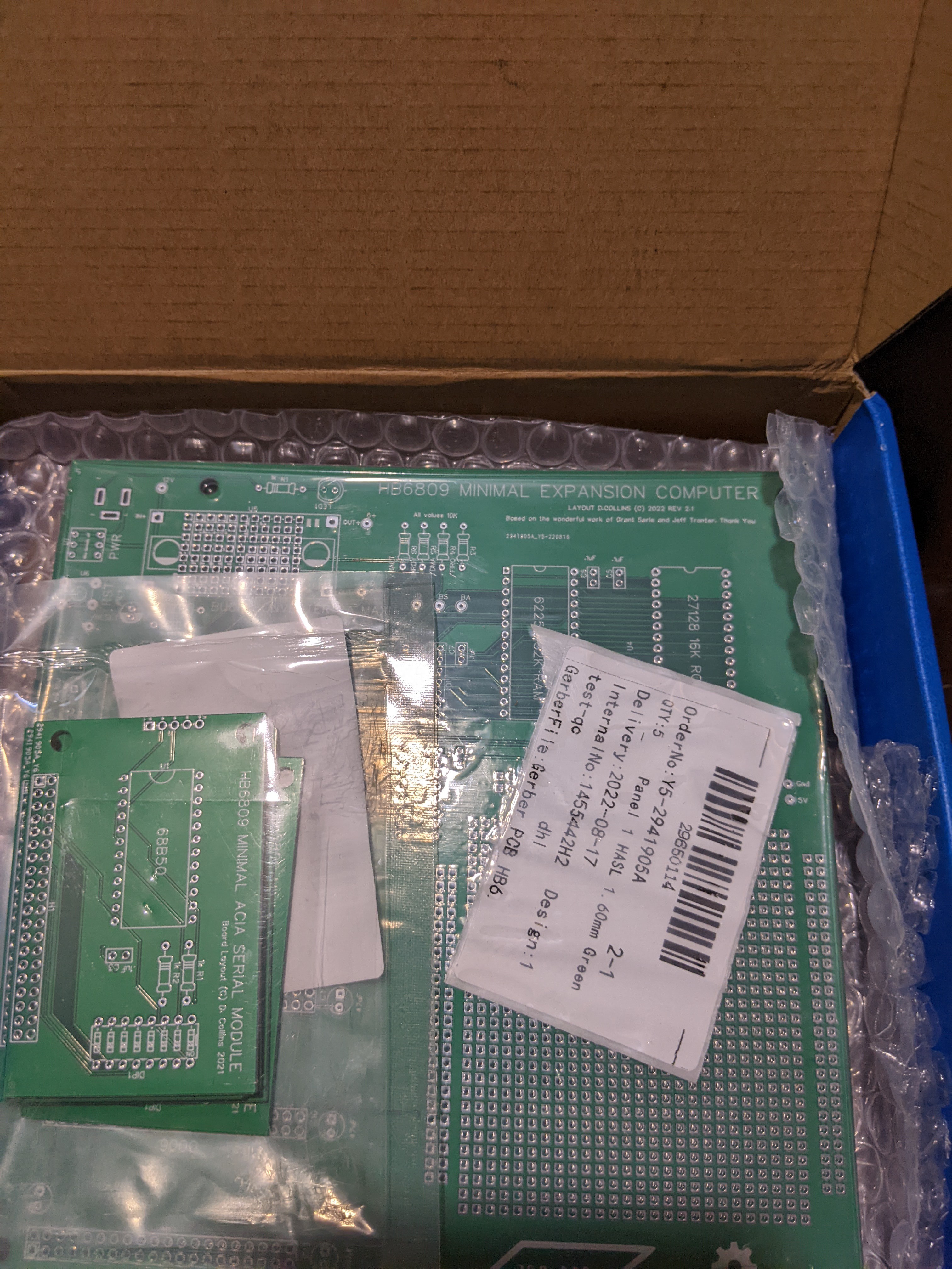
The Boards Were received when the manufacturer stated they would be here. Both the AICA board and the main PCB were packaged with care, there was minor shipping damage to the box but the goods came unhindered inside the packaging. This shipping damage was just slight box crumpling, that could be more blamed on the shipper DHL, than anyone but to be honest I've received things from amazon in far worse shape.
![]()
Fixing the Issues:
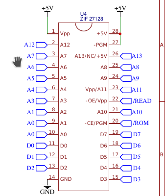
After buildup, the main PCB had some issues. The first big problem I ran into was the addressing on the schematics (which in turn translated to the layout) for the EPROM:
![]()
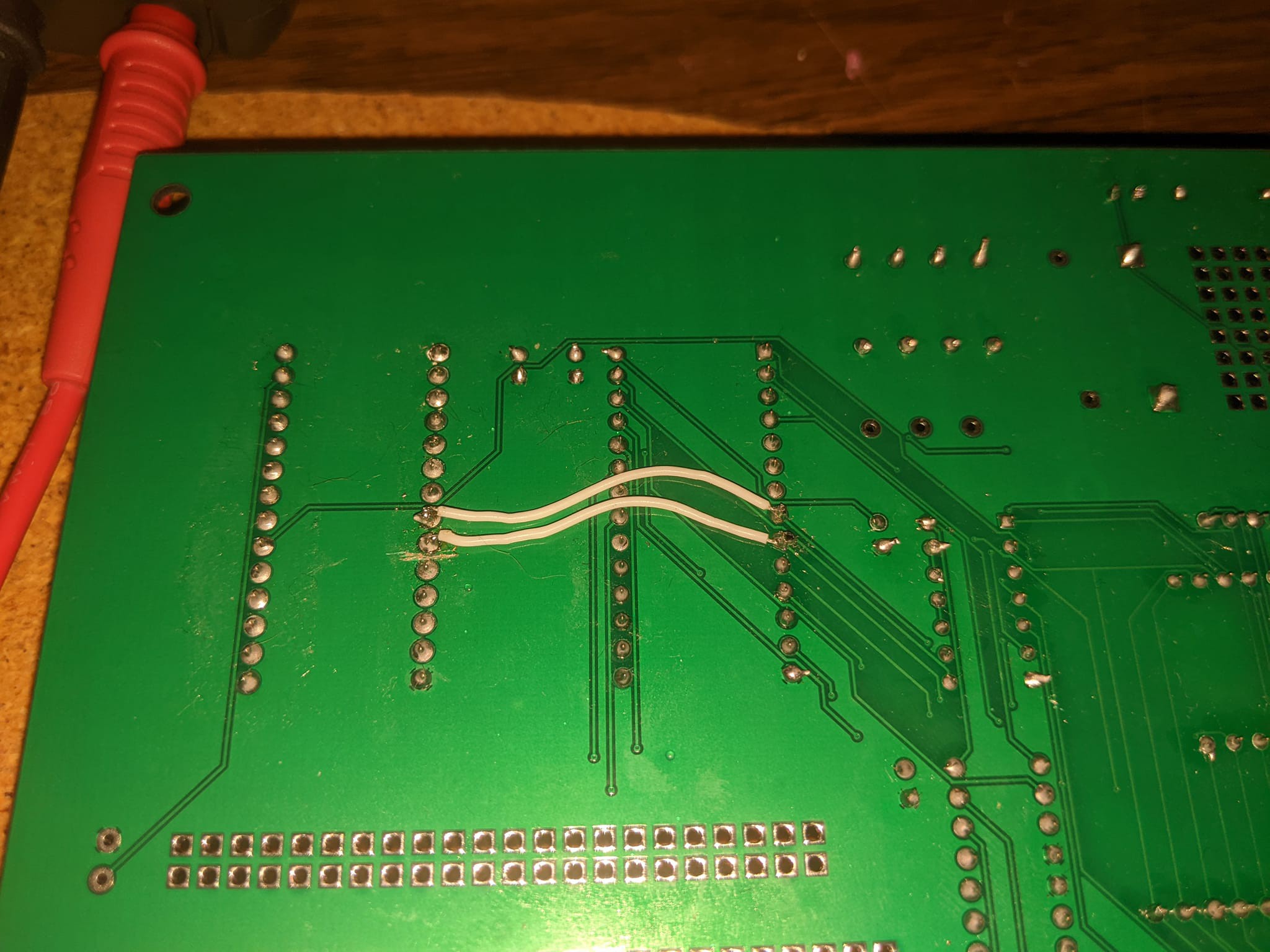
As you can see the A0-2 have potential issues. When i probed the R//W line coming from the CPU with the scope looking for issues I determined that it was basically at it's high state, essentially just reading and probing through the address lines. Upon checking the decode logic I found this to be the case as the selector would simply run through the selected lines over and over again. Fortunately, this wasn't hard to fix, I simply cut the two traces (one between pins 10 and 9, and the trace going A1 on the ram running from pin 8.) Then after that was done I bodged the two pins with silicone jacketed flexible patch wire.
![]()
After doing this I got much more normal r//w readings with every so often it switching between the two signals as it processed through the loop for the machine language monitor. The other issues were a handful of silly auto-router related mistakes such as a few lines running through a plated through hole section and the +5V and GND nets being routed throughout the project because when I went to finish up the remaining routing with the auto router I forgot to select them to skip the routing.
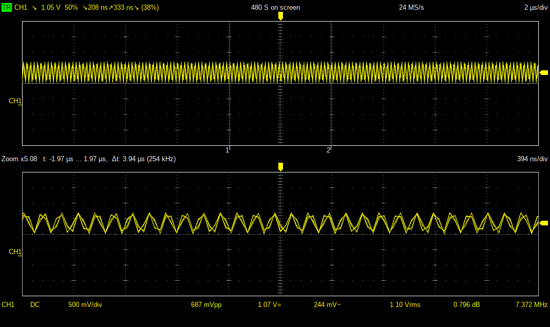
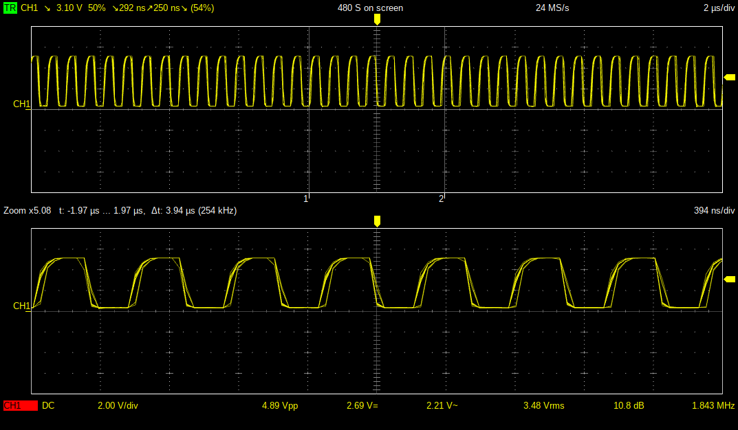
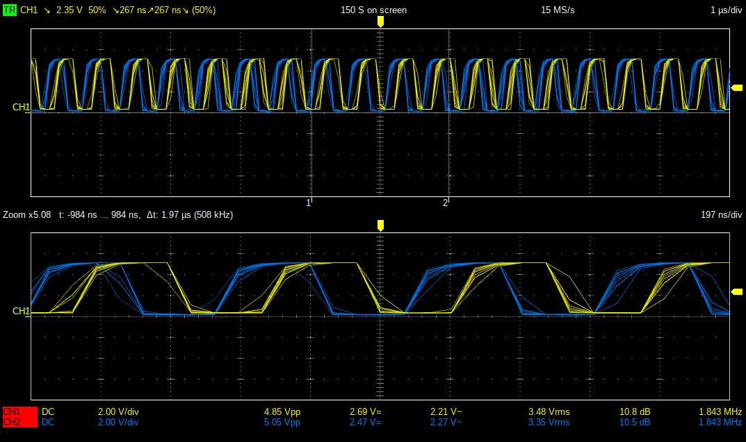
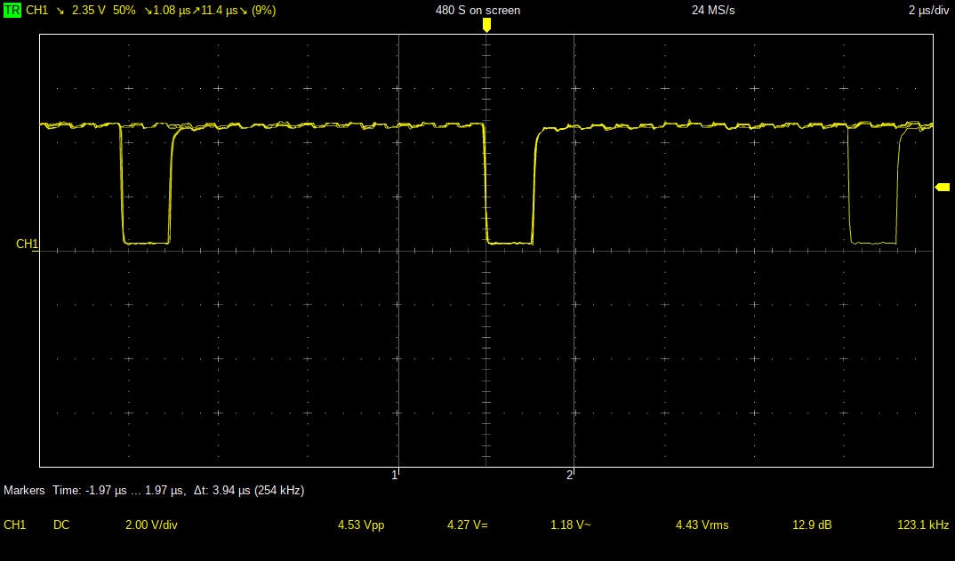
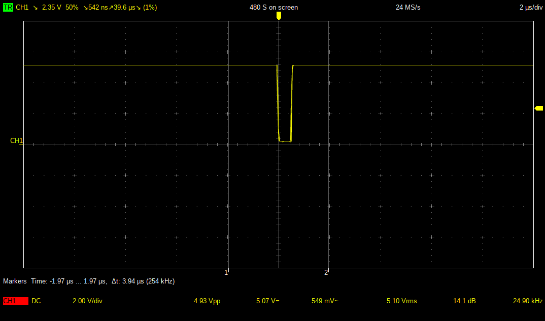
I have a very minimal scope, so unfortunately these screenshots are not super great but they basically demonstrate everything is fine with the board:
CLK (Tests the crystal oscillator)
![]()
E (Tests the internal clock frequency):
![]()
E&Q (Tests the internal clock divider / clock generator ):
![]()
R/W:
Determine's if the CPU is running through code, This would be constantly high if there was an issue, or the cpu was not sitting at the ASSIST9 ready prompt.
![]()
A000 (Shows the ACIA is being selected every so often for read checks):
![]()
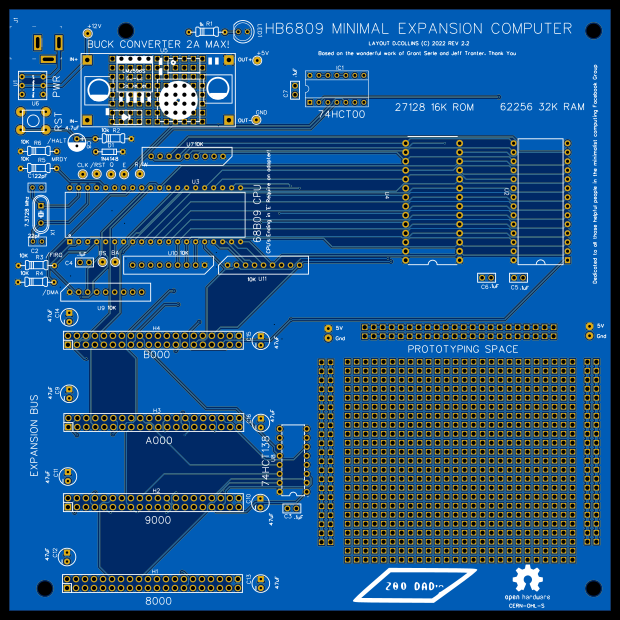
I spent some time fixing the routing issues with the PCB and adding a probe point for the R//W lines moving some of the packages closer to where they are used and moving the points so they don't introduce unnecessary issues (especially with routeing). I also brought the individual pull up resistors for the unused signal lines closer to the rest of the termination. This allowed the RAM and ROM to be routed much easier.
![]()
As you can see I shrunk the prototype space to include more empty space to route into I put the RAM /ROM selection gates at the top and I moved all of the chip labels off the actual socket footprint to make this easier to read once the chips are installed in the sockets. The +5V Fill is on the top, with the GND Fill on the bottom. I Joined the "island" planes in spaces using vias with .6 mm traces (these are double width the same size as the +12V Tracks leading to the switch and the DC-DC converter). Since the 5v and GND were not double routed, there were places that it needed to be linked up.
I Tested the Fit on the PCB mounting holes, which was perfect! Here it is mounted to an open frame Mini-ITX platform. The mounting rails for the single PCI-E slot in this form factor lines up perfectly with the right angle connector for the card edge being mounted coming out of the back side of the PCB. So when I get around to making a display adapter the card should fit into the rails with a 3d Printed mounting bracket, the ports on the edge of the card should fall well in between the rails.
![]()
What's next:
I am getting ready to send off the revisions to have a final run of the main PCB. The Serial card works perfectly, and won't actually need any further work. This time i'll be using a different PCB manufacturer PCBWay, so that I can compare the build quality. I have always been really impressed with the Asian market rapid turn PCB manufacturers, so I am not overly concerned but I like writing about these things as much as I like working on them, so it should be a good experience!
After I verify the PCB's are working, I'll consider this stage of the project more or less completed. Once I know they wok for me I'll release the Gerber files for anybody to try out, and most likely sell any extra boards to anybody who wants them for the cost of shipping (I don't need 10 blank boards just hanging around). I have several plans for expansion modules - a video adapter, a sound card, and a Zilog SIO serial board with a RS-232 port (as well as TTL hook ups!).
Thank you for taking the time to read about this project thus far. I really do hope to soon be able to share the project files, including the easyEDA files, so that if somebody wants to further play around with this design they may.
-
False starts are sometimes the best starts....
08/15/2022 at 18:00 • 2 commentsSo it has been a long time since the last update, but here goes....
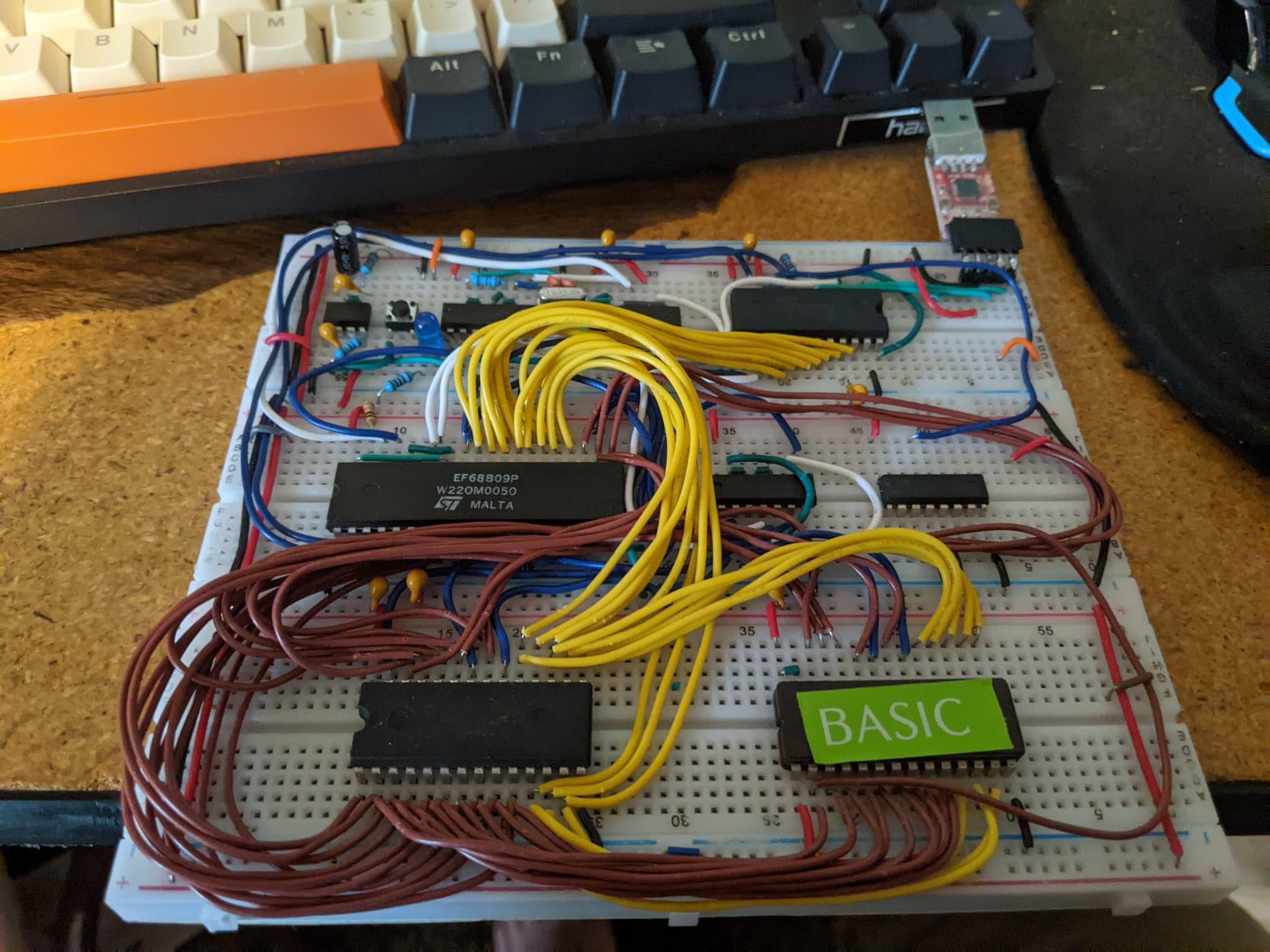
So I built up the Grant Searle / Jeff Tranter Single board 6809 computer on a breadboard:
![]()
If you haven't checked out the minimal 6809 on their sites its a good read both of them, and definitely more educational than anything you'll get from me!
I put together the reset / clock divider we talked about in my last update. Consequently, a lot of the schematics were poorly drawn in that update and so it's best to ignore them. It worked like a charm but like so many things I wound up simplifying further and just hooking the crystal up to the CPU directly (its built in to the chip and though I don't think anybody has de-capped a 6809 to check (that I know of?) It is VERY likely the clock is normalized with an inverter heading into clock generation inside the chip so why bother? In the end, being able to scale the chip clock was fun to be able to run the CPU at 1 MHz, but I was always going to put the vintage chip in my collection and simply use the early 2000's era Thompson / SGS Version any how; and it runs at 2 MHz.
Lets take a trip on down to feature creep city:
It really is the city where good projects go to die...
I knew about this issue (lets face it no good project is immune). I had an idea to learn a little bit about address decoding, and expansion busses. I decided I wanted a few things out of this computer build:
- I wanted it to be low cost ( not made of money, retro kits are expensive lets be real somebody has to pay for the time and energy that goes into making these things into kits, documenting them, distributing them etc.)
- This means I wanted to start with a open or very simple design and expand
- I wanted to add very few parts, again to keep the costs down.
- I wanted to learn about address decode, and busses the way I learn things by doing and making mistakes.
- I knew, and accepted it wasn't going to be perfect but I wanted it to at least work; and be smart and minimal so that as many people could try it out or expand on it like I expanded on the last two projects.
- I wanted the chip count to be low, and I wanted the chips to mainly be HCT again for cost reasons as well as availability (you can still get through hole HCT chips new, at generally reasonable prices.)
- I wanted there to be a PCB, and example expansion card PCB I could release as open hardware. I didn't feel right taking somebody else's design and hard work, and selling it as a kit to make money off of. (even if i was modifying it in a big way It still runs Jeff's firmware, witch is kind of grants firmware, Which is KIND OF Microsoft's firmware.) This is a clone, with bells and whistles and I am lucky to just have the community engagement in kind based off of the work of these two people.
- I wanted to focus on the 6809 and pin compatible 6309, I had no plans to directly support the external clock chip versions.
I set out to build a back plane. I had no idea what a rabbit hole this was going to be. First off lets be real, The world doesn't need another back plane standard for retro computers:
- STEbus
- Euro card
- S-100
- Z50 Bus
- even RC2014 (don't even get me started!)
this was a huge mistake. full stop.
I released several ideas for sub-par backplane designs, similar to RC-2014 and Z50 bus on some of the groups i frequent on Facebook and prepared for worst. The internet is a great place to get feedback, but its also frustrating for people like me who are learning, and might not get everything right all the time (how dare I right? ) Lets face it, its never any fun to be told that you have a terrible non-starter of an idea. But to be honest I rather appreciated it ... though it did do a number on my mental space for a few hours, I'll live this is how we learn.
I devised that I wasn't being true to my design goals. I let feedback drive the features (and thus the complexity to an astounding level.) by the time it was done I was supporting, or trying to support both clock types of the 6x09 family, all of the signals in the CPU and to be honest that was a HUGE Mistake.
Once I had time to think it over, I went with a more conservative design:
![]()
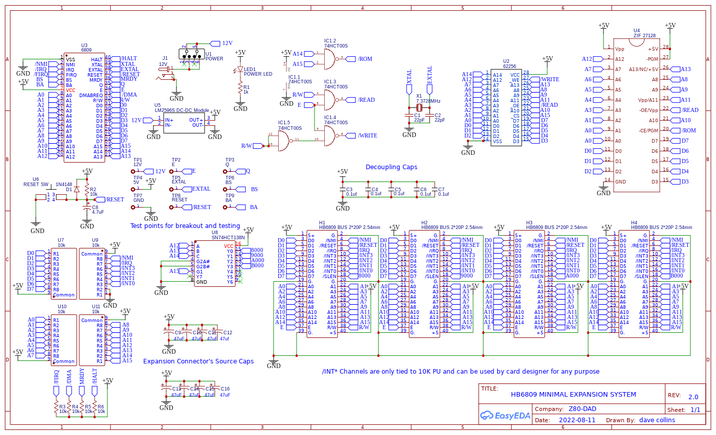
The expansion connector looks like this:
![]()
As you can see this is not a full signal expansion bus, this is simply the address bus, the data bus, the main interrupt, the E clock the R/W signal, a select line (/SLEN), and 4 interrupt channels that only interconnect the 4 slots. The more signals you add the more complex and demanding your connector design has to be. This is truly a minimal what you see is what you get expansion port. I'd not go so far as to say it's an expansion bus, but it has bus like tendencies. If it helps, think of it as a C64 expansion port, except there are 3 of them and they are addressed. The over all expectation is that this will work (or should work) at 2 MHz no problem... I don't know if it will worked with an overclocked 6309 at 5 Mhz with a 20 Mhz starting clock, this would require much more attention to ringing in the signal lines than what I've done here... but obviously its wrong not to try right?
I used a standard (substandard?) 2x20 pin connector. The main board side is female, the card edge is right angle male. As you can see, an idea from comments in one of my posts I laid out the power and grounds so it is impossible to plug the card in and reverse power and ground (the result won't work but at worse it will mess up the address, and data bus lines).
The 4 interrupt channels are for if I decide to build a priority interrupt controller, they are tied high at the bus termination and they go between the cards so that you can pass off interrupts to the other slots to be maintained by a separate interrupt controller. Since they are handy, you could use one of them by simply bodging the broken out test points from the un-routed CPU signals if needed or use it for some other operation between the cards, so long as it is a normal TTL signal it should work.
The changes I did make:
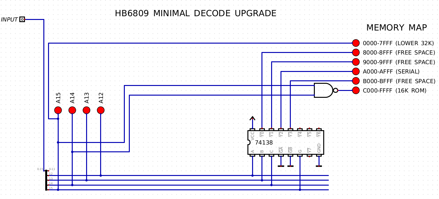
I expanded the memory map slightly, added address decoding to expand the memory map to four 4k blocks, instead of 2 blocks which were minimally addressed. To keep things as simple as possible, and to further simplify the expansions, the address decoding is locked to the slots.
Grant's / Jeff's Memory map are as follows:
0000-7FFF -- 32K RAM
8000-9FFF -- FREE ADDRESS SPACE
A000-BFFF -- ACIA (minimally decoded)
C000-FFFF -- ROM SPACE
The HB6809 memory map:
0000-7FFF -- 32K RAM
8000-8FFF -- 4k free space
9000-9FFF -- 4k free space
A000-AFFF -- 4k free space (ACIA for Jeff/Grants Firmware to work unmodified)
B000-BFFF -- 4k free space
C000-FFFF -- 16K ROM
This is done by simply adding a 74HCT138 to decode the top four address lines in this manor:
![]()
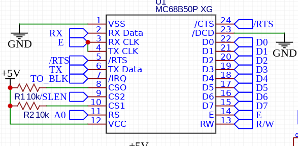
as you can see, the NAND gate is already in place from the previous designs, so this upgrade is fairly trivial, simply adding the chip. The only wiring change that needs to be done, is changing the ACIA wiring to pull the non-inverting enable pins high (CS0, CS1):
![]()
I tested these connections out on the breadboard and everything works:
![]()
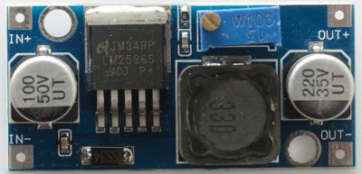
Additionally I added provisions to the board for a very common buck converter module. It contains all of the glue bits, and the LM2596 switching regulator. There is a really good write up on its output characteristics here.
Here it is pictured:
![]()
The ripple that is advertised on these modules is grossly underestimated, actual is closer to 200mVpp. Additionally the regulator does not hit unsafe heat levels at 1A, but would absolutely cook itself running at the advertised 3A! I recommend not running the regulator much past 1A but, if 2A is needed a heat sink and proper case ventilation are an absolute must. I installed the regulator on the breadboard build and found that the whole initial build on the breadboard never reaches anywhere near 1A. In fact actually only 225mA. This means technically it will run off of the 500mA supply provided by my USB to TTL converter, but as the final build has some expansion I felt the switching regulator was a must. As I am still waiting on PCB's I haven't done amp draw on everything as it would be including the interface card, I can only guess at 230mA is probably fairly close. When I did the layout I included a small prototyping space below the area where the module is mounted, allowing for air flow, as well as an option to build up a switching regulator or to use a compact regulator if that is the choice of the builder.
The layout:
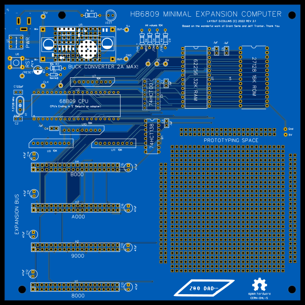
![]()
So this thing is truly a labor of love. I wanted to initially try to keep the build size on all of the cards to be sub 100 mm x 100 mm, however I couldn't make all of the slots fit in a usable configuration along with the CPU and ram so I ended up pushing the board size out to 160 mm x 160 mm (mini ITX). The bottom slot (H8000) Just fit in front of the 1 allowed expansion card space for that form factor. The remaining slots fall in line with the IO shield section of the board; and so would need to have their IO brought out to the shield if this were to be put into a case.
If there is interest, maybe I will make a mini-frame, with a CPU/ROM/RAM card to get the cost down further. The increased size means the board cost is around 15 dollars + shipping from china. I did not check the US based rapid turn prototype places, so that might be an option if somebody is interested.
I pulled all of the routed signals out on test points, or to pull up resistors for easy access if somebody needed to bodge in an extra route to one of the /INT* signals on the expansion slots. I added useful test points for the system clock, E, /RESET and all of the power rails. I was careful to allow for a rather large ZIF slot for the option ROM, so that swapping it out can be trivial if somebody would like to use one. Lastly I included a large prototyping space, more than large enough to build whatever expansion you have in mind; it's close to both the address decode logic and the slots so bringing over a select line is trivial. I built power rails on three sides of the area, and brought +5v and GND test points out near the prototyping area so these can be activated in any way you see fit.
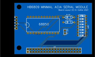
I also built a small ACIA card:
![]()
I put a set of DIP switches on there, to set the interrupt channel if desired, as well as the ability to route the interrupt line directly to the CPU.
Conclusion:
Hopefully, the PCB's will arrive soon and I can start building this thing up. Its safe to assume I am excited to get started! Inevitably its almost assured somebody will want to know the build cost. The PCB's were around 50 dollars shipped from china, this is likely the highest cost -- if you are building one of these up it would be in your interest to find a friend with a board or go together on shipping to keep the cost low. I did not check the US board makers, the costs are typically higher (with lower shipping cost). The passives including the crystal I had on hand but I estimate the cost for passives at less than 2 dollars if you pay for low cost shipping, or can bundle them with the rest of the chips. The logic chips were 2-3 dollars. The CPU and ACIA are around 5-9 dollars a piece, get them both from Jameco so that you are assured non-fake parts (usually). The RAM and ROM were 3-5 dollars each, the connectors are likely the largest parts cost; I have not priced them out yet but even using a standard 40 pin connector (that is on every raspberry pie ever made), I wouldn't be surprised if it wasn't 15 dollars for connectors and the regulator board. Given a lot of us seem to have some of this stuff kicking around already, it might be easy to get the build cost WAY under 100 dollars if you are careful how you go about it. Another thought, there is no reason you can't build this to use all CMOS parts using the 63c09, though you might need to change the firmware in order to get it into compatibility mode.
- I wanted it to be low cost ( not made of money, retro kits are expensive lets be real somebody has to pay for the time and energy that goes into making these things into kits, documenting them, distributing them etc.)
-
Here's the plan...
07/19/2022 at 05:33 • 3 commentsHere we go.....
![]()
So I needed a pallet cleanse of my CMOS CPU project that's kind of hit a snag. I bought this 6809 in a vintage electronics suppler that is about 40 minutes from my house called Chester electric. They are a small electronics suppler and they have everything! Seriously from HAM parts to boards you can buy to pull micro's off of; it is my happy place. I never manage to take pictures when I'm there but here is a video Rinoa's Auspicious Travels took of the inside of the place:
if you are ever in southeast Wisconsin its a very interesting place to visit, I highly recommend it!
The CPU:
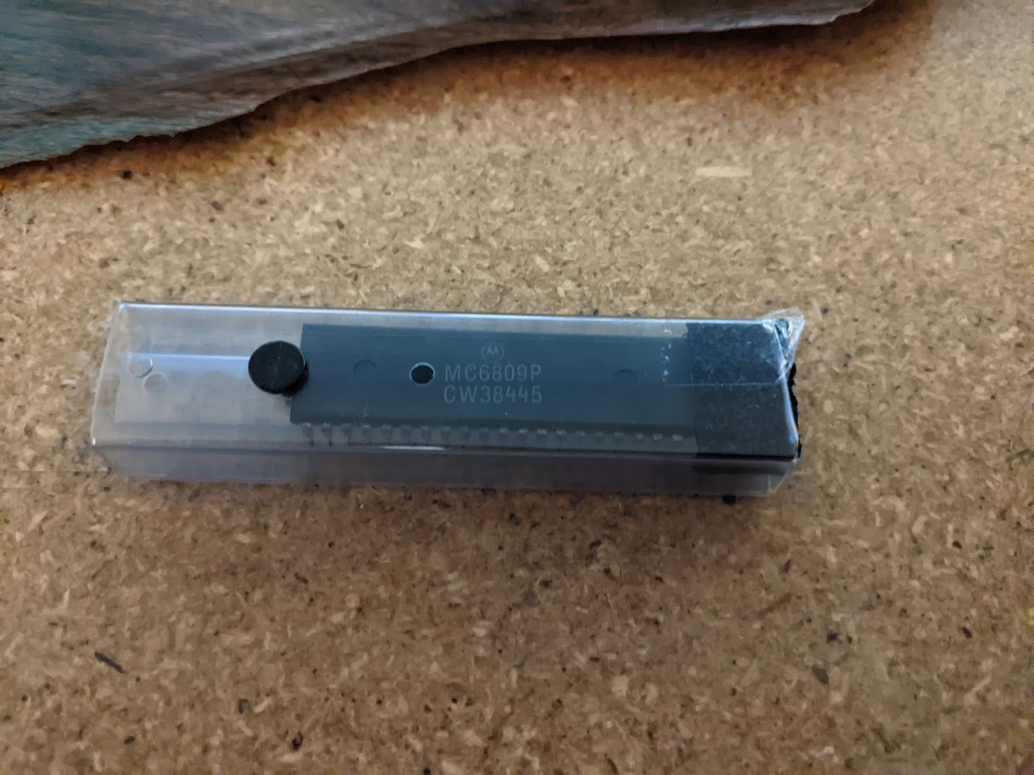
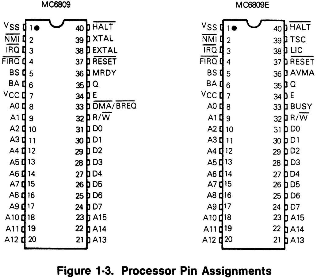
Its important to talk about the different types of 6809's. As far as I can tell there are 3 speed grades B, A and standard (68B09, 68A09, and 6809) these versions have a "On chip Clock Circuit". Additionally, there is a E variety that brings the divided clock outside of the chip. This computer uses the on chip clock variety. By way of comparison, the Tandy Color Computer (CoCo) uses the E variety All of these chips end with E[Package Type] and so they would be: 6809E, 68A09E, or 68B09E. The package type labeling varies but simply put P = plastic or C = Ceramic, and vice versa. Also, as a word of caution, it is easy to confuse the chips as they are all 40 pin packages but the pin outs are greatly different. There is an adapter available although I've not tried it and have no idea if it works well. Here's a cross reference of the CPU's I shamelessly ripped from google image search from this source:
![]()
The plan:I'd like to build a basic computer (at first, though I'm not limiting myself). I'll base the initial build off of Grant Searle's 6809 basic computer. If you've never been over to his website you really should its an invaluable resource. A while back i built a terrible first attempt PCB of his keyboard and TV interface.... i'll not link it here as it's not a very good example of the design but if you look hard enough I'm sure you can find it.
Grant has spent a lot of time and energy on his website, so if you want schematics for his original build, he's asked everybody to not re-post them so head on over there to take a look.
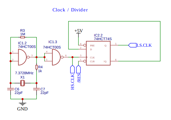
To start I would like to improve the clock circuit. Since the chip has an internal crystal oscillator amplifier pin (XTAL), grant simply used it with a crystal and two capacitors. This arrangement is actually specified in the datasheet, however, since there are 3 speed grades of the 6809 (non-E Version) it is nice to have a little divider circuit so that we can use the lowest and highest speed grade with a jumper and 1 crystal. Since were using an ACIA as a the initial display and user input interface, it is fortunate grant selected a 7.3728 Mhz crystal for his design. Simply, with that clock frequency we can get a baud rate of 115200 out of the AICA. However, by building a clock that can both supply a perfect clock for the serial interface and also optionally divide itself down to provide something closer to 4 Mhz ( ~3.68 Mhz), we can use the lower speed grade chip without harm. Additionally the CPU divides down the clock further, by a factor of 4. So in the end we get approximately 1.8 MHz. for a B speed grade chip and .9 Mhz for a standard 6809 (this sounds slow but compared to chips of the day it's actually right in there).
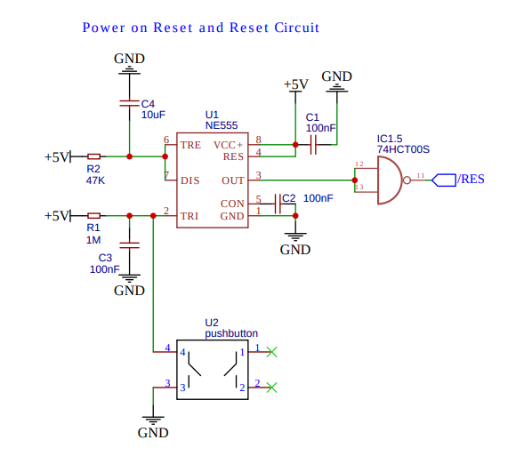
Since grants design, does not have (or really need for that matter) a power on reset, I had to add one for the clock divider in my clock. And so I went with the standard, substandard, C64 Reset Circuit:
![]()
For the simple reason I've used it before, and it works. I may experiment with one of those reset chips, that provides watchdog / brownout protection, but for now this is a very common known design. Since I had to put in the inverter chip any way (actually its a NAND), I used two more gates to build a more standard clock Circuit:
![]()
This gives me 2 clock Signals I can select for the main system clock, and a High speed (full speed) clock for the AICA (or really other peripherals that might need it.) I added a jumper block to the schematic with a PCB footprint so I can pick between the two for the main system clock if I decide to have PCB's made, at this point were just building on a bread board. Using this single pin configuration, the data sheet specifies we can ground the XTAL pin and connect a TTL compliant clock source to the EXTAL pin, so when I do the CPU module I will need to take this into consideration. The biggest concern is keeping the clock lines VERY short to prevent ringing; I may need to attenuate them if this becomes a problem.
 Dave Collins