 Jesse Farrell
I recently saved a faulty PSU from the landfill, but I inherited a new project as a result. The device is a “Topward Electric Instruments Co., LTD / Model TPS-4000 / Dual-Tracking DC Power Supply”. This is an old and sturdy power supply with a surprising amount of weight behind it (or perhaps not surprising given its vintage).
Note – I’ve organized this post somewhat backwards: the key fault/solutions are shared first followed by the troubleshooting steps that led me to these findings.
Solution
- Burnt Parts – Generally need to be replaced but not necessarily “the” issue
C10 – 0.22 µF 250 V Mylar Capacitor, that connects master negative to chassis GND. C23 – 0.47 µF 250 V Mylar Capacitor, which might be playing a dual role to suppress transients seen by U03 while simultaneously slowing the response of the tracking mode configuration. R40 ×2 – 10 kΩ Metal Film 0.25 %, used as a resistor divider for U03 when in tracking mode.
- Scratchy Potentiometers – Replace R08 & R12
Both CC/CV potentiometers are in varying states of decay causing sporadic changes in their resistance. I had some success cleaning with isopropyl alcohol, but decided to swap them out entirely in the end. I grabbed some footage of the “scratchiness” – take a look below.
- Faulty U02, 741 Op-amp – Replace Faulty Component
This still has to be tested/validated. The inverting input seems to be drawing ~3× more current than its rated maximum input bias current. As a result it’s dragging the voltage at the input low with respect to the non-inverting input.
Pending Work
- Test U02 fault op-amp theory - DONE
- Replace C10/C23/R40/R08/R12 - DONE
- Calibrate PSU - DONE
Troubleshooting
The TPS-4000 “Slave” channel is faulty. The symptoms of this fault are as follows:
- Sporadic voltage jumps, typically while adjusting CV / CC.
- Fast relay clicking typically during adjustments (changing voltage ranges).
- CC mode engaging intermittently (sometimes getting stuck – I didn’t actually notice this until later).
- Oddly, most of these issues disappeared in tracking mode.
Faulty PSU Before Repair – https://www.youtube.com/watch?v=vE3p9F3KMP0
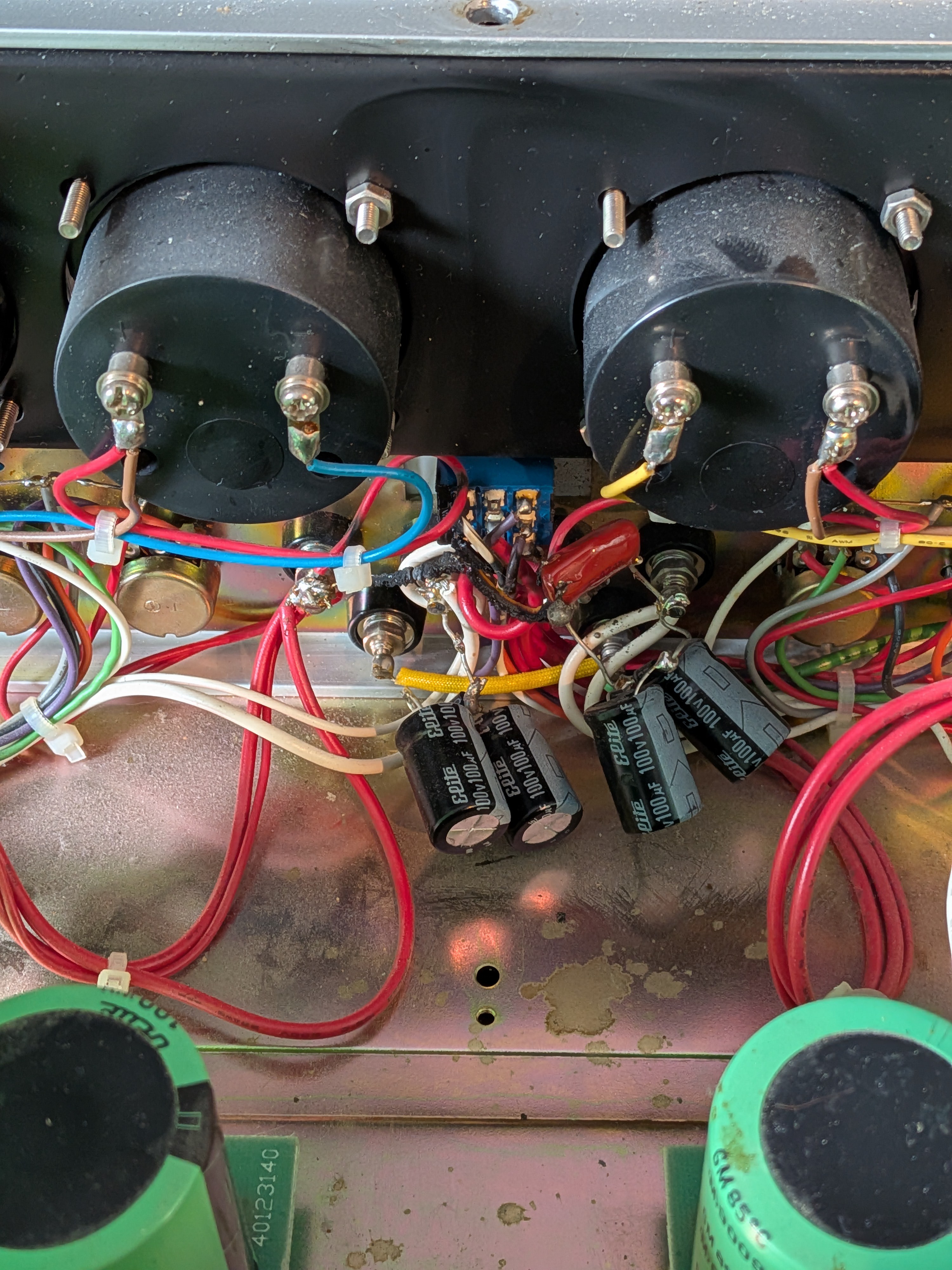
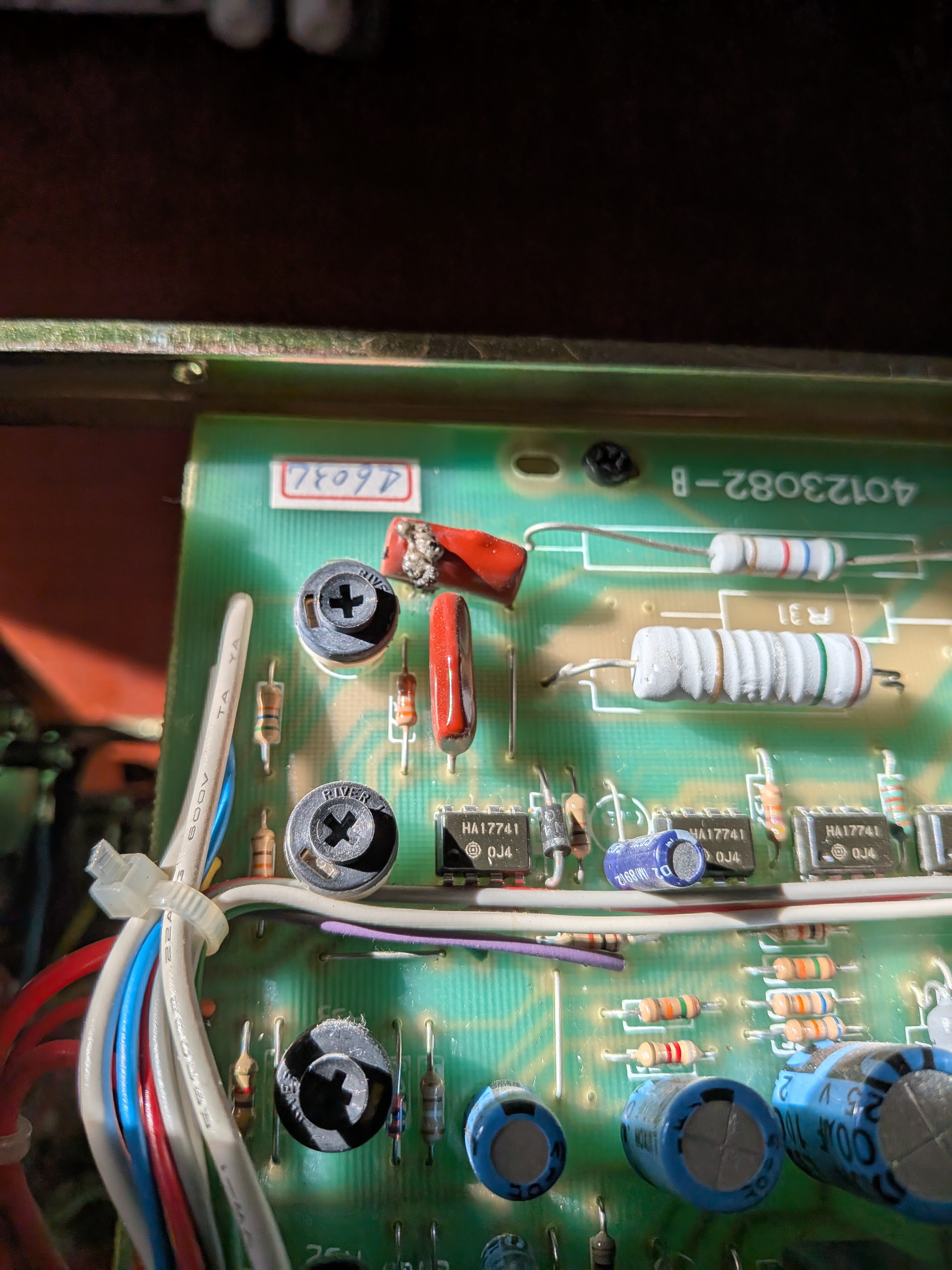
The first and most obvious fault was a blown film capacitor and some burnt wire on the back of the front panel. I later found one more bad film cap on the “Master” channel, this time mounted to the PCB. After going through a visual inspection I checked that both channels of the PSU had all their rails present. I also verified some key transistors and diodes weren’t blown.
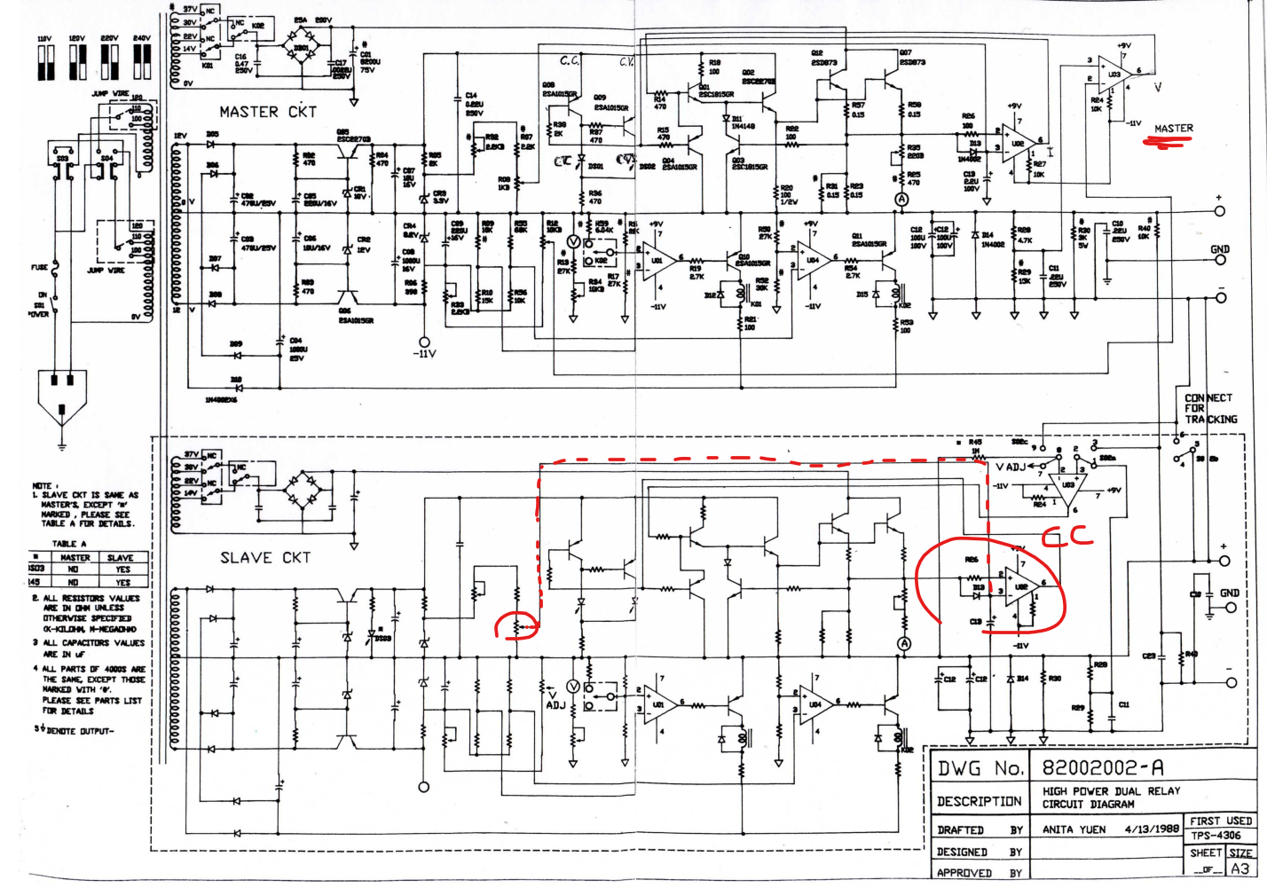
I started to go down a few rabbit holes to understand where each terminal of the rocker switch (which seemed to be the epicenter of the burn) connected to. Luckily, I managed to find some schematics online, saving myself having to reverse-engineer the circuit (maybe next time…). The schematics aren’t for my exact model but it seems close enough.
I’ve heard of scratchy potentiometers but I’ve never actually seen one during my repairs. I opened up the pot casing and cleaned it with isopropyl alcohol. The results speak for themselves.
Video before cleaning
Video after cleaning
Having repaired the scratchy potentiometer, the output was now MUCH more stable. Now the unit remained locked in current limiting mode, despite the lack of loading on the output.
For a while I was convinced that U02 was COMPLETELY HOSED… But later found I was being misled by the schematic. All op-amps here are exactly the same 741-op-amp, but the schematic labels U03 differently from U01/U02/U04. The correct labeling has the inverting input as pin 2 followed by the non-inverting input on pin 3. This means all U01/U02/U04 are mislabeled. Knowing that I was probing the incorrect node subdued my U02 suspicion, but not for long…
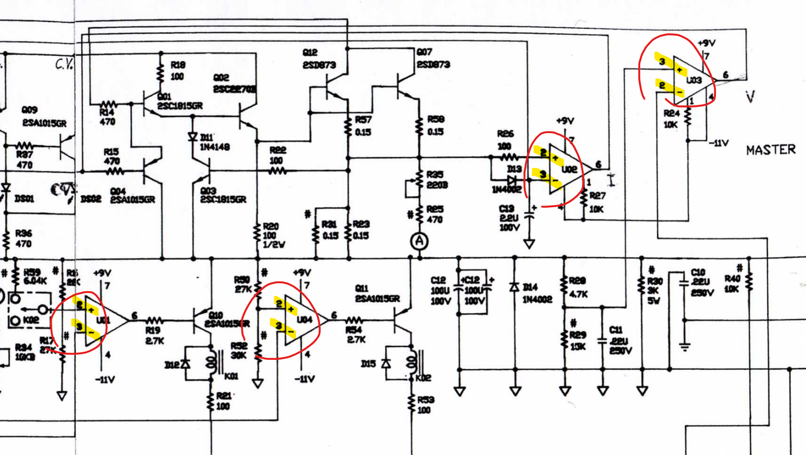
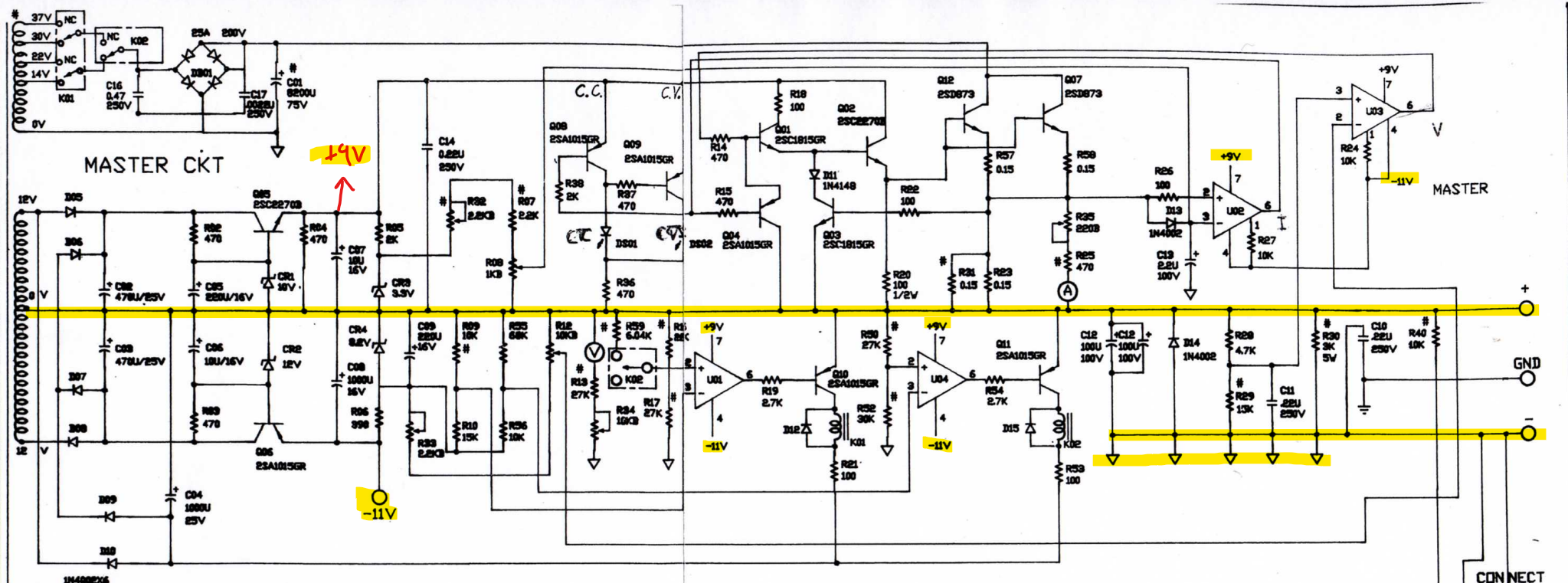
Before I get to the new issues with U02, I’d like to take a short tangent to talk about the signal GND and referencing on this schematic. On the left side of the schematic a +9 V and -11 V rail are generated from a ±12 V center-tapped transformer. This center tap is connected to the positive output of the channel. This means all of our op-amp voltages (and other components for that matter) should be measured with respect to the positive channel output. This is somewhat confusing since the negative output was given the signal GND symbol. I don’t think this is particularly wrong, but it definitely caused some confusion. Just looking at the screenshot below, you’d be forgiven to think you would measure +9 V on U02 pin 7 w.r.t the negative output of the PSU (but you would actually see Vo +9 V).
Back to the issue at hand: U02’s inverting input. The node was being held below “GND”. Since no current is flowing the non-inverting input sees “GND”. Since the inverting input is below the non-inverting we expect the output to be driven high, putting the PSU into current-limiting mode.
All of this is expected. So why then is the inverting input causing this behaviour?
Comparing to the good Master channel, its inverting input sits closer to 0.5 V. Calculating the current going into the op-amp showed a consistent ~1.8 mA. Oddly, maybe even suspiciously, high for an op-amp. This flavour of 741 has a maximum input bias current of 500 nA (oh boy).
An interesting find was that R07 is larger than it should be. The schematic, and the Master channel, use 2.2 kΩ; however the slave uses 3.6 kΩ.
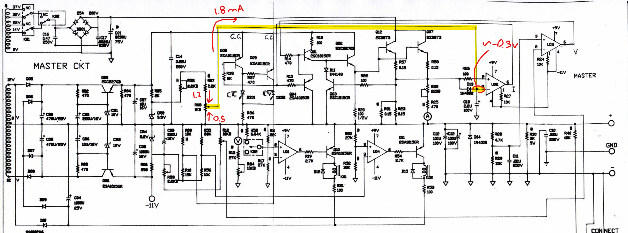
I tried to compensate for the increased bias current of U02 by tweaking the value of R07 and R32. Sadly the resulting compensation loaded CR3 too much. Furthermore I’m suspicious the bias current is somewhat unstable, since I can see CC mode being asserted briefly while operating.
Next steps…
- Test U02 fault op-amp theory.
- Replace C10/C23/R40/R08/R12 – Parts arriving soon.
Update - Nov.2.2025
The PSU is now fully repaired and calibrated. The final issues / fixes are listed below.
| Fault | Comment |
| U02 Faulty - Increased Leakage Current | Increased input bias current was pulling one of the inputs below GND. Causing the slave output to constantly assert current limiting. Swapping for a new 741 resolved this issue. |
| Scratchy Potentiometers - R08/R12 | Several pots were horribly scratchy. These scratchy potentiometers directly fed opamp inputs leading to sudden unpredictable changes to the current and voltage set-points. I ended up swapping all 4 pots, though cleaning them would have also worked. |
| Burnt Components - 2xR40/C10 | 3 components were badly burnt along with their wires. These formed the tracking mode divider. I replaced both R40's with a 47k instead of a 10k.... since 65V^2/10k = 0.42W is a bit too much power for these cheap resistors. In contrast 47k will only dissipate ~0.1W max. |
Discussions
Become a Hackaday.io Member
Create an account to leave a comment. Already have an account? Log In.