 Dave Collins
What’s next?
We’re still chugging along on the VZ200 clone, building it out as a set of RC39‑style modules on a back plane, all as part of our open‑hardware project with PCBWay. A bunch of the boards are already up and running, and the machine now boots into a serial ROM monitor where I can poke at RAM and ROM, its early days however things are progressing nicely!

But
then I hit a snag with the display memory circuit.
So
this is the story of what happens when you take a simplified 1980s
chip set and try to squeeze it into a GAL to save board space and a
bit of cash. Let’s walk through what it actually takes to get this
tiny display module to read and write its RAM chip the way it’s
supposed to.
The
VDG problem:
Last
time we talked about how the 6847 expects bus arbitration pulses to
clear its address strobes off the bus so the CPU can write to memory. We went over how this creates snow artifacts as the 6847 tri-states
the address bus outputs. We also went over how the timing of the
specific logic inside the circuit is paramount to making sure the
6847 is off the bus so that the CPU can make an uncontested write
operation.
The
Schematic:
But what if we don’t want to use LS logic from the 1970s to accomplish our video module? Let’s go over the video circuit in detail by looking at the schematic.
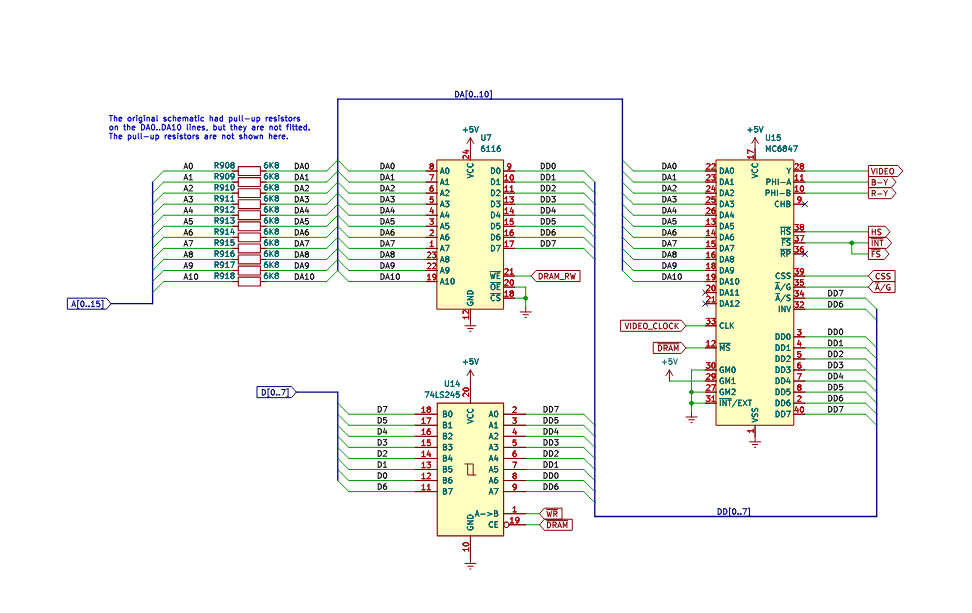
We
see that the data bus is separated by a bus transceiver, from the
6847 (VDG – Video Display Generator) and RAM chip data pins. Going
over what we know about the VDG from the last time, it has to strobe
through all of the addresses on the RAM chip and build a raster 60
times a second no matter what. That's because the 6847 isn’t
really a video display processor, it’s a finite state machine (FSM)
with selectable states. Some of these states are selected by data
pins, and some are selected by separate control signals from an
external register typically (in our design they are). The VDG really
only knows how to run a few tight loops: scan the RAM and display in
text mode, scan the RAM and display in graphics mode and so forth. These “states” in a fixed path tight loop are what makes the VDG
a state machine and not truly a dedicated video co-processor. Essentially, it scans the RAM really fast and pushes out a bit
stream, as well as create all of the relevant sync and color
information pulses over and over; forever, unless you change the
state or interrupt them. Think of it as an elevated version of the
“TV Typewriter” but with much of that circuit already built into
the box, including the character ROM!
The
Crux of the Problem:
So we have established, essentially, the circuit has to keep the data bus and the address bus clear of contention whenever the 6847 needs to push out a frame to the display. The circuit does this by separating the address bus with a bank of resistors, and the data bus with a bus transceiver. When the /DRAM signal is generated in the chip set the address bus on the VDG cuts out, the data bus aligns with correct directionality, and the RAM chip is selected. Ultimately this creates snow because the CPU does not know when the VDG is on the RAM it only knows it can knock the VDG off the RAM by writing to or reading from it. This works well, it’s simple and cheap but obviously the issues are:
- Timing is tied to the logic family, and the specific construction requiring multiple chips
- Even though the CPU and the VDG are clocked by the same clock, they are not synchronous. The Address decode, write and read cycles of the Z80 prevent the two devices from truly being able to avoid contending with one-another.
- The VDG is knocked off the bus on every single write and read to the display memory, this “second fiddle” bus positioning means lots of artifacts.
- Artifacts are annoying and they can ruin user experience.
- The decode circuits cascade decoder chips, which leads to large propagation delays that are hard to replicate, and sometimes required to make the circuit work.
- Even though it’s minimal, it’s three separate chips and supporting chips for bus arbitration as well as latching data. This takes up a lot of space on a module, and we have to replicate that design multiple times, or use the USR lanes to move signals around the back plane.
To sort all of this out, we’re going to re‑design the circuit so we can get rid of most of the headaches by using a GAL and some dual‑ported RAM. It sounds a little intimidating at first, but as you’ll see, it’s really not that bad. And the nice part is that by mixing these two bits of tech, we can simplify the whole design and even make it a little smarter without changing how the computer actually works.
The issue with GAL:
GAL devices (Generic Array Logic) are PLD’s (Programmable Logic Devices) with a smaller number of units typically used to integrate (or reduce) discrete logic chips in designs. One of the core issues with replacing a bunch of logic IC’s with GAL is that the propagation delay is reduced.
That's right, I will say it again because I think it’s important. When you replace logic IC’s in a design with a logic array, the propagation delay is reduced.
This
seems on the surface a good thing right? But lets break this down. In part one we discussed how the timing delay generated by the final
OR gate is used to create a 22 ns delay between when the address bus
goes to tri-state on the VDG, and when the RAM IC is selected to
store the value from the CPU. The fact of the matter is; simply
put if you just replicate the circuit inside a GAL, the two select
signals can become so close that you could very easily have data bus
corruption. So what do we do?
GAL
Based Graphics Address Decode and Registers:

Well we start by breaking down the decode circuit to simply just the logic we need. For simplicity’s sake we build it again in H. Neemans Digital. Since “Digital” will simplify the logic to just the logic we need we don’t have to pay too close attention to the specific make up of the logic devices we are using as it will break it down into the simplest equation automatically, more on this later. We can go into the properties of each input and output and assign a pin to each, our device is a standard GAL part known as a 22v10. Its capabilities are specified in the data sheet but for simplicity sake we will say this device has enough logic units, and we’ve picked pins that will be compatible with the device.
We next build a register, for the two control lines we care about on just the graphics module. A register lets us clock the internal latch on every clock pulse, in our case we will clock it on the falling edge of the /WR line during any memory access cycle (pin 23 loops back into pin 1, the chip's Q input). Clocking the register every memory write cycle seems less than ideal, won’t we end up with a bunch of data we don’t need?
When
I started with electronics the difference between a latch and a
register kind of went over my head a bit. It took a while to see the
difference. With a register we combine a multiplexer with a latch so
that it can latch two things, the register’s own value, or a value
we want. The multiplexer lets us decide when to latch the data we
want. With a standard latch, we only latch what is on the data pin,
and in effect only one part of a fully functioning register. For
just the two bits inside the IC it takes up a lot of combinatorial
logic. Nearly the maximum for each logic cell that we use for these
two registers; but we need this functionality to pull off some really
cool linear processes. The end result is that the register will latch
its own value on nearly every write operation (and therefor hold it)
until we tell it with the decode logic to latch from the bus. But
the reason we need a fully fledged register is we also need a third
latch that catches something called /WAIT at the falling edge of
every cycle. But before we discuss /WAIT lets talk a little about
dual port RAM, and why we are going to use it here.
The solution, dual port RAM:
Dual-ported SRAM is basically traditional SRAM with one big twist: it has two independent ports and built-in collision detection. Collision detection allows the chip to generate a /WAIT signal on each port when a read or write operation starts on the other port, accessing the same memory cell (address) that the other port is accessing. When this occurs we get a /wait signal for the port that is late to the party. Each port has a wait signal and so we call them /WAIT-L and /WAIT-R. Consequently the data ports are also labeled left and right, but they are located in whatever orientation the designer desires when the board layout is done. This logic detection behavior is also first come first serve, so whichever port starts its read or write operation first wins access to the cell.
When two devices read from the same memory cell, there is no contention it simply splits the data path and shows that data on the bus on both sides of the chip. The device still generates a wait signal but it can be ignored if both ports are being read from. However, if you try to write on one side after you have already tried to read from a cell on the other side of the chip or vice versa you can get into a mess. In practice it is safer than our single port design. Truly if you try to write to an active data cell with the part we are using there is no contention, although the data is dropped and not latched, leaving whatever value was last stored there instead. This behavior is actually worse than the snow on the previous design, because the written data is lost in that case, and the display file can get corrupted resulting parts of the screen not updating correctly.
The solution is we need to check before a memory latch, if there is going to be contention from the VDG’s reads when the CPU needs to write. Furthermore, we need to shut down the chip select on the VDG side of the display memory, but only if there is read contention from the VDG. Lastly we need to hold it that way until the read operation is over. We don’t have to worry about reads because the VDG’s data port is wired in such a way it only reads from the display memory, and as previously discussed we don’t actually have to worry about situations where both devices read the same cell.
So then, what we need to do, is create a circuit that on every memory write, it captures the status of /WAIT (which we get by doing a logical AND operation on /WAIT-L and /WAIT-R). Furthermore, this must happen before we latch the data inside the memory. Also we have to only really do this when it makes sense, within a video memory write.
On
the surface that seems like a very tall order. We have to have a
circuit smart enough to make a decision on every write operation, we
have to have a way to detect the address being accessed to see if it
matters, lastly we have to know if it is a write cycle so that we
only clear the contention when we need to, because as we have seen
doing so on every write, will cause snow. At first cuff, this looks
like a task for a CPU, or even a very fast micro-controller. That's
a lot of decisions to make, but you’d also be hard pressed to do so
on even a fast micro-controller in the context of a memory write, on
every single write. But fortunately we have a GAL with some free
cells sitting on our design, logic units are fast and we can take
advantage of that by building a small state machine that can handle
the tight loop of checking without even breaking a sweat. But first
we should talk about the Z80 write cycle.
Z80’s
Write Cycle oversimplified:
Alright, let’s talk about the Z80 write cycle, because the timing here really matters. The write cycle starts in T1, and by the end of T1 the address bus is already valid. That’s the moment the rest of the system can trust the address lines and start reacting.

Then we roll into T2, and this is where /WR drops. That falling edge is the CPU’s way of saying ‘okay, this is officially a write now.’ From that point on, the data bus is settling into its final value, and the memory is getting ready to latch it.
The important part is the window between /WR going low in T2 and the actual data‑latch moment in T3. This is a small window where we can insert just enough logic to shut down a memory read on the VDG side, so that when the rising edge of /WR happens in T3 everything is good.
That’s the whole reason we care about the exact T‑state boundaries. The Z80 gives us a predictable sequence, but the hardware around it has to behave inside that little T2‑to‑T3 window if we want reliable writes.
This small window between when /WR goes low and /WR goes high, just so happens to be the perfect amount of time for our little state machine.
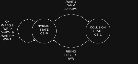
By grabbing the AND result of both wait signals on the falling edge of /WR and /MREQ, we can tell whether there’s a collision before the rising edge when the data actually gets latched; from there, the GAL can drive a pin that disables the VDG’s data port on the dual‑port RAM. In other words, we end up with a tiny state machine that watches each write, checks for contention, and, if there is any, temporarily takes the VDG off the bus so the write can complete cleanly. We basically add another state to the VDG that only kicks it off the bus in the event there is actually going to be a collision. The result is very tiny, basically imperceptible artifacts, that are constrained to a single frame. We don’t eliminate the artifacts, we just prevent them from being viewed by the user, as they can only last for three T states maximum.
It’s also important to understand that the latched /WAIT bit in the GAL does not directly store the /CS value; it stores the collision status (/WAIT) for the current write cycle. /CS for the VDG port is derived from that state, and it is cleared on the rising edge of /WR. In other words, as soon as /WR rises, /CS drops again, regardless of what the latched /WAIT value was. The collision state only ever lasts for a single write cycle.
Additionally,
because all of the behavior is edge clocked, there is no need to be
concerned with the specific timing of each part of the circuit; we
fixed our GAL timing problem, reduced footprint size and improved
memory contention artifacts so they aren’t visible to the user (yay us!)
Getting H. Neeman’s Digital to do the Hard Work:
Digital can do some fairly amazing things, but one of the coolest things is the circuit analyzer. It will break down a combinatorial and sequential logic systems into both boolean algebra, and a truth table. But it also can then take those two things, and through its synthesis menu you can have it build both the CUPL file and the JEDEC files for GAL production. In other words, you don’t have to bust out WinCUPL and actually write your .CPL file, digital simply does this for you.
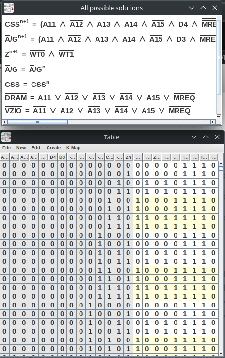
There
are some limitations, for instance it won’t let you use a IO pin as
anything other than an input, and the stock version of the program
only lets you use the Q pin as a clock input (though I patched that
for my project). For our purposes this is perfect. We don’t need
so many outputs by modularizing the design, we can get around the Q
limit by simply patching the open source program so it works for us. You do have to understand the pin limits on your specific part and
tell Digital which inputs and outputs belong to what pin, but
it’s just a context menu operation.
For visual people like me this is a godsend.
Whats next?
Up next is a deep dive into the banked ROM/RAM card, and specifically how you lay out a 128K RAM chip in a computer that is meant to have only 6K of RAM. Again, I am doing this work in my spare time so it may take a bit for the updates.
Again I would like to thank PCBWay for helping us with the prototypes for this project. I have worked with them for years, and I would love it if you would check out the services they have on offer. I recently shipped a bunch of boards in from China, and despite the shipping situation in North America right now, the pricing was completely transparent, and in the end there were no nasty surprises. The shipping options were clear and concise and you can easily tell which shipping options include duties and fees, and which ones might still hit you with extra charges. This really took a load off of my worries about all of the work and cost going to waste because of some technicality, this simply wasn’t the case.
I want to thank you for coming along this far, and I hope you do check back for more updates as we progress. Please don’t hesitate to drop me a line if something piques your interest in this design. We are coming around the bend on this one and hopefully soon I will have a working computer.
Discussions
Become a Hackaday.io Member
Create an account to leave a comment. Already have an account? Log In.