 Samuel A. Falvo II
I'm happy to report that, inside of a Verilog simulation, the KCP53000 has run its very first program. Kind of.
I'm being somewhat unfair though; see, the circuit consists of the CPU coupled to a simple ROM which is direct-wired onto the I-port of the processor, while the D-port is hard-wired to the value $41. So, when this program attempts to print its "Hello world" message, all it prints out is a bunch of "A"s. So, in that respect, the processor is doing exactly what it should be doing.
What's missing is a Wishbone bus bridge which I can use to couple the D-port to the same ROM image. Additionally, I'll be needing a Furcula bus arbiter to funnel both I- and D-ports into the same Wishbone interconnect. Once I have that, I can then perform address decode and mapping of ROM and RAM, and both should be equally accessible for instruction or data access.
I've worked up a conceptual model of the Wishbone bus bridge.
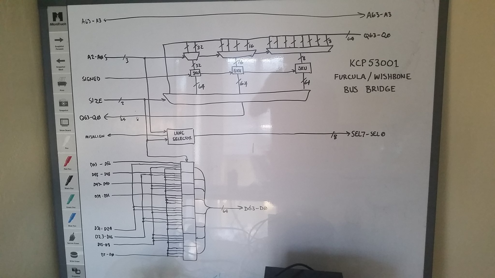 As you can see, it is largely an arrangement of multiplexors and zero/sign-extension units. The most complex part of the unit is going to be the byte lane generator, which is really a 32-minterm piece of logic that generates Wishbone's SEL_O signals as well as an error indicator back to the CPU, MISALIGNED (which I'll ignore for now, since CPU doesn't yet have such an input).
I haven't quite figured out how to implement the bus arbiter just yet. Since I know that the KCP53000 cannot yet overlap its bus cycles, I might just logically-OR all the buses together and go with that for now. However, when I implement fetch/execute pipelining later on, that approach will fail spectacularly. However, with the SVFIG Forth Day and 5th RISC-V Workshop just around the corner, this stop-gap just might be worth the do-over later on.
Discussions
Become a Hackaday.io Member
Create an account to leave a comment. Already have an account? Log In.