 Eric Hertz
Oh man... I looked and looked, and the best I could find was the ol' 8255 (GPIO/Bus expander for x86's)... which woulda been great, but even the updated versions are quite slow...
And then... months and months later, I don't think I was even looking for it, just stumbled across it somehow... The 74x[16]543 came to my attention.
I knew there had to be *something* like this, I just couldn't seem to find it, before.
My original plan for a "professional" design was basically a D-latch (the all too common '374 or the much nicer-pinouted '574) to write data/commands and a Buffer with output-enables (equally-common '244) for read-back. In the case of the bidirectional '543, an additional latch wouldn't hurt (in the read-back portion)...
But, dang, I'd already put a LOT of thought into how to make use of the SDRAM's inherent technologies, e.g. DQM is *kinda* like Output-Enable... And now with CKE it's possible to "latch" the outputs for as long as I want. I really only need a D-Latch bypassed with a resistor for each bit, even combining all that onto an 8-bit bus.
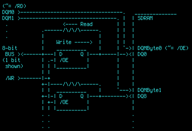
The other benefit is fewer control-signals... With a bidirectional D-latch (or even D-one-way + Buffer-the-other) we need, at the very least, an additional /RD = /OE signal for each byte.
(Unfortunately, in this case, DQM is used for both-directions so can't be tied *directly* to the read-back buffer/latch's /OE. And, DQM is necessary for other purposes as well.)
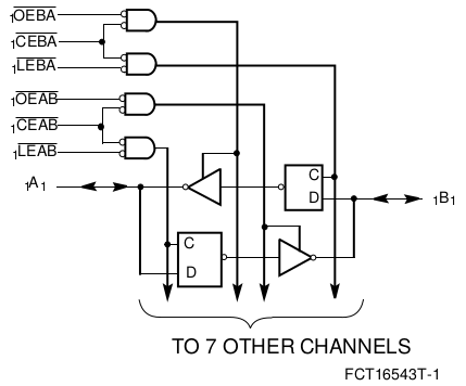
Look at all those control-signals! Whew! But, some of them can probably be tied low... Others may be tied-together via inverter.
So, it's a debate... Roughly: each byte would require:
D-Latch + Resistor:
- 74x574 (plausibly 573?)
- 8-gang network-resistor
- DQM signal
- /WR signal
Bidirectional-D-Latch:
- 74x543
- 1-gang inverter
- DQM signal
- /WR signal
- /RD signal
Resistor-bypassing might be a bit slower
- takes some time to overcome pin-capacitances
- the 8bit bus is generally going to be slower than the SDRAM, but needn't be *artificially* slowed
Bidirectional D-Latch comes in speeds of 7ns or less, (144MHz!)
Also is a bit more "professional" (aka "Not A Hack").
Cost-wise, probably not a whole lot different either way, but the bidir-D method is plausibly slightly cheaper, not needing network-resistors.
Resistor-bypassing uses extremely common chips available in my collection and probably many others' (or could be stripped from old ISA/PCI cards, motherboards, and elsewhere).
If I'mma buy chips, the Bidir-Ds make a lot of sense, especially the 16bitters... And... most of those chips in my collection are not nearly as fast as those available nowadays (same pinout, likely smaller packages).
At what point does a CPLD make more sense...? A few more pennies for an FPGA and Free-Running is no longer necessary... Wee!
The "Shit You Have At-Hand" factor is calling to me at the moment, anyhow. Nevermind breadboardability.
Discussions
Become a Hackaday.io Member
Create an account to leave a comment. Already have an account? Log In.
Confused? You won't be after tomorrows episode: "Eric makes a decision!"
Are you sure? yes | no
And here are the reasons why you should NOT go with FPGA and instead stay with basic logic:
1. While FPGA's are commonly available, they pretty much all require SMT soldering so users who can't do that would need to purchase a breakout...
http://store.gadgetfactory.net/papilio-one-250k-low-cost-xilinx-fpga-dev-board/
http://numato.com/mimas-spartan-6-fpga-development-board/
2. You getting bogged down in learning VHDL or whatever could actually slow down the development of this project, and lead you off down many other (abet interesting) paths. In fact, you are probably going to get bogged down making a better freaking break out board since nothing good seems to be available...
3. It may not be so easy to program an FPGA from the uC... Note the comments on this post:
http://dangerousprototypes.com/blog/2012/02/01/jtagwhisperer-an-arduino-jtag-programing-library/
Although a quick search of github finds some interesting and hopeful looking code:
https://github.com/mrjimenez/JTAG
https://hsbp.org/fuji
4. sdramThing should be about the sdram...
Are you sure? yes | no
Hah, looking at those first two links... guess I hadn't really considered the I/O counts! E.G. SDRAM DIMMs are 64-bits wide... the address-bus is 16bits, we've already exceeded the number of IOs on those FPGAs. Hmmm... So, then, in order to get rid of the necessity for "free-running" and directly-fed-back wiring, we'd need a whole FPGA (of these sorts) just for that. Then, talking about complex-triggering, that'd require another whole FPGA... The two combined would probably accommodate whatever "bus" topology, routing data to the host for read/write... Or scale back a bit and still use 74xxx registers, etc. for routing data... and plausibly limiting complex-triggering to only a select few bits (maybe 8 or 16). Otherwise, to handle the entire system, we might be talking BGA and hundreds of pins... and who knows what cost. Hadn't considered this, things to ponder. (Also hadn't considered the *speed* of these things... one of those has a 100MHz clock... I guess my (very limited) FPGA-experience way-back-when was with a pretty high-end FPGA, as it had LVDS, DDR, and various other I/Os.)
"Bogged down" is definitely in the cards with new endeavors like these!
Now that I think about it, programming the FPGA from a uC, as you mentioned before, e.g. to change the complex-triggering, if I understand correctly, probably isn't quite the way to go... the uC would have to *compile* the code, etc. Instead, probably, have preprogrammed trigger detection schemes and select/configure one (via i2c or something)...
There's some great links in there, thanks... Already learned a lot just browsing 'em.
#4: Right! :)
Are you sure? yes | no
Really interesting... I'm going to say that it's worth going to the FPGA... Here is my thinking:
1. They are commonly available these days, cheap, and getting easier to program
2. Having that resource at your side will make the rest of the development of this project go by so much faster. It's all (sort of) software at that point.
3. A FPGA on the final product will make it possible to do things like complex logic triggers for the analyser. E.g. "start sampling when A OR C AND NOT D OR C"... This assumes the uC could pass new programming onto the FPGA... and that should be no problem right?
4. YOU having access and familiarity with an FPGA is like putting a supercomputer in the hands of a physicist... you don't know what will happen, but you really want to see what they might come up with.
Are you sure? yes | no
Good calls... the complex-triggering thing has been a bit elusive... an FPGA would make that quite simple, and the complexity of the trigger could be quite astounding.
Haha, Thanks for #4, but I dunno if I'd go that far. I think for me it'd be kinda like having a supercomputer, except not having any ideas for programs that require anything more than a microcontroller ;)
Though, one thing that a suitable FPGA would enable is DDR++ (and maybe even USB2.0?)
Are you sure? yes | no