 Eric Hertz
So, check this out... In a (long-) previous log, I had the idea of making use of the SDRAM's DQM inputs to make it possible to connect all 32 bits (four bytes) of the sampled-data to a single byte-wide bus using nothing more than resistors (and, for when the logic-being-analyzed isn't capable of driving the load, 4 74x244's, or similar)...
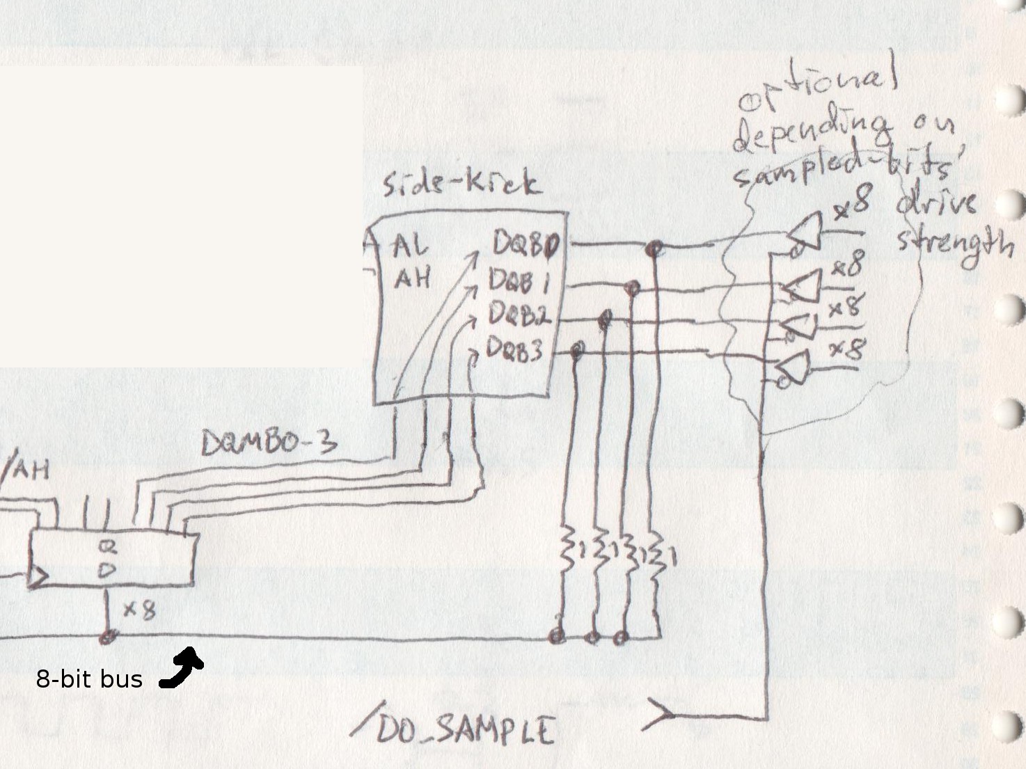
So, when the sampling occurs, the buffers drive the DQs... The outputs of the buffers are strong-enough to basically treat the resistors as open-circuits... (or, frankly, if the logic-being-analyzed is strong-enough, the buffers are unnecessary... but during sampled-data-read-back it's necessary to remove that logic-being-analyzed from the circuit... so the buffers' output-enables are handy. Nevermind, adding those buffers allows for e.g. making the "logic-analyzer" capable of various different logic-levels... 74AHC's or similar would allow for 5VTTL as well as 3.3VTTL... Others, plausibly in series, could make for 1.8V logic-analysis, etc. And, e.g. it'd be plausible to use 1.8V logic on 16 bits, tied to 3.3V logic on the other 16 bits and determine some intermediate-values for the same measured-signals.).
Now, per a recent log, I think it's possible to handle *more* I/O in a similar manner... Specifically: The Address-lines, which are *directly* fed-back to Data I/O's...
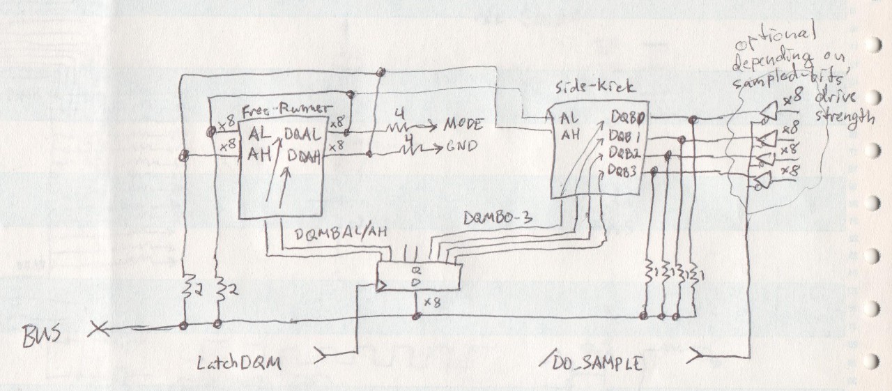
The address lines need a "default" value, as pulled-up/down by resistors, to make this possible.
The *only* "default" value they *need* is that used by the Load-Mode-Register command, so we set those bits accordingly, via pull-up/down resistors, and go on our way. (be sure to check that previous log-entry).
So, note... These resistor (networks) could be replaced with buffers... That'd be the logical way to go about it. But, doing-so, again, results in the necessity for Output-Enable pins for *each* byte. By using resistors we can take advantage of the inherent "output-enable"-nature of the DQM-inputs on the SDRAM.
("Hey! Why not tie the DQM signals *to* output-enable inputs *on* buffers such as the '244? Because DQM is used for BOTH Read AND Write commands... So, we'd *really* need another D-Q latch for *each* of those buffers' output-enable signals. AND FURTHER, using resistors allows for reading AND writing the DQ's (writing being a bit less-necessary in a logic-analyzer sense). )
The use of resistors, instead of logic, basically make for *bidirectional* communication, which would be a bit more difficult with glue-logic.
So... Where we at...?
I have yet to analyze *every single* case... but, having a vague idea of which cases we'll be making use of... I think this should work. Resistors marked "1" are, e.g. 1Kohm... Resistors marked "2" 2Kohm, etc. These aren't *values,* they're *multipliers*... So, maybe, I use 390ohms for the resistors marked "1" and 390*2=780ohms for those marked "2"... you get the idea.
(As the resistance increases, so does the delay in overriding input-capacitances, etc... is that a problem...?)
Anyways, the key, here, is that different *modes* treat these resistor(networks) differently... And, so far, it seems that *each* mode can work with this system.
- Free-Running...
- This is the mode where DQAH/DQAL -> AH/AL. This is *also* the mode when sampling of the logic-analyzer bits will occur (written into the side-kick, plausibly through the buffers enabled by the /DO_SAMPLE input).
- In this case, the "bus" value is of little importance (and should probably be Hi-Z by the "host")
- None of the *connected-through-resistors* bits interfere with each other (right?)
- DQ_AL -> AL
- DQ_AH -> AH
- Input-buffers on Bytes 0-3 go to DQB0-3
- Write to AddrH/AddrL
- DQB0-3 are High-Z (Via DQMB0-3)
- DQMAL/AH (opposite that being written) is active, allowing write to *only* the selected AddressDQ's
- A resistor of value "2" overrides that of value "4"...
- Read from AddrH/AddrL
- DQB0-3 are High-Z
- DQMAL/AH allow read from *only* the selected AddressDQ's
- DQ-values are written to the "bus" via a resistor of value "2", overriding the "default" resistors' of value "4"
- Read from "Side-Kick" DQ's (reading back sampled data)
- DQMB0-3 are set, except for the *selected* byte, so only the *selected* byte outputs
- DQMBAL/AH are set, so the Address DQ's are Hi-Z
- The Selected Byte on the Side-Kick is outputting to the "bus" via resistors of value "1"
- That value is slightly-skewed by the paths through AddrH and AddrL to the pull-up/down resistors... But that *path* is of resistance-value "3", at worst-case, when *both* corresponding AddrL and AddrH bits are tied to either high or low.
There are a few other cases we need (are there?), and I haven't considered *them all* all the way through... But I'm pretty certain that these values are *close*, and darn-near functional.
Here's the thing, VIH-Min = 2V, and VIL-Max = 0.8V... That's *Darn Near* 2/3*V+ and 1/3*V+, respectively. if V+ = 3.0V... A bit of math might need to be done for 3.3V, and a bit more math might need to be done for consideration of the fact that 0.8V != 1V... But Doable...? Plausibly.
And... I've just saved myself not only SIX bidirectional D-Latches, but *also* (and more importantly?) the associated signals that would be necessary to *choose* those D-Latches, and their directions... Don't believe me? Just consider this: Each of those latches would require, at the very least, *both* an Output-Enable (to the bus) and a Direction input... That's already TWELVE new control-signals, avoided by using resistor-networks *and* taking-into-account the latch/direction/output-enable circuitry already built-into the SDRAMs.
Here we go...
pulled-Low due to the Mode that needs to be written to the Mode Register), and the corresponding AddrL bit is pulled-High. And the other case where the AddrH is pulled-Low and the corresponding AddrL bit is Also pulled-Low...
So we have some voltage-dividers...
If we were working with VIH-Min = 2V, VIL-Max=1V, and V+=3V, this'd work... within specs. VIL-Max=0.8V, and I'm *planning* to work with V+=3.3V (or maybe 3.6V)... (Nevermind needing to consider whether the supply voltage might vary slightly). Can the same be accomplished within specs?
Discussions
Become a Hackaday.io Member
Create an account to leave a comment. Already have an account? Log In.
wow... trying to wrap my head around this... you are basically building multiplexers? With... priority? based on the resistor values?
Are you sure? yes | no
Pretty much, yeah... But keep in mind that the SDRAM has, essentially, output-enables built-in (nevermind inbuilt direction-control for Reads/Writes) and those are *definitely* being made-use-of in this scenario.
So, in a sense, this is a bit like connecting a bunch of 74245 bidirectional-buffers to the same 8-bit bus, with the caveat that those buffers' direction and output-enable signals are controlled by some mysterious entity that happens to change them whenever it pleases (and in groups!), rather than allowing *direct* and *immediate* control of each individual output-enable and direction pin.
I'm working on some new diagrams showing the associated I/Os and output-enables as e.g. 74245-style I/Os.
Also doing a bit more verification that it's possible to do this *within* specs... E.G.1: Using VIL-Max = 1V is *probably* functional in most devices, but technically the spec says 0.8V.
E.G.2. VOH isn't going to be exactly 3.0V, and may be dragged down a bit depending on how many outputs it's feeding (is that true for CMOS inputs?), and whether there's a path to ground through the resistors... So, not *certain* those resistor-values are realistic. And, in a case like this, changing one resistor-value affects the *entire* system... (e.g. dropping my "1" resistors to "0.8" while leaving the "2" resistors *at* 2 would fix the VIL-Max problem, but affect VIH-Min.
WEE MATH!
Those "1" "2" and "4"s seem right, in the intuitive-hand-waving sense, but aren't *quite* within specs. And, frankly, this basically will *only* work reliably if that math just happens to work out in our favor. I can recall the basic voltage-divider equation, but now we're talking about numerous voltage-dividers, numerous different scenarios, numerous equations, and numerous unknowns... and, frankly, I don't remember how to do matrix-math, my TI-91's long-gone, and I don't even remember how to *set up* matrix math... And, worse, I never really did wrap my head around math using '<' and '>' (what happens, again, when I multiply both sides by some number? Or when I divide by a variable? Does the sign switch directions?) So we'll see where this goes. I think I can wrap my head around it better if I see some graphs...
Again, I'm pretty sure the "1" "2" and "4" values would *work,* if I ran the thing at 3.0V, but probably not within specs, and maybe not at all if I bumped it up to 3.3V.
So, yeah, maybe saving *numerous* additional OEs and DIRs, but at the cost of some extra thinking and a lot of resistors. (And, in this era, it's entirely plausible that all these resistor-networks could be replaced by a few bidirectional-latches for nearly the same price... And maybe even take less space... There was a previous log where I discovered 'em... I think they were the 74xx16543).
Are you sure? yes | no
Unquestionably... with bidirectional-latches, this entire system would be within-specs, and therefore unquestionably-(more)-reliable. The question becomes... What can be accomplished by the SDRAM's inherent-features...? It may be a tiny bit slower to wait for the input-capacitances to be overcome by our feed-back resistors... Are those delays going to add up to anything significant...?
Are you sure? yes | no