-
1Step 1
Unless you're a masochist, DON'T FOLLOW THESE INSTRUCTIONS. They are not ready... even as a follow-along, as described later. Check out the "Instructions Status" in the last "instruction"... That's all outdated, too.
NOTE: These instructions are *in no way* complete enough for a functioning sdramThingZero, yet... But I'll add to them as my own prototype progresses. You're welcome to follow along! (lemme know if you do!)
This Prototype is a low-speed version... probably limited to something like 16MHz due to being built on a solderless breadboard... Faster sampling will definitely be achievable with a custom PCB... but that's a ways off.I'll try to make these instructions as general-purpose as possible (for whatever SDRAM DIMM you may choose).
-
2Step 2
Select a DIMM:
- SDRAM (PC-66, PC100, PC133...).
- Preferably SINGLE-SIDED (for this prototype)
- Double-sided DIMMs will only have half their memory available to this sdramThingZero prototype
- Sorry, DDR++ support is a long ways off (if at all).
- SODIMMs (from laptops) are not yet "supported"...
(Note: For This Prototype I'm using Kingston ValueRam KVR-PC100/32, also marked: 9902384-003.A00 558111 on another sticker and four chips on a single-side marked VG3664164-IDT 04532391U -7L and, more importantly, the PCB is marked 2022364-002 A00
#sdramThing4.5 "Logic Analyzer", which used the same DIMM since v2.0 used a DIMM simply labelled "PC133 128MB". 8 chips on one side marked ARC USA ARC4V128S30DTP-7 16MX8T3 0052. PCB marked: B6781A
sdramThing1.0 seems to have vanished into thin-air... I'll try to remember to list its markings when I find it next. However, it didn't make use of the "Side-Kick" (it only used the first 32 data-bits) which is necessary for sdramThingZero.
Note that it's probably *not* enough to just rely on the markings/stickers, as what really matters is the PCB-layout... Check the "oddities" below. You're a hacker, right? Get out your multimeter!
For sdramThingZero, the important factor is that there are two separate chip-selects used per side... And I've only run into ONE DIMM that didn't meet that spec. The remainder of the notes, below, are a bit overkill. The odds you'll come across a 168pin DRAM DIMM (not SDRAM) is *quite low* unless you've worked with servers or really high-end workstations, plausibly Macintoshes, or got hand-me-downs from someone who did).
Avoiding oddities (I've encountered):
Make sure you actually picked an SDRAM DIMM!
- It should have a "Serial Presence Detect" EEPROM (8-pin chip on the right-side
- If not, it's probably a DRAM DIMM (yep, they exist), which will not work
- If you got it from an old Pentium++ Workstation/PC (rather'n a server), you're probably alright...
- It should have 84 "pins" on each side with a separator between pins 10 and 11 and another between pins 40 and 41
- Higher pin-counts probably indicate DDR++, which again is not supported.
- It should only have 4, 8, or 16 identical ICs in addition to the EEPROM)
- Additional (non-identical) ICs likely indicates buffered or registered-DIMMs which are not supported
- If it has e.g 9 identical ICs, it's likely ECC, which should work fine
- Hey! More bits! Whatcha gonna do with all them bits?
- Those SDRAM ICs should most-likely have tightly-spaced pins, and a lot of 'em, while also being quite thin (if they're as thick as a DIP, then they're most likely DRAM)
- If in doubt, try searching for the part-number on those chips...
- These stupid DRAM DIMMs are rare, but somehow I wound up with as many of them as SDRAM DIMMs... Sorry for making a big deal of it.
The DIMM must make use of at least two *separate* Chip-Selects:
- Get out the multimeter
- Verify that there are no shorts between pins 30, 45, 114, and 129
- (I have no idea how that manufacturer got away with calling it "PC-100," how it worked at all in many systems, nor how we haven't heard more about a lot of fried motherboards)
- (Hey! If you happen to have a double-sided DIMM with 30 shorted to 45, and 114 to 129, but not between 30 and 114, then you might've just found the perfect use for an otherwise shitty DIMM that should never be installed on a motherboard! But I won't go into the details of how to make it work with sdramThingZero, as it's probably rather rare)
- Verify that there are two chip-selects, each connected to half of the available ICs:
- Put one multimeter probe on Pin30
- Slide the other down the pins on each chip until you hear a beep.
- Pin30 should be connected to one pin on half of the SDRAM ICs
- Do the same for Pin45, it should be connected to the remaining ICs
- NOTE: AND BIG TODO:
- The chip-selects may be connected to alternating ICs, or e.g.
- One chip-select may be connected to four ICs on the left and the other to the four on the right. (NOTE: This is per the Intel PC SDRAM Unbuffered DIMM Specification, located in my 'files section')
- This is a BIG TODO: Depending on which chips they're routed to, and more importantly which *byte* pins those chips connect-to, the sdramThingZero wiring may need to be changed accordingly! Hmmmm... The PC100 spec, Section 5, shows that /S0 should route to the ICs associated with DQ0-15 and DQ32-47 (which are on opposite sides of the PCB) and /S2 should route to the ICs associated with DQ16-31 and DQ48-63, this would correspond to the CS's being grouped into "left" and "right" groupings, rather than alternating. Though I have definitely seen alternating. Huh.
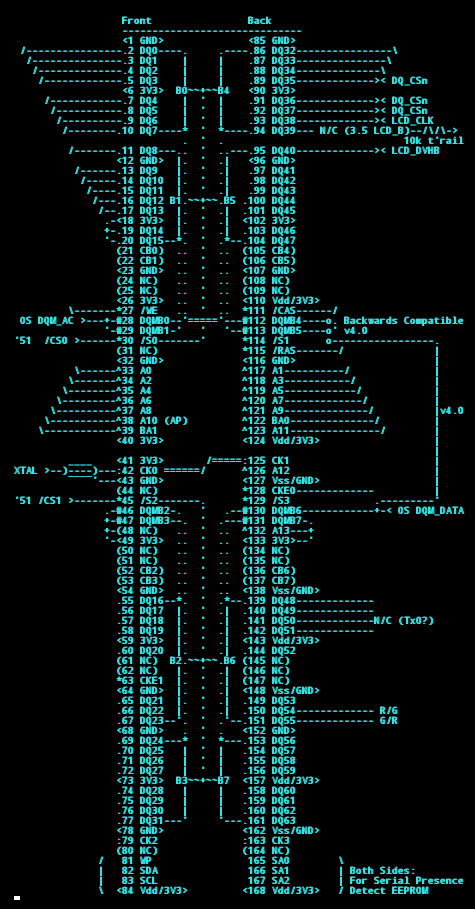
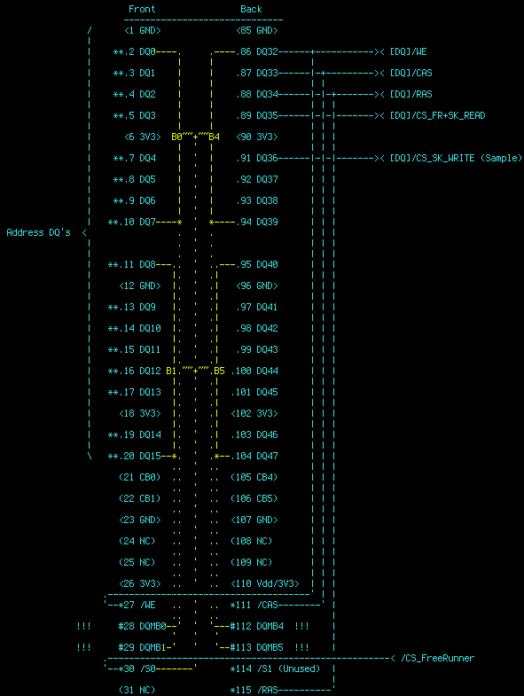
This is my pinout used in sdramThing3.0-4.5 Note the groupings of the Chip-Selects with their associated bytes. #sdramThing4.5 "Logic Analyzer" used an 8-chip single-sided DIMM. This first prototype for sdramThingZero will use a 4-chip single-sided DIMM (due to supplies), the Chip-Select->Byte-Mapping appears to match.
(Only look at this for the pinout/mapping of the DIMM... this is the *old* schematic... new schematics are in the following steps).
![]()
-
3Step 3
Plan your approach
For this early prototype, I plan to use a solderless-breadboard...
I won't be making use of all 32 bits that could be used for logic-analyzing... maybe just a handful for now, I don't feel like soldering *all those pins* for this proof-of-concept. (That's best left for a PCB!)
Looking again at the image, above, you can see there are still quite a few pins to be soldered-up...
So, how am I going to connect this thing to the breadboard?
Normal breadboard-wires are pretty heavy-duty, soldering them directly to the DIMM's pins will most-likely rip up the pins (aka "Pads") after a while. So, it's a good thing to consider.
I happen to have a bunch of thinner solid copper wire from old phone-wiring... This stuff works well in new breadboards, but old worn-out breadboards may not make a tight contact with these wires... So, again, think about what you've got to work with...
If anything's gonna fail first, it'll be at the connections!
-
4Step 4
Solder up them Address-Lines (And Clock)
The core-concept behind sdramThing is that of loading (half of) the memory-locations with commands that will be (eventually) directly fed-back to the SDRAM itself. Taking into account the characteristics of SDRAM, it's possible to wire those Address (and Command) pins *directly* to the Data pins. It takes a bit of software to make it work, but that's easier than a bunch of multipexers!
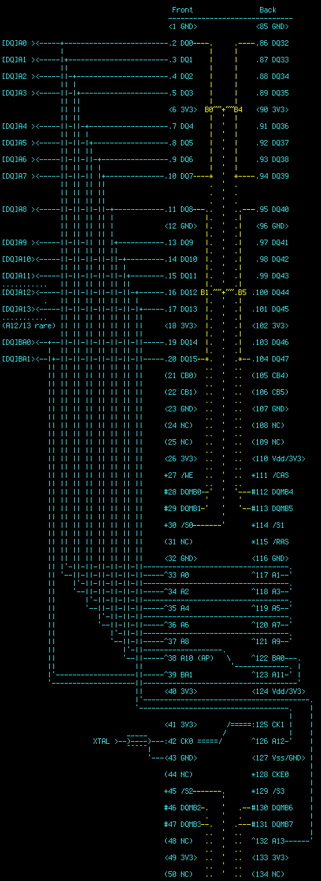
So, first things first, let's solder-up those Address (and Bank-Address) lines to the appropriate DQs (Data pins). And, be sure to leave a good few inches to connect to your breadboard!
(Yellow indicates the high-level/internal layout of the DIMM! E.G. Don't solder DQ0 to DQ7!)
![]()
(Note that A12 and A13 are rare... I have yet to run into a DIMM that uses 'em...)
Really, it doesn't matter *which* DQ's they're soldered to, as long as they're all on the same Chip-Select.(/S0, pin 30). But, YES, it *does* matter *which* Address-pins are which, so try to keep them in an easily-discernible order, to make breadboarding easier.
Pedantic: It's probably not highly-necessary for this low-speed (highly limited by the breadboard) prototype, but it's nice to keep the wires as equal-length as possible. The last time I did this, I cut all the wires the same length, then soldered 'em up. (I used "wire-wrapping" wire, 30AWG, last time, but that's *way* too small for breadboarding, so probably 30AWG between DIMM-pins, and something a bit thicker to go to the breadboard).
Pendantic 2.0: Yeahp... I'm leaving some DQ's floating... Yeahp, that's not a great idea... but it hasn't caused problems, so far... If you're really worried about it, wait until this whole thing comes together, then tie those remaining-floating DQ's to V+ via a pull-up resistor.
Advanced: I also make some effort to keep the fed-back Address/Command pins on as few Bytes as possible (B0, B1, B4, and B5). That way, it's possible to use one dedicated byte for other purposes... e.g. outputting a custom waveform... In which case, it's handy to have those particular signals on their own DQM, so they can be rewritten without modifying the "Free-Running" (Fed-Back) Commands.
Advanced 2.0: I'm contemplating using a (small) circular-buffer and an external trigger-input, allowing for a bit of "pre-trigger" data-storage. This could be done by e.g. using two separate DQs for A0, with a multiplexer inbetween. Prior to the trigger, it would cycle through a small portion of memory, overwriting old samples until the trigger's detected. Once-triggered, the mux would choose the second DQ for A0, causing the system to advance through the entire memory-array. FOR NOW, this is NYI. Things like this can be done elsewhere, as well... In fact, this technique is used for the Chip-Selects... But, I'll be keeping this initial prototype pretty simple. Though, it may be worthwhile to consider using wiring/soldering-techniques that allow for such modifications later down the line ;)
CLOCK:
Note that it's been found to be *quite* beneficial to *shield* the clock-wire... I used the wire leading up to an old WIFI antenna (found in an old laptop), but that may be a bit overkill... probably (shielded) headphone wire would be good 'nough.
And, yes, solder CK0 (pin 42) to CK1 (pin 125). This is a short-run, it doesn't need shielding.
-
5Step 5
Solder up them Command-Lines!
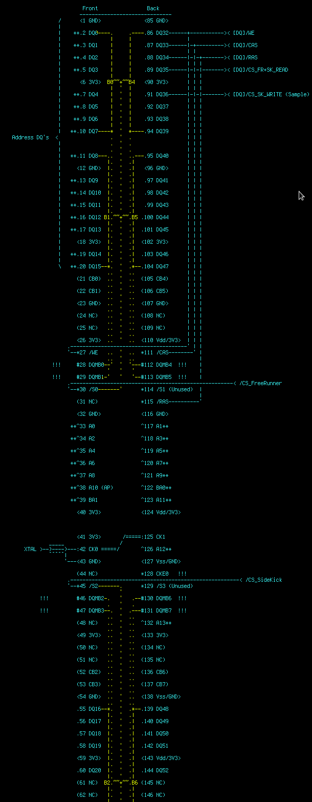
Similar to the Address-Lines, we have some Command-Signals which are directly wired to Data I/O's...
Note that when Chip-Select is inactive (/S0, /S1, /S2, /S3 is high), the command will be ignored by those connected SDRAM Chips.
Thus... We have two separate "units", the "Free-Runner" which outputs the commands, and the "Side-Kick" which--in the case of this logic-analyzer--samples the data and stores it in its memory-locations.
We'll store two separate sets of commands in the Free-Runner: those for the Free-Runner (READs-which causes it to continue outputting commands, sequentially), and those for the Side-Kick (WRITES-which causes the side-kick to sample data).![]()
Reading-back the sampled data from the Side-Kick will be handled by the host.
Advanced: Because the write and read latencies differ, the "READ" command can be stored in a different memory location than the "WRITE" command, and the two systems will remain synchronized.
Advanced 2.0: The side-kick needn't be limited to sampling data, it could also be used to output data (much like the "spare byte" mentioned previously). Thus, the Side-Kick's Chip-Select line isn't *directly* tied to the associated DQ. Instead, it will be fed through a multiplexer, which chooses whether the Side-Kick pays attention to the "Read" or the "Write" commands.
TODO: This was necessary in #sdramThing4.5 "Logic Analyzer" because it was a "sample/repeat" logic-analyzer. sdramThingZero, on the other hand, samples data once, then the "host" reads that data back into its own internal memory... byte-for-byte. So, is there any reason, really, to have a mux on the Side-Kick's Chip-Select...??? Hmmm... NOTE: directly-wiring the CS line to a DQ isn't doable, as doing-so will actually send a command to the SDRAM at the same time as attempting to load that SDRAM's DQs with a command that should be sent later. I think this MUX is a good idea, even if "repeat" isn't implemented.
-
6Step 6
Account for Esot-Fails (thus-far):
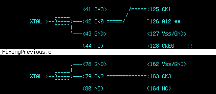
CLOCKS: CK2 (and CK3?) should also be wired-up to your crystal-oscillator... (Which'll be on the breadboard, later).
(Apparently my DIMMs, previously, didn't match the Intel Spec... Allegedly CK0 and CK2, pins 42 and 79, are supposed to be used for a single-sided DIMM. So rather'n try to figure out which CK# inputs are used by your chips--which could be done with a multimeter--you could just solder all the CK inputs. )
Recommended-course-of-action: have *two* shielded-cables running up to the DIMM for the clock-inputs.
![]()
These cables should be Pretty-Durn-Close to matched in length... I mean, a cm or so shouldn't matter, at breadboardable speeds, but don't be cutting one shorter than the other intentionally. This, frankly, goes for all the wires both between the breadboard and the DIMM as well as those fed-back on the DIMM itself...
NOTE: As it stands, I've been focussing on a single-sided DIMM. If you choose a double-sided DIMM, for now anyways, just expect that you'll only have *half* the available memory for your project... (That may be a simple modification, but is NYI... Something about adding additional Chip-Select DQs...?)
Advanced: If your DIMM has ECC (Rare, but possible...) you could have 40bits sampled simultaneously (rather'n 32)! BUT: Doing-so requires swapping the Free-Runner and the Side-Kick, due to the routing of the Chip-Selects... This is... NYI, and, further, would require (a little bit of) additional circuitry... If you want to try it, though, keep it in mind! Another possibility is using that extra byte on the Free-Runner, again, for additional waveform-outputs.
-
7Step 7
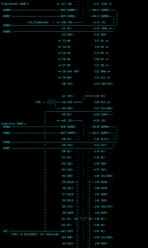
Solder Up that CKE and DQMBs!
CKE is the "Clock Enable" input, which is what makes sdramThingZero possible.
(In the #sdramThing4.5 "Logic Analyzer" era I was under the impression the only way it was possible for a "host" bus, running slower than the SDRAM, to write to/read from an exact memory location on SDRAM with directly-fed-back wiring was to have *exact* timing between the "host" and the SDRAM... which wouldn't be possible with most hosts' GPIOs. CKE should fix that requirement! making sdramThingZero possible. WEE!)
DDR? Sorry... DDR doesn't utilize CKE :/
DQMBs are the Data-Mask inputs. By utilizing these, we can choose *which* byte--of the 8 available on a 64-bit wide DIMM--is accessed, despite several chips' sharing a Chip-Select.
But even more importantly, we can control *when* a byte is accessed. This is important with the directly-fed-back wiring.
E.G. Say we want to write the value 0xff to Byte 4, at address 0...
(Below is a snippet from our wiring in an earlier instruction)
![]()
The problem is, the WRITE instruction has to be loaded to the CAS, RAS, and WE inputs. But, the "WRITE" instruction, when-commanded, loads the data on the DQs at that time (which are connected to CAS, RAS, and WE) into the memory-address selected. Instead of writing 0xff to Byte4 address 0, we'll be writing the WRITE instruction to Byte4 address 0!
So, then, how do we load 0xff to Byte 4?
- First, set DQMB4 so that Byte4 *ignores* the data on the DQs (the WRITE instruction)
- Start a WRITE BURST at, say, address 1013
- Load 0xff to Byte4's DQs
- Then 11 SDRAM-clock cycles later, the write-burst has now wrapped-around to address 0
- Unmask DQMB4 (for one SDRAM-clock cycle) so that 0xff is written to address 0.
You can see the *exact* timing necessary... the "host" has to know *exactly* when 11 SDRAM-clock cycles have occurred to unmask that DQMB at exactly the right address location. (And, it has to be fast enough to do-so!)
Utilizing CKE allows for a new "trick"...
Rather than starting the WRITE BURST at, say, address 1013, and waiting for 11 SDRAM-clock cycles, we can now start the burst at, say, address 1023, and wait as long we want to get around to unmasking the byte...
- First, set DQMB4 so that Byte4 *ignores* the data on the DQs (the WRITE instruction)
- Start a WRITE BURST at, say, address 1023
- Disable CKE on the clock-cycle immediately following the WRITE instruction
- The clock will now be ignored
- The burst will pause at address 0 (address 1023 would've been written at the time of the WRITE instruction, but of course DQMB)
- Twiddle your thumbs doing whatever you want... Got an LCD to update? Go for it!
- Load 0xff to Byte4's DQs
- Unmask DQMB4
- Strobe CKE for *one* clock-cycle.
Alright! Now you can have a linux system running keyboard interrupts and various other tasks, and still write the exact memory-location you wish to write, and even via a *really* slow GPIO port.
The only thing is, how do we strobe CKE for only one SDRAM clock-cycle when the bus is much slower than the SDRAM-clock? That's where the one-shots come in... More on them later.
Aaaaannnndddd... That explanation might be a bit much for this instruction, wherein you just need to solder up leads to the CKE and DQMB pins...
![]()
-
8Step 8
Final DIMM-Soldering (until next time!):
We're almost done soldering to the DIMM before we can get to breadboarding... There may be some modifications in the future, so don't seal the thing up in epoxy...
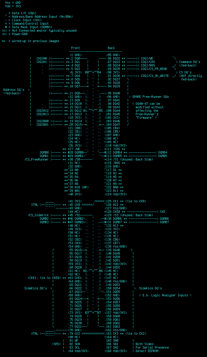
POWER: They're pretty clearly-marked on the diagrams... Solder up some hefty wires for 3.3V and GND... You don't have to solder *every* connector. In fact, I only used a 28AWG wire soldered to one point for 3.3V, in the last version. So, your breadboardable wire soldered to one pad (or maybe a capacitor?) is probably enough. (I also used two hefty/stiff wires--actually paperclips--as stands... soldered to ground-pads.) I also tacked an extra 22uF capacitor on-board... because: OCD.
(Oh, and, technically, I previously overdrove the thing with 3.6V... so maybe bigger wires connecting to a *few* pads would probably be better for 3.3V...)
SideKick DQ's: These are the bits that can be used for logic-analyzing. I'm tired of soldering, so I'll probably only solder up a handful, maybe one byte, for now. Later I'll probably solder up another byte, or maybe a few bits from each of the four bytes just to verify my circuitry before designing a PCB...
In #sdramThing4.5 "Logic Analyzer" I wired 2 bits from the Free-Runner, and 2 bits from the Side-Kick to the four signals on a laptop LCD (FPD-Link). I'd love to use that as an early-example, but it was based on a lot of prior-experimentation pushing the limits of that particular LCD, and used a lot of code to calculate a frame, Hsync/Vsync timings, and the simulated FPD-Link waveforms. Besides, sdramThingZero is aimed at being a logic-analyzer peripheral, so its side-kick is more meant to *sample* data, rather than *output* it. But, in case you're getting bogged-down in all the effort you've put in so far, here're a couple images of what's been accomplished with various previous versions of sdramThing, and sdramThingZero should prove even better:
![]() (This guy is displaying every possible color on a 6bit-per-color display...)
(This guy is displaying every possible color on a 6bit-per-color display...)![]()
(This guy is redisplaying the raw samples stored in the Side-Kick during logic-analyzer mode when connected to a fading LED. You can *barely* make out the blue "cursors" which are stored in the "extra byte" on the Free-Runner (the one with a separate DQM), alongside the Hsync/Vsync timing which is sent on the same wire as Blue. The FPD-Link Clock signal is stored in an extra bit on the same byte as the Free-Runner command-DQs. This is so that the LCD's clock signal needn't be rewritten every time the cursors are moved.)
So, with sdramThingZero we'll be sampling data into the Side-Kick--just like was done by the older system in the last image--but instead of designing the system around the intricate details of a particular LCD, we'll read that sampled-data back into our "host"'s memory to be displayed (and manipulated!) on a regular-ol' monitor with much nicer cursors and standard-looking timing-diagrams (or whatever you wish to do with the data).
Suffice to say, don't bother wiring up all 32 bits (or connecting an LCD), yet... We'll start with an LED or two, then move up from there :)
So, for now, solder up a couple wires to, say DQ48 and DQ49, to go to your breadboard... Maybe three if you want to analyze some SPI data or something. But, don't forget which DQMB is associated with whatever bits you choose!
Above is basically the entirety of the wires that should be dangling from the DIMM ready to be breadboarded... I hid the details of the fed-back pins, the chosen SideKick DQ's, and the Power. Don't forget those!![]()
At this point, the DIMM is ready to be breadboarded.
(And... I seem to be in the conceptual-phase right now, so it's entirely plausible you're farther-along in these instructions than I am.)
-
9Step 9
INSTRUCTIONS STATUS:
THIS IS WAY OUTDATED...
Hey, I need to revise these instructions a bit, per some changes I made during the actual process... So, if you've actually been building one of these, please let me know before I change it all up.
Instruction TODOs: (Everything hereafter should probably be in a LOG instead)...
Don't add the clocks until the end... they're bulky and get in the way.
(Using old shielded between-PCB wires from a VCR... this time).
Using a cropped-motherboard as a breakout...
A13 on the ol' mobo is actually grounded.
Mobo capacitors, remove all, start over. (Measured 1kohm between 3V3 and GND, turned out to be a dead ceramic cap(!))
Lengths...? Meh...
Free-Runner first, Side-Kick after
DIMM module Numbers
TODO: Keep in mind separate Buffer/Register circuits for testing for shorts-on-DIMMs (e.g. /CS).
Per a message, I've apparently not specified *which* SDRAM modules I've had luck with... and that prompted me to make this prototype a bit more versatile. Rather'n soldering directly to the DIMMs, as I'd done in all previous versions, this time I'm using a DIMM socket. I'll get it running and throw some info on the various modules in a list. As it stands, none of the modules used in previous prototypes actually have part-numbers besides the ICs' part-numbers, which are not particularly meaningful if the DIMM PCB manufacturer decided to spin a board that doesn't meet the standards... So, really, you need to use your multimeter and check the layout as per the previous instructions.
When this thing's a bit more established, it could probably test for those faults... I'll try to keep that in mind.
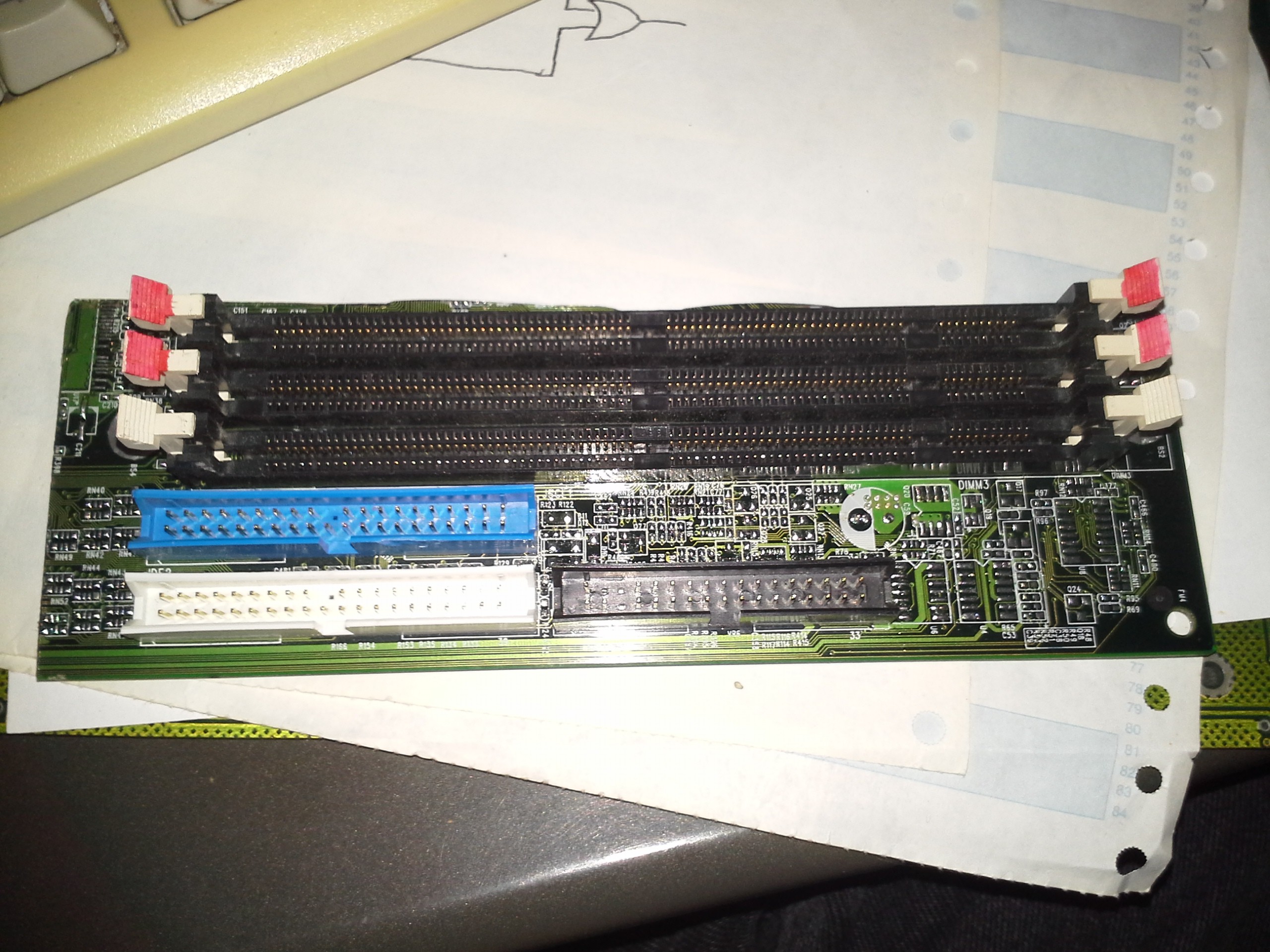
So, I cut up an old motherboard... It wasn't particularly easy to cut, so I was too lazy to cut off the IDE connectors... Turned out to be a benefit:
![]() With a bit of work, this old (fried!) motherboard's DIMM slots and IDE connectors are acting as a DIMM breakout-board.
With a bit of work, this old (fried!) motherboard's DIMM slots and IDE connectors are acting as a DIMM breakout-board. (more info at: https://hackaday.io/page/1299-repurposing-ide-cables-even-for-video)
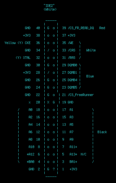
So far I've decided to only wire-up the free-runner (not the side-kick), as most of sdramThingZero's new functionality can be tested with only that (saving a bit of wiring, for now). And it just happens to be that the entirety of the Free-Runner's necessary pins can be broken-out to one IDE connector:
![]()
The only major change to sdramThingZero (vs. #sdramThing4.5 "Logic Analyzer") that might prevent its functioning is the use of CKE, as described earlier.
So, first-things-first, I plan to test that out... I can do that pretty easily with an old AVR -- the ATmega8515 has enough pins and happens to be in my collection.
So, I'll hold-off on whittling this down to the 8-bit data-bus I'd originally intended, as that'll require a few registers and buffers (possibly in the form of network resistors). It's still in the plans, but not necessary for testing CKE.
And, in fact, testing CKE can be done without a one-shot, as long as the SDRAM-Clock and the AVR-clock are identical. So two instructions in assembly for this test, vs. the 100 or so in sdramThing4.5... and *no assembly* once the one-shot is running.
So:
Tests TODO:
- AVR-CKE test will determine:
- Can we get away with only one one-shot, on CKE, or do we need 'em on the Chip-Selects as well (for other instructions e.g. "Load Mode Register")? (Documentation regarding use of CKE for most-anything other than pausing a data-burst or "power-down" (and what that means, really) is *sparse* to say the least).
- ...
- AVR/SDRAM on different clocks with one-shot(s) (just to make sure)
- At this point, could be driven by any "host" with enough GPIOs
- Buffers/Registers -> 8-bit bus (16? 32?) + a few control-signals
- At this point, could be driven by any "host" with at least 11ish GPIOs
- Yeahp, for some reason I'm still contemplating using a USB->Parallel adapter... stupid, maybe, but why not...?
- (Is there any benefit to reading the SPD...?)
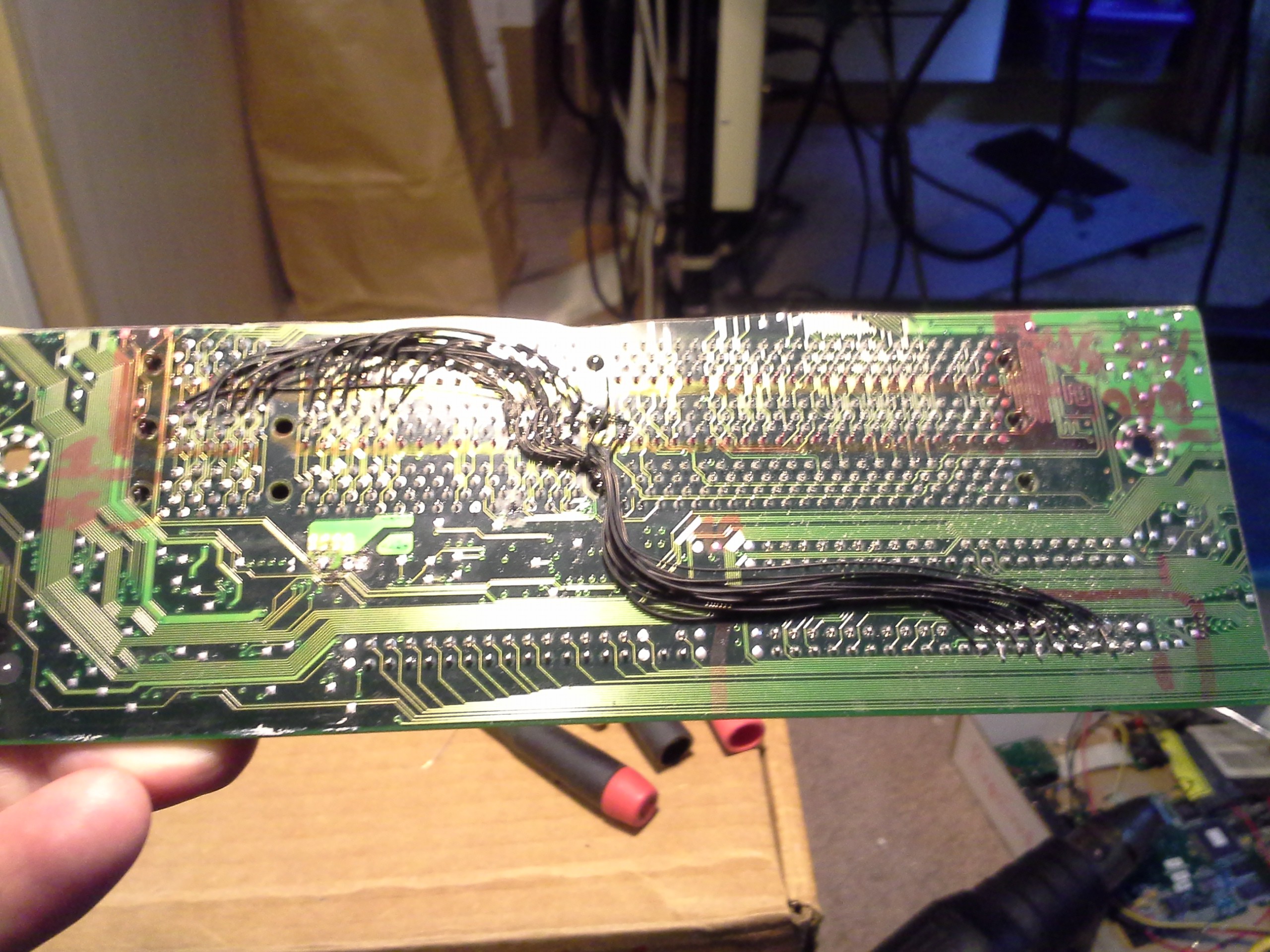
Didn't take many pictures... Here are the address lines and associated DQ's now routed to the IDE connector.
![]()
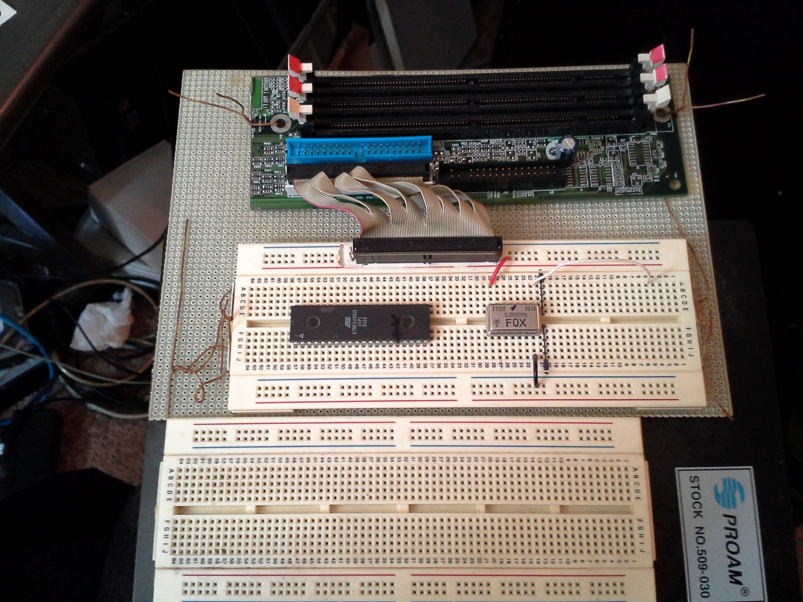
And here's my breadboard setup...
![]()
The short 80-wire IDE cable is from an old external USB->IDE case.
The breadboard with the 40-pin connector is something I built... oh... 15 years ago, for my Web-Controlled Robot (scroll down a bit). Originally it was a breakout for the 40-pin 8052 used in the robot. The 40-pin connector's signals are routed to the right on the breadboard... So the Crystal Oscillator is wired to the CLOCK input on the SDRAM. Handy that the 8052 and IDE just happen to have the same number of pins. Handier still that I built this thing so painstakingly all those years ago, and still have it available as darn-near the perfect tool for a completely unplanned purpose.
(Update: darned-near, but not quite. The (long) wiring is not shielded, unlike the 80-wire IDE cable... A better method would probably be something like #Breadboard adaptor for double-row pin headers)
So, it's been a good year(?!) now since I've done much AVR programming, may be a few days till I get my head back into that mode.
- AVR-CKE test will determine:
sdramThingZero - 133MS/s 32-bit Logic Analyzer
Add an old SDRAM DIMM to your SBC for a 133MS/s 32-bit Logic Analyzer, add ADCs for a Scope...
 Eric Hertz
 (This guy is displaying every possible color on a 6bit-per-color display...)
 With a bit of work, this old (fried!) motherboard's DIMM slots and IDE connectors are acting as a DIMM breakout-board.
Discussions
Become a Hackaday.io Member
Create an account to leave a comment. Already have an account? Log In.
Eric, you are the MASTER of ASCII art schematics. Wow. I'm wondering if some people might do better with a netlist? That would also tie nicely into making a PCB at some point in the future. Assuming a netlist could be imported to the PCB software... probably have to be edited, but at least it would provide a list of all the connections required. Or maybe that is a job for after the first prototype is running? E.g. go back and trace all the wires and figure out exactly what netlist ended up working.
Are you sure? yes | no
Thanks for the compliment :)
Netlists are definitely in the future!
(Un?)Fortunately, just discovered the 74x16543, which I'm mulling over whether it's worth it to "do-right" with, or to stick to my original plan of 74x574's and network-resistors (making use of the inherent latch/OE's already built into the SDRAMs during the read-back process). So, yahknow, netlists aren't yet set in stone.
Are you sure? yes | no
right... maybe after the prototype.
Do all the SDRAMS have that latch/OE? If so, the only drawback is increased current draw from the resisters, right?
Are you sure? yes | no
Indeed, good thought-point, that current-draw. There's also some risk of speed-slow-down, as the various pins' input-capacitances need to be overcome. There's a new "log" on my perceived pros-and-cons... would be interested to know your thoughts.
But, yeah, prototype, dammit, prototype! In this current time-period I might even get away with even the 1980's 5V-7400-series (and LS, S, F, and A!) chips in my collection... I've had surprising luck running 'em at 3.6V!
Oh, yeah, SDRAMs' latch/OE functionality is inherent to the standard... So adding an additional latch with OE is a bit redundant. Not *bad*, but kinda defeats showing just how much they're capable of on their own.
-----
And now... some vague/slightly-drunken perception that many of those latches' necessity might be removed by a "bootloader" and even more fed-back pins... This is *really* vague.... hmmmm
Are you sure? yes | no