And best part for the last, if you look on the last image regarding project you will find one bread/protoboard that is connected to ChipKIT MCU dev.board and then via USB to SoC.
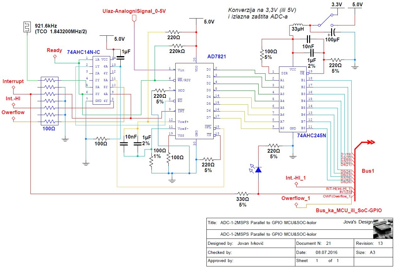
What you can not see is that it is fast -flash 8bit parallel ADC based on 1-1,5MSPS AD7821 IC.

It is interesting to point out that this ADC was stable at 1.5MSPS and that on that speed 8-bit Atmega 328's (Arduino Uno/Nano) was to slow to read and merge 2 binary ports. Arduino Due with Atmel SAM3 end up slower then ChipKIT's PIC32mx250 MCU on the task. But winner was by no surprise Raspberry Pi3 that without much problem blink and read any GPIO port faster than ~55MHz.
 Jovan
Jovan
Discussions
Become a Hackaday.io Member
Create an account to leave a comment. Already have an account? Log In.
OK, I accept all of your elaborated reasons, but how dose you explain that it is WORKING.
IT is also worked in 74HC245 version but I opted for faster IC with greater fan-out.
I can send you pic's and oscilograph to show that SN74AC245 work on 3.3V Vcc and translate TTL input to 3.3V.
Are you sure? yes | no
It is working but you don't see the actual details going on when you have a '1' on your ADC with a high bandwidth scope with a good active probe.
The ADC would drive the pin high, causing the diode at the buffer to conduct. This will be a short burst of over current. This extra current *could* affect your ADC SNR and over time the reliability of your buffer circuit. Have you look at the noise floor on your SNR and ENB using a FFT?
All I can say is that I have spent a lot of time working with signal integrity, level conversion, and working with designing reliable systems and even did some data acquisition work back in the days on my thesis and a product, so I know what I am talking about.
tl;dr Yes, it works, but you don't know you had a bad design. Still in the denial phase I see.
You are free to do whatever you want with your design.
I really don't care much about this project just pointing out what I can see wrong within that first 15 seconds of seeing it, so you can save your time etc no need to convince me otherwise.
Are you sure? yes | no
I really thank you for your time, interest and elaborated insight. I also highly appreciate all your suggestions, as I already use one 74AHC IC in circuit and I do not see problem to unify design and use two of them as you suggested.
Now I will take some of your time to elaborate my point of view. 74AC series is 5V tolerant without any doubt but with limitation that I was/am aware of, that 74AC IC have recommendation not to be used for over Vi = Vcc+0.5 V. In my practical implementation after using 74HC series, 74AC245 end up as fully useful and functional and in excellent shape for task of converting nominal TTL 5V input to 3.3V CMOS. But here's the catch that makes the difference between theory and practice, if look at AD7821 (and AD7822) datasheet you will find that Logic output level for VOH = 4V max and Iout = 3uA (74AC limits of Input Diode Current is 20mA) and in real use VOH is ~3.7-3.8V and Vcc=3.42V, and you will agree that is fully within 74AC245 specs. I understand that it "strikes the eye", but theory and practice can be real different (if we do not know all the facts). Any way that 74x245 is just support element as unidirectional non-inverting buffers, for 5V TTL level not tolerant Arduino Due and Raspberry Pi and as such it already took to much of our time.
Best regards,
Are you sure? yes | no
Hi Lee, we can start long debate over datasheets but lets skip it at start.
74AC series operates in 2-6 V range and it is 5V input tolerant (0 - Vcc) .
It also have advantage, like 4x bigger outputs source/sink current of 24mA than AHCs (8mA).
Any way I make that curcut and it work flowless on RoPi 3.3V GPIOs.
Check this:
http://www.ti.com/product/SN74AC245
Thank you for interest ;)
Are you sure? yes | no
Incorrect! If you actually *understand* the datasheet and the differences of logic families.
Under "Absolute Maximum Ratings" for 74AC series:
DC Input Voltage (VI) −0.5V to VCC + 0.5V
This basically means that there is a protection diode going from the input to VCC rail. This makes it non-5V tolerant if running from a 3.3V source. i.e. Input is only up to 3.7V for a 3.3V supply.
"it is 5V input tolerant (0 - Vcc) " This is where you are mistaken. If Vcc = 5V, then the part can accept 5V input, which means now the output then will also be 5V. Your switch shows it has VCC= 3.3V selected.
For a 5V tolerant part e.g. 74AHC
VI input voltage −0.5 +7.0 V
This basically means that the input structure has been modified to allow for input to exceed Vcc.
Are you sure? yes | no
74AC245 when running at 3.3V is not 5V tolerant. You want something like 74AHC245, 74LCX245 etc for 5V to 3.3V level shifting.
http://www.nxp.com/documents/data_sheet/74AHC_AHCT245.pdf
Are you sure? yes | no