 Nixie
NixieSo, while waiting for the turbopump to arrive, my mind was left meandering around, and thinking about the PMMA masking, and the difficulty to obtain very low molecular weight masking liquid...
I thought...
If Silicon is sort of transparent to 10600nm laser light...but PMMA is not...can't I just use laser etching to patern low resolution features on my test wafers?
With that thought, I prepared a test vector file with lines separated 100µm - 200µm - 300µm for the laser cutter:
After lasing that, I mcgyvered this microscope to see the tiny details:

And here's what I saw:
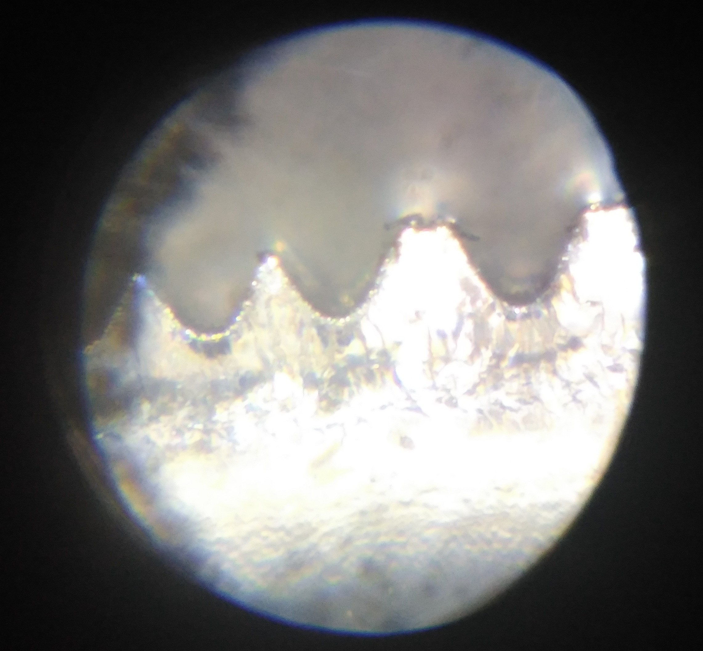
The trench etch looks fairly constant:

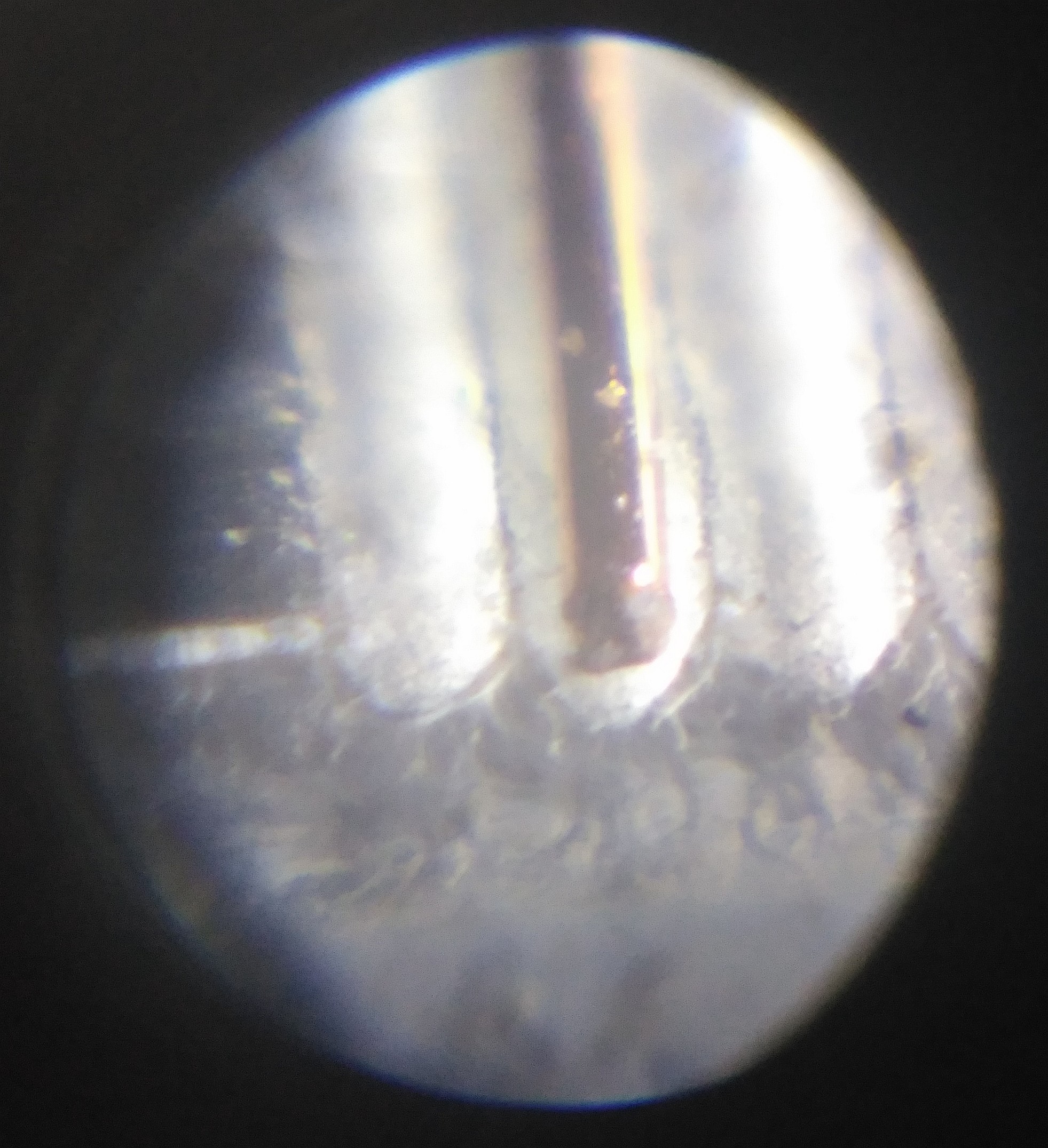
a 110µm copper wire for scale:
The plan is as follows:
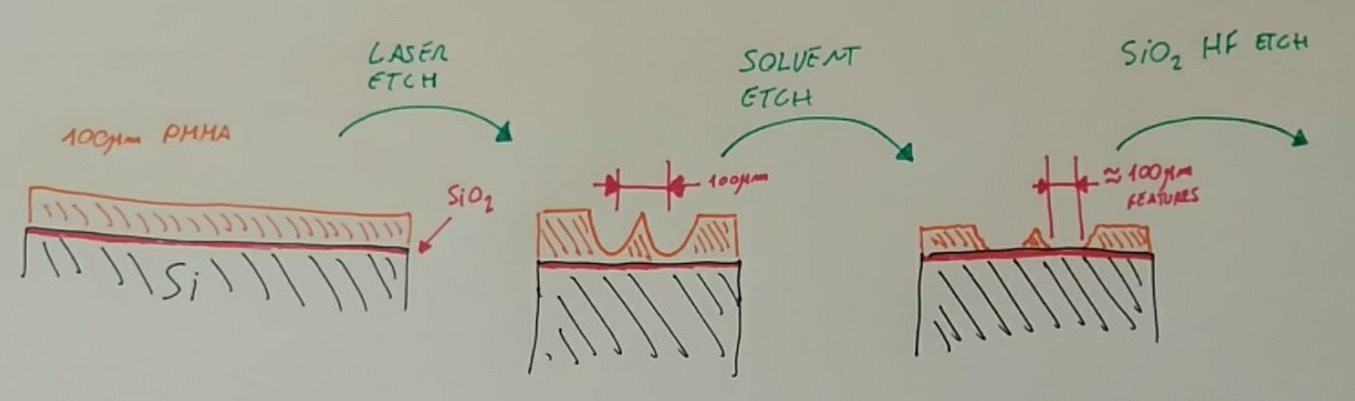
You first etch the PMMA with the laser, but not trying to go all the way, just to the top of the silicon wafer. Then, using PMMA solvant, you eat away some thickness from the leftover PMMA, revealing the silicon on the bottom of the trenches.
After that, an anneal step and you can etch the wafer. This should enable 100µm features, with 100µm spacing.
Wich frankly, is a really good start for me.
Discussions
Become a Hackaday.io Member
Create an account to leave a comment. Already have an account? Log In.