-
BF862 is now End Of Life. Well that sucks.
09/04/2018 at 13:41 • 2 commentsNXP has restructured, spinning off standard products into a new company called Nexperia. The BF862, beloved of physics projects, fiber optic bootstrap circuits and seemingly a particular favorite of WInfield Hill ("Art of Electronics") is not going along for the ride. Some LHC preamp projects report a resolution of better than 1kev in Ge with a room temperature BF862 so this is/was a pretty good JFET even if it was only intended for the preamps of car radios.
The important thing of course is not to panic.
So after panic buying the next logical step is to look back and assess the situation. In 2013 the people on diyaudio became concerned that the noise knee had increased when stated production moved to china. Some information came from the company that the chips were being fabbed in the same place and only the encapsulation point had changed. This seems unresolved. It's quite a difficult test to do and the small number tested may not be representative. Could dielectric noise be a contributing factor? That would potentially be affected by a change in encapsulation.
Possible replacements suggested on usenet by Phil Hobbs; On Semi CPH3910. Lower capacitance but higher Idss and NSVJ2394.
For my purposes the BF862 was a little high in input capacitance and I spent some time chasing Sony 2SK152's (which I found in all Idss grades except -1) and 2SK300 (which so far I have failed to find in any grade). These have 6 to 7 pf input capacitance versus the BF862's 10pf. In the same way the BF862 bulk application was car radio preamps the 2SK152 was originally produced for the head amplifier circuit of the Betamax video recorder and found it's way into shortwave sets and the Amptek X-ray spectroscopy literature where is performs the best of all JFETs tested except for a narrow low capacitance range where it's just beaten by the Interfet "NJ14". There are Interfet NJ14AL process JFETs, which may or may not be the same, available on mouser as the IF140, IF140A and IF142, but they are expensive. They may be worth matching with low capacitance detectors if MMBF4416 (related, cheap, low capacitance JFET) designs do well.
-
Op amps.
07/09/2016 at 23:31 • 0 commentsBeing able to measure a few thousand electrons accurately means using the best parts for the job but it starts with picking the right technology. While many applications are agnostic to the underlying design of the op amp they use I am of the opinion that the only way to build a preamp is with an FET input stage; That mean using an FET input op amp or a discrete FET input stage to an op amp. BJT and MOSFET inputs have the advantage of lower voltage noise (BJT) and lower current noise (MOSFET) but the low input impedence of BJTs and the high voltage noise of MOSFETs seems to pretty much rule them out for anything that can be built at home. High performance CMOS IC preamps have been designed in the literature but I see no way to apply this and let me honest here, I don't understand how they do what they do.
LMP7721
The elephant in the room in that the voltage noise and input impedance specs are awesome. It's used by the radiation watch project and Peter's OpenCT2. With femtoamp input bias currents this should be the obvious choice. Nowhere in the datasheet can I find mention of an FET input stage, so I think the high input impedance is down to the internal compensation. This is doubtless a really good solution for pH electrodes and other slow ultra high impedance sources but the window between voltage and current noise for success in this project is narrow. The current noise for this op amp is around 100 times higher than I'd expect for an FET input and maybe tens of thousands of times higher than if it were dominated by the input current. The other thing to note is that while this chip has femtoamp bias currents the best sensors I'm looking at have hundreds of picoamps of leakage current which means replacing a 10 picoamp op amp with a 10 femtoamp op amp is of questionable value. I will certainly need to test one at some point to be sure but I'm ignoring it for now. About 5 USD.
MAX4475
It's the application note for the 4475 that started hobbyists using PIN diodes as replacements for Geiger tubes. On looking through the specs, this seems to be a pretty good candidate for spectroscopy but I've yet to see anyone use it this way. About 1 to 2 USD.
MAX4488
A 4475 without the feedback compensation. Higher bandwidth, higher slew rate, not unity gain stable. Might be ideal for the preamp. Might work well in parts of the shaper, but there really isn't a requirement for an FET input amplifier for the shaper. The 4475 and 4488 are where I'm pinning my hopes at the less expensive end of the design. About 1 USD.
TL082
The first version of the freshlab circuit uses this dirt cheap op amp for the preamp and the shaper. Higher noise and higher slew rate than the 4475. That circuit performs badly, but I'd be an idiot not to replicate it as a benchmark. Will the lower noise but lower slew rate 4475 be better or worse, and how the hell does a chip with such low bandwidth have such a high slew rate? Large variation in price but some under 15 cents.
AD8012
Low noise, not FET input. This was used by the shapers in 2 or 3 documented projects (depending on if you take the 8011 to be equivalent) but circuit diagrams are not available. As a current feedback op amp they are difficult to design for. With a discrete FET this could work for a preamp. I felt this was my best option for the final design a few month s ago but difficulties in using them and questions over effects of current noise in the negative input have left me with doubts. For now these will be staying in the box. Approx 2-3 USD.
OPA657
Low noise, low input capacitance, insane >1GHz gain bandwidth product, ideal and proven as part of a preamp (the freshlab high performance design used one). The only disappointing thing about this is the price (circa 10USD) which isn't so high as to exclude it but isn't so low as I can grab a bucketful and use it for every function in every prototype. I am hoping for better performance using a discrete low noise FET and a cheaper op amp. Both using the 657 and attempting to beat it are going to have to wait.
There are cavernous pit falls in trying to match spec sheet values to applications. Ultimately it must come to down to real tests, but I've done what I can to select good candidates and to keep the search space for the final design manageable.
-
Progress (lack of). Excuses etc.
07/09/2016 at 22:20 • 0 commentsIt's to my shame that at a time when I want to devote my full attention to a project that 3 more important things come along. The car at the top of the road that rolled down and largely destroyed the front wall of the garden about three weeks ago and the small tree falling over onto next doors fence and ripping the wires out of my satellite dish which happened yesterday don't even figure in the 3. Only the British sense of irony is audacious enough to suppose that for their own amusement the Greek gods are playing chess with our shrubberies.
If I'd been more organised, more focused, worked smarter not harder I'm sure I'd have much more done with the same free time, but that would need someone who isn't me.
The big chunks of metal that needed to arrive have. A shaping amplifier to test the preamps with and a NIM bin (glorified power supply) along with a few bits and pieces I should have bought years ago like a temperature controlled soldering iron. A flurry of components for the 2 cheaper versions of the preamps and the very clever forward biased design were also rapidly ordered and have arrived. I forgot to order any metal project boxes, so light and EM shielding are about to be a problem. Getting the shaping amplifier turned out to be more eventful than usual when the the parcel company that picked up the package from the plane put their stickers on top of the address and then couldn't work out who to sent it to. That isn't one of the 3 either. The amplifier is a little less flexible than I wanted, when buying off ebay I failed to notice the difference between shaping time and peaking time, but it's probably still the best from what was available and since I'll be replacing that with an open source design anyway it shouldn't matter.
One potential mistake is that when choosing the package for the max op amps I went for the 6 pin version thinking it would be easier to solder than the 8 pin version not realising that the 6 pins were SOT23-6's and rather smaller than a SOIC-8. Since I can't get the board design finished, exposed and etched before the July 11 deadline, in 19mins as I finish this log, I may simply order the SOICs and use the SOTs when I have a professionally made PCB.
There is currently no github for the design, but when I have some trial designs fit to be etched that is where they will go. I'll also need to finalise an open source licence. Right now I need to put together the parts I have in lots of different ways and see what combination works and works best, then I can move forward.
-
Existing attempts by others
05/30/2016 at 13:59 • 0 commentsI've tried to read everything I can find about other peoples attempts to do X-ray/Gamma spectroscopy with diode detectors in the hope of building on them and avoiding any pitfalls they found in the process. Clearly this is going to make me sound high handed and a jerk but there is very little firm ground to stand on.
http://freshlab.org/detektor/?lang=eng
This work is really inspiring. When I first saw this page in about 2011 it changed my view about silicon detectors and what it might be possible to do at home. The claim they've made in some descriptions of the circuit is a complete spectrometer for 20 euros. This isn't that. They made a preamplifier and a shaper and then attached them to what looks like tens of thousands of dollars of back end equipment. There is a version in English and Polish, they both describe the construction of the same circuit and the results are completely different. After spending a lot of time reading through everything I could find on this project it seems they built more than one version. Neither has a full circuit diagram, but enough information is given to put together the first low performance version after pixel peeping details from the photos and the simple but more expensive high performance preamp is documented well.
http://einstlab.web.fc2.com/Gamma/spectroscopy.htmlFantastic dedicated attempt. This is amazingly documented, the theory is spot on, great presentation and everything my project aspires to be except that it appears not to work. I am a little confused by his shaper chain, but the issue is that he has misunderstood what is possible with the X100-7 sensor. Frustratingly he also seems to understand the physics behind the sensor but he is pointing to and labeling shapes in the noise that may or may not be real.
Second version of a radiation meter published in Elektor which has very strange looking results.
-
Design and PCB plan
05/29/2016 at 19:36 • 0 commentsIn order to get decent performance I plan to build and then tweak several preamp and shaper designs. Some of these are simple and obvious but may need high quality components, some are very clever by the best in the field that publish and some will be crayon drawings by myself that lean on more expensive parts. The goal is to look at the trade off for the final design, performance versus cost.
At it's current state of development this project is probably a best fit for "Citizen science". I was hoping to have a proper shot at "Anything goes" but although I've read a lot, ordered some parts, daydreamed and dug out long forgotten priceless junk, I've so far accomplished nothing. Even putting some ongoing IRL issues aside I'm disappointed. In order to have any chance of being noticed by anyone, either to progress or just interested hackers, I feel I need to make very substantial progress by July 11th.
This must shape my plan. I don't have the time to evolve a design by international post and I don't need 10 copies of the same PCB to throw away the moment I have to make major track changes. Local small order PCB manufacturers work out many fold more expensive. I also need a large number of different simple circuits that with the addition of a few bus bars and copper foil shields would probably fit pretty well on a single side. I've dug out my UV exposure box and after 10 years gap hope to remember enough to do more than stain my fingers.
The plan right now is,
1. Fab preamp PCBs and test these with a second hand commercial shaper. The main advantage is that the shaping time can be changed over 2 orders of magnitude at the turn of a switch. The home made version will be much less flexible.
Fab the shaper op amp circuits at the same time. AD8012 may be a poor choice, the spec on paper is superb but being a current feedback amplifier brings a set of golden handcuffs and a mean attitude to the party. In addition Analog does not seem to be marketing the double CFB AD8012 among it's op amp line, even though the (slightly better specced) single CFB AD8011 is. I also worry that even though these should be fast and low noise that the preamp circuits are used for speed at the expense of energy resolution.
So also use a conventional design slow VFB op amp shaper. I'm wondering if a preamp with a slow op amp might be a better source for this circuit. CR-RC shaper may be fine and extra SNR can probably be recovered with processing. Probably best implemented as Differentiate-Amplify-Integrate (This is more a note to myself and will expand on it later).
2. With a working preamp and commercial shaper write the STM32 code to do Pulse Height Analysis that is the raw data for detection. Tweak for performance if needed. Test combinations. Abandon and move to an op amp based Wilkinson converter if the STM32 internal ADC isn't up to the job.
3. With a working preamp and home made shaper put everything together. Tweak. If the design had to move to a Wilkinson converter then pulse processing code is not possible and we need to move to a better shaper like CR-(RC)4.
-
Preamp
05/29/2016 at 14:11 • 0 commentsThe output from the sensor is a pulse of charge. The height, length and shape of the pulse don't matter much, only the total charge. So what is needed is a charge sensitive (integrating) amplifier.
Take a perfect amplifier with a large negative gain and place a perfect capacitor between the input and output terminals. Any charge placed on the input will generate an EMF and will immediately result in the opposite EMF being applied to the other side of the capacitor sucking the charge into it. Indeed the capacitance seen by the input is much larger than the component value by the Miller effect. This makes the input of the charge amplifier a virtual ground even though there is no DC feedback.
Translating this into a real circuit means working round one problem. Every time a pulse of charge enters the perfect circuit the output voltage steps up. With no way to discharge the capacitor any real amplifier will eventually saturate. There are two ways to solve this; Continuously discharge the feedback capacitor with a longer time constant than the pulses of charge to be measured or periodically discharge it before it reaches too high a level. The former is the easiest to do and can amount to as little as a high value resistor in parallel. The latter has the lowest noise but is more complicated.
So far, nothing scary. What makes this tricky to design and build is that the charge produced by a PIN diode is very small. A 5kev X-ray from a silicon sensor produces a pulse of less than 1400 electrons. To achieve 2kev resolution will requirea pre-amplifier with an input referred noise of less than about 220 electrons RMS. This means a good design, components and EMF shielding.
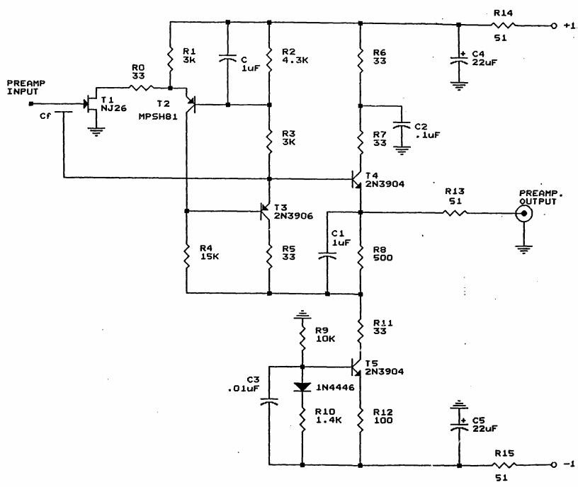
![]()
The Bertuccio1992 design is very clever and breaks previously established methods in nuclear electronics. For one the input FET is forward biased from the detector which is normally a nutty thing to do. The Interfet NJ26 is equivalent to the old 2N4116, low noise, low gain, small input capacitance. This is key to how they pull of the trick. A modern higher gain FET matching a larger input capacitance will likely burn out in the same circuit. It is probably unsuitable for detectors more than a few pf and it may need protection from nA level input currents. The rail voltages were not lost when I cropped the image, they are missing from the scanned sheet. I will chase. This is an awesome hack, but it's someone else's awesome hack and I will test a lot of other designs. It may be that modern op amps and FETs will close the gap.
-
PIN diode
04/26/2016 at 13:05 • 0 commentsThe main methods of detecting radiation are by charge separation or light emission. For a semiconductor detector we want a volume without charge carriers. When ionising radiation (the clue is in the name) is absorbed by this volume it generates electron hole pairs. If all the energy of the particle/photon has been absorbed then the amount of charge produced tells us something about the energy it had. Rather than explain everything verbose, here is what Wikipedia has to say,
https://en.wikipedia.org/wiki/Semiconductor_detector
Practically while we are only interested in a non conducting region, all semiconducting detectors are fabricated like a diode. Why a diode? Simply putting electrodes on a poor conductor produces a flow of charge, new charge carriers flow from the wires and the current maintains. By doping the ends of the detector and reverse biasing it, charges are swept out of the insulating region and new (against the bulk region) charge carriers that go in from the wires are mostly eaten by the majority carriers before they can enter the insulating region - this is diode action. Making it into a diode makes the insulating region perform much better.
There are commercial devices that fit this description - PIN diodes. While PN diodes generally have an insulating (depleted) region that is really too thin to be useful as a radiation detector. PIN diodes are fabricated to have an insulating region often as wide as 0.1mm and some as much as 0.3mm. In terms of physics this can't compete with the millimetre or centimetre thickness of cryogenic detectors, but in parallel with the development of the big boys there is always a need for cheap detectors with lower performance and there is about 45 years of relevant material behind subscription walls of major physics journals.
Selecting a good PIN photodiode for this application is probably impossible from the datasheet, but potential candidates for testing would have low capacitance (a few tens of pf maximum at high reverse voltage) low dark current (I don't know what is acceptable here but certainly no more than a few nA) at high reverse voltage and a wide depletion region (more than 50um is probably enough for spectroscopy).
Depletion width rarely appears on datasheets for optical PIN diodes, but there is a trick. The P and N regions of the device are essentially conductors, and the I region is an insulator so it's possible to estimate the depletion width as a parallel plate capacitor. Knowing the area of the diode and the capacitance of the junction for a given reverse bias (curve in the datasheet) and knowing the permittivity of silicon tells us the depletion width. My rule of thumb is that a PIN diode of 1 pf per square mm has a depletion depth of about 100um, so 2 pf would be 50um and half a pf would be 200um. This approximation works really well on large diodes 10 or 100 square millimetres, but is unhelpful for much smaller.
Breakdown voltage tends to scale with depletion width but this is not that reliable and also related to other aspects of the design and manufacture. 80 or 100um diodes tend to be rated for 30V or less, a 300um diode tends to be above 100V.
The two cheapest diodes I'm planning to try are the BPW34 and SFH206K, under 1 USD each, both around 7 square millimetres, 8 or 9 pf and a dark current in single digit nA. The BPW34 is the go to diode for most people in the hacker community wanting to measure radiation with a semiconductor, it's in the radiation watch project and in the excellent OpenCT2 by Peter Jansen, who is also solving the X-ray licencing problem by using a low level exempt radioisotope source. Science lit suggests the depletion width for this diode is around 150um, but that does not match the estimate. The SFH206K in science lit is stated to have a depletion width around 70um which matches the estimate well, maybe they used the same math. This diode is potentially less sensitive to radiation but no one doing X-ray spectroscopy has ever stated they had better results from the BPW34, the few times they have been tested side by side it's always worse. There are multiple manufacturers for the BPW34 and some specs are slightly different, this may complicate things. Removing some or all of the encapsulating plastic may be helpful and I'm not sure the best way yet.
I'm looking at a wider range of PIN photo diodes, some of the most promising candidates for resolution are intended for fibre optic use, these tend to be smaller and run at higher reverse voltages. The OPF420 is around 12 USD, has been used for X-ray spectroscopy with good results. The science lit is mixed on the depletion depth with one source claiming 300um and another 150um. This is in a metal can and removing the window 'should' be easy.
If any single manufacturer has a good reputation for photo diodes that can be used for X-ray applications, it's Hamamatsu Photonics. Among others the S1223 (20-30 USD) and S5821-02 (10 USD) have come up and coupling the the former diode sans window to an Am-241 source is one manufacturers party trick for calibrating the gain and measuring the noise of their commercial charge sensitive preamps. Hamamatsu used to sell direct from their website with a shopping cart, but not any longer. I have a reference to S5821-02 being the best diode and it's cheaper but I cannot find it for sale apart from RS Components, and they are only selling them in Japan. I may try contacting Hamamatsu and see if they will deal with me direct. To make things worse the paper describing how this diode is used to get the spectacular results I've seen is proving elusive. Farnell and probably others sell the S1223 and I will almost certainly test this diode to see if it's worth the extra money.
The elephant in the room is the X100 from First Sensor. Commercially available for around 100 USD and intended for X-ray/gamma ray use, including a visible light barrier. Robert Hart is using this in his Solid State Ionising Radiation Detector which has recently seen some renewed activity.
This is a big chunk of silicon and for a silicon sensor works very well for detecting radiation but my hunch is it won't work so well for spectroscopy. Robert bought sensors direct from First and paid less than the reseller rate but my current thoughts are this is too much of a risk and too expensive. I'm calling it outside the scope of this project.
Aside from low sensitivity at higher energies there are some drawbacks to commercial Si PIN diodes for X-ray spectroscopy, but these are minor and for the most part this long established physics hack punches well above it's weight. Anyone with a need for better performance needs 3 orders of magnitude more money just to buy the sensor. Most people using this hack are coupling them to commercial preamps and from those to expensive hardware. A few people who made their own preamps are telling people how and my next brain dump is about that.