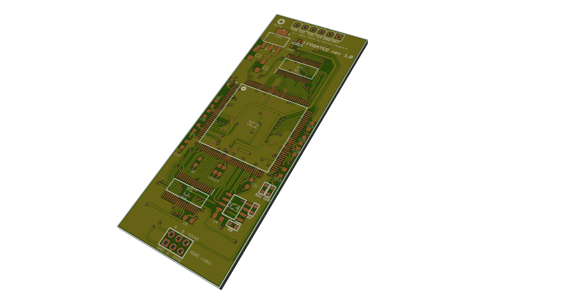
FPGATED hardware prototype is now in the finish!
The schematic and board layout was finalized, ready for PCB manufacturing.

This is hardware revision 1.0 using a TQFP144 Spartan6 FPGA. It is only a 2 layers PCB so most probably rev 1.0 is not the final production one. The main goal is to test all functionality in a C16 or Plus4 and then shrink it even further.
The production version will use a smaller BGA package FPGA with 4 layers PCB and cheaper IC socket connector. This one features an SMT mounting socket connector at the back in order make space for the TQFP144 on the top. Good news is that I have managed to route the RGBS signals to a small 2x6 connector on the top, so besides composite, RGB video signal will be available too.
I am now sourcing components but 2 items on the list has a bit longer lead times than I expected, so expect it running in Q1 2021!
Stay tuned!
 István Hegedűs
Discussions
Become a Hackaday.io Member
Create an account to leave a comment. Already have an account? Log In.
Not visible but on the other side of the PCB I am using an SMD 48 pin IC header. This component will arrive late february. I have now one prototype working with workaround IC header. I will post information on this site with pictures soon.
Are you sure? yes | no
Very cool that you're doing this!
Just curious, what are the "long lead time" components?
Are you sure? yes | no