Hi,
Heading into 2021 here is an awesome news for those who are waiting this moment for 4 years now! I have managed to build the first prototype of the FPGATED IC which is a direct drop-in replacement of MOS 8360R2 IC.
Here you can see how the empty and populated PCBs look like on the top.
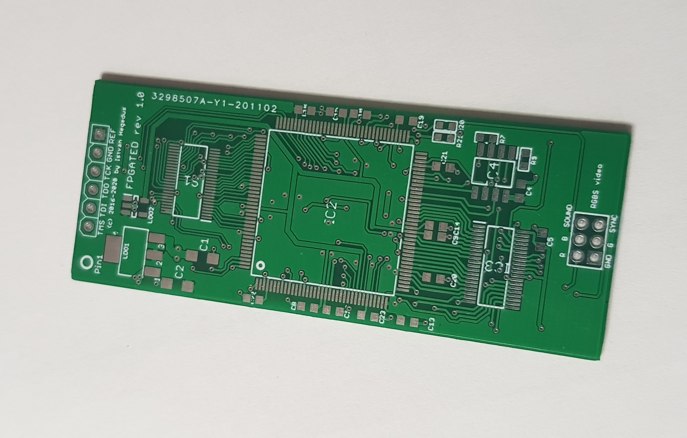 |
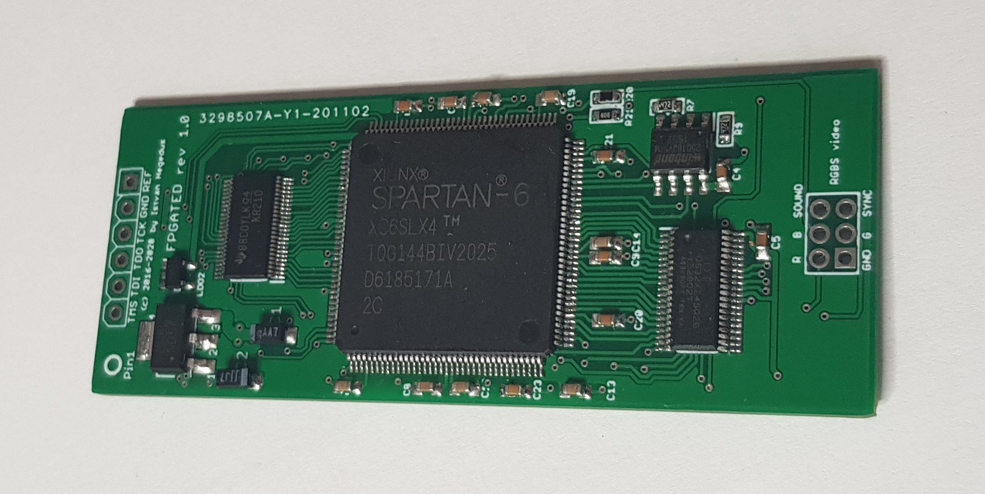 |
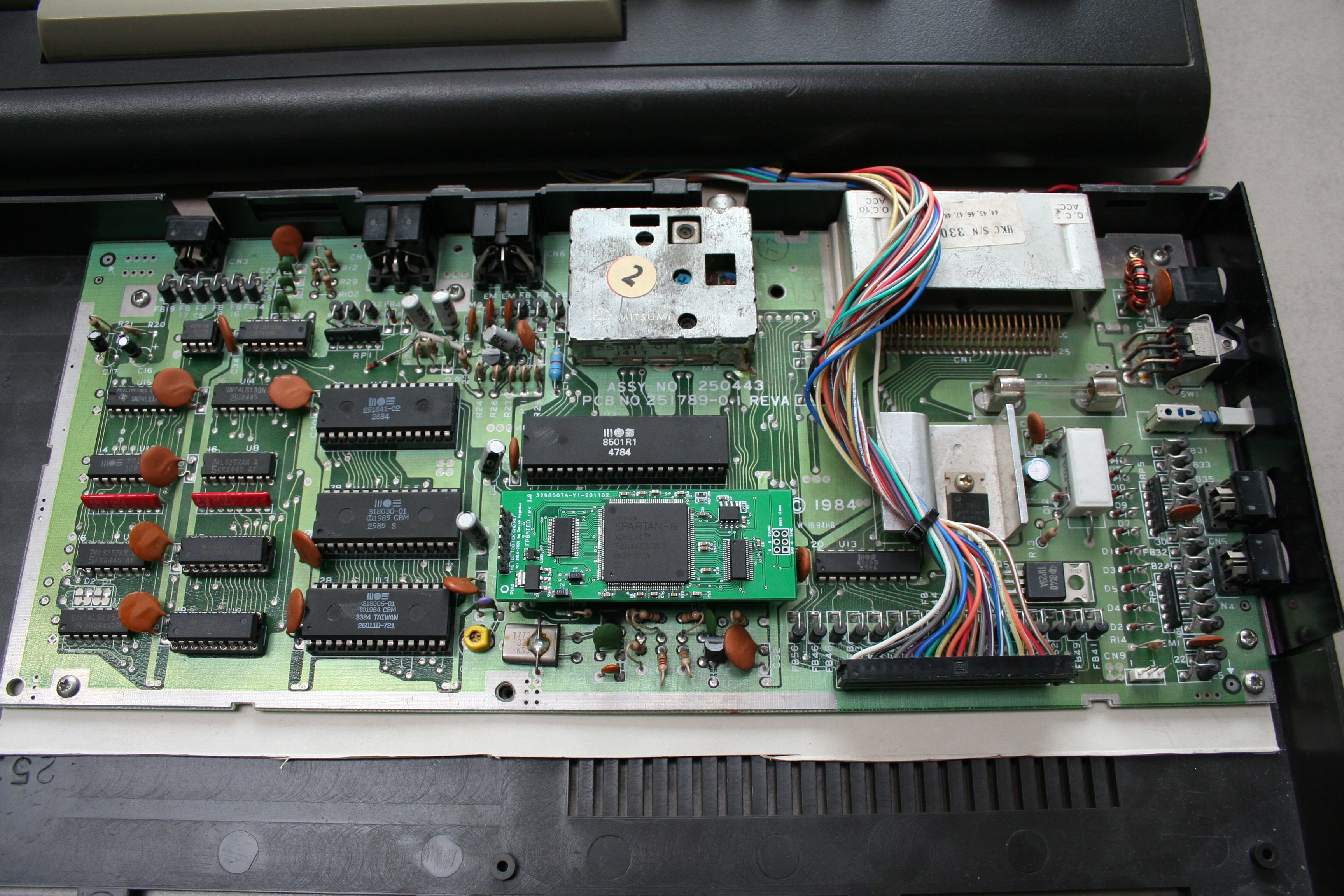
The size of PCB just fits into a Plus4's TED shielding and fits easily in a C16. Although I have tested it in both machines further testing is done using the C16 because it has more space and it is easier to load the firmware via the JTAG connector.
The board has two level shifters for those signals which need it. Outputs from TED's point of view don't need level shifting because they are LVTTL compatible, only bidirectional or input signals are translated. Interestingly the motherboard's clock signal stays under 3.3v (see PLus4 or C16 schematics which gives explanation) so it is directly connected to the FPGA. Two cascaded LDOs create 3.3v and 1.2v supply voltages from 5v. As the 2nd LDO is supplied from 3.3v the heat dissipation is minimal and the component stays cool during operation.
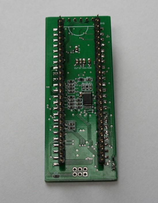
The backside of the PCB has an SMD IC header which together with the FPGA are the most expensive parts of the whole device. To keep cost as low as possible a Xilinx Spartan6 LX4 FPGA is used which still have empty space left inside for further improvements, but it can be replaced by an LX9 if needed (of course not by users). As the SMD IC header has still not yet arrived I had to create a temporary solution using straight through hole IC headers. As these are for through hole applications, the shorter pins which are normally soldered inside the PCB holes are now soldered to the smd pads. Benting them would break them so this was the easiest way to test the device without the final header. I was surprised how solid it is when soldered! The only drawback is that the device is now too high when inserted to the TED socket (which is not an issue in a C16, but might be problem in a Plus4). But hey this is just a prototype!
The components I have soldered with my hands (takes time but not that difficult when you have a microscope).
I was afraid that during power up the configuration of FPGA will not finish by the time the reset cycle finsihes (about 500ms), so in the design I have taken this into account. In order to speed up the configuration time during power on, the onboard SPI flash has a quad connection and the bitstream utilizes it with a 10Mhz configuration clock. Needless to say that it works perfectly!
I have programmed it via iMPACT and turned on the Plus4 with high hopes (yes, first I have tried it in a Plus4).
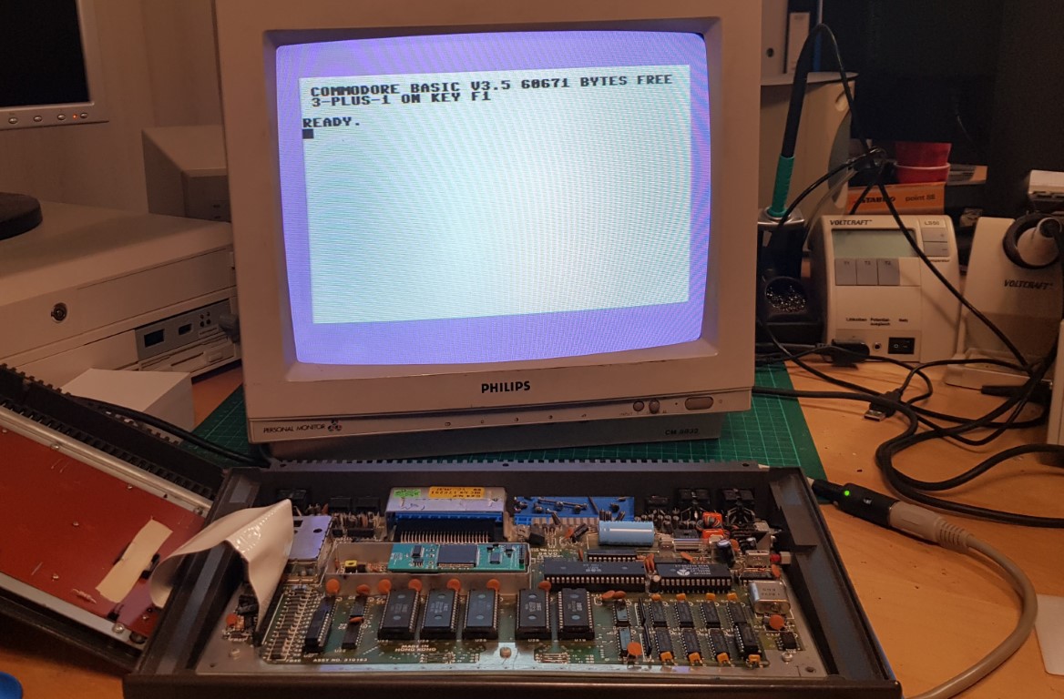
It works! Thanks to the careful design, individual part testing it works perfectly! The image is generated via the composite video out and RF modulator (I was surprised how much better the Plus4's RF modulator is compared to the C16. It gave much sharper and clearer picture). I have adjusted the color phases to be as close to the original as possible, I have even done measurements on real TED via oscilloscope and calculated phase angles from time differences between burst and color signals.
Since the first power on I have used it a lot and tested serveral games, demos. I have fixed DMA delay in TED core (see release latest source code) and now everything I tested so far works fine!
So what are next steps?
I am waiting for the smd IC pin headers and can build some more units (I have components for about 10 now), The PCB has an SRGB header also which I have not yet tested. What I regret is that this header does not have hsync/vsync just csync. So if I want to implement scandoubler I need to redesign this part.
- I am going to design a 4 layers PCB for the cheaper and smaller BGA Spartan6 using through hole pin header (v2).
- Create a mass production so that everyone can buy it
- VGA output
- HDMI output
- SID cart implementation inside the FPGA
Soon I will create a youtube video about how it operates and share its link here on hackaday.
Until that keep your eyes on the updates!
 István Hegedűs
Discussions
Become a Hackaday.io Member
Create an account to leave a comment. Already have an account? Log In.
Gran proyecto, estoy interesado pues mi plus4 quedó en el sueño de los justos, saludos.
Are you sure? yes | no
I can't wait to buy it to repair my beloved C=16
Are you sure? yes | no
Wow! This is great news!
I have a couple of old 264 boxes waiting for something like this to become available.
What about adding a memory upgrade to 64k into the next revision?
Are you sure? yes | no