Jon Thomasson
-
Video Demonstration
05/17/2018 at 17:19 • 0 commentsHere is a short video demonstration of the transceiver.
-
Houston, we have transmission!
05/07/2018 at 05:19 • 0 commentsI’ve been working more on writing firmware to test the transceiver modules. Although I couldn’t locate any ready made libraries to drive this particular IC, there were a few none the less that helped to guide me in the right direction. Those libraries were the RF69 library by Lowpower Lab, as well as the Radiohead library. These libraries interfaced with a similar model transceiver, the SX1231, which was also designed by Semtech.
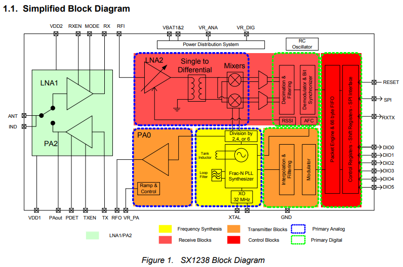
One of the features of the SX1238 that intrigued me was that it included not one, but two low noise amplifiers on its receive, as well as two power amplifiers on its transmit. These added amplifiers should not only make it easier to detect weak signals, but should also give the transceiver a theoretical longer range as compared to the SX1231. Here is a view of the block diagram for the SX1238 showing how the internals are laid out.
![]()
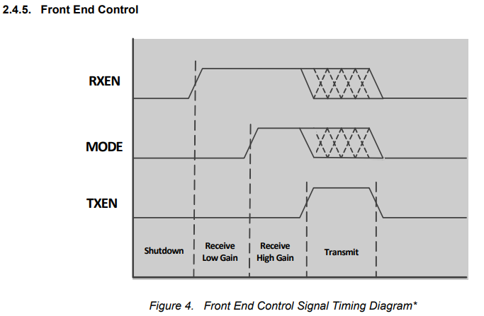
These added amplifiers, PA2 and LNA1, are turned on/off through three front end control pins, TXEN, RXEN, and MODE. The operation of these pins through the different transmit/receive modes can be seen here:
![]()
Interfacing with these pins was of course just a matter of connecting the appropriate pins on the transceiver module to the arduino and then toggling them during the transmit and receive sequence.
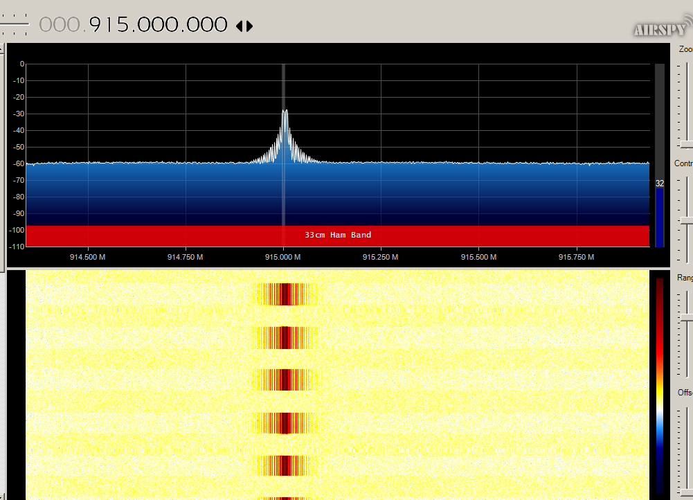
To test the transmitter I used a cheap RTL-SDR dongle and the free SDR Sharp software. I just wrote a simple sketch which transmits a packet once a second and looked for the signal to show up somewhere on the FFT plot. It was a thrill to see the signal pop up on the screen for the first time! It was alive!
![]()
After this euphoria, I thought setting up the receiver would be the easy part. Boy was I wrong! The firmware for the receiver was setup to simply listen for incoming packets from the transmitter, and then print those packets out to the serial monitor. The excitement was nearly unbearable the first time I uploaded the firmware to the receiver. Expecting to see a rush of packets fill the serial monitor screen, instead there was nothing. Just a blank screen. The roller coaster thrill ride came crashing down and hit with reality.
There was an onslaught of doubt in my mind after this initial test. Maybe there was something wrong with the pcb, or perhaps there was a faulty solder connection somewhere. It was obvious that something was being transmitted since the signals were being picked up by the SDR Sharp software. However, maybe the actual transmission was just garbage.
After taking a break for a bit and getting some air, I decided to dig through the datasheet again and analyze my code a bit more. This digging led me to discover a peculiar register named RegFifoThresh that had as one of its variable names TxStartCondition. TxStartCondition, as its name implies, determines the state at which the transmitter would begin transmitting packets from the FIFO. By default this register was set to only transmit after a specified FIFO threshold had been passed. Since I wanted the transmitter to transmit whenever there was a new packet in the FIFO, I changed this default value to allow the transmitter to transmit whenever the FIFO was not empty. After making this modification and uploading the firmware once again, I started to see a few packets being received and printed out on the monitor. However, the packets weren’t consistent, and the data wasn’t recognizable. But it was progress!
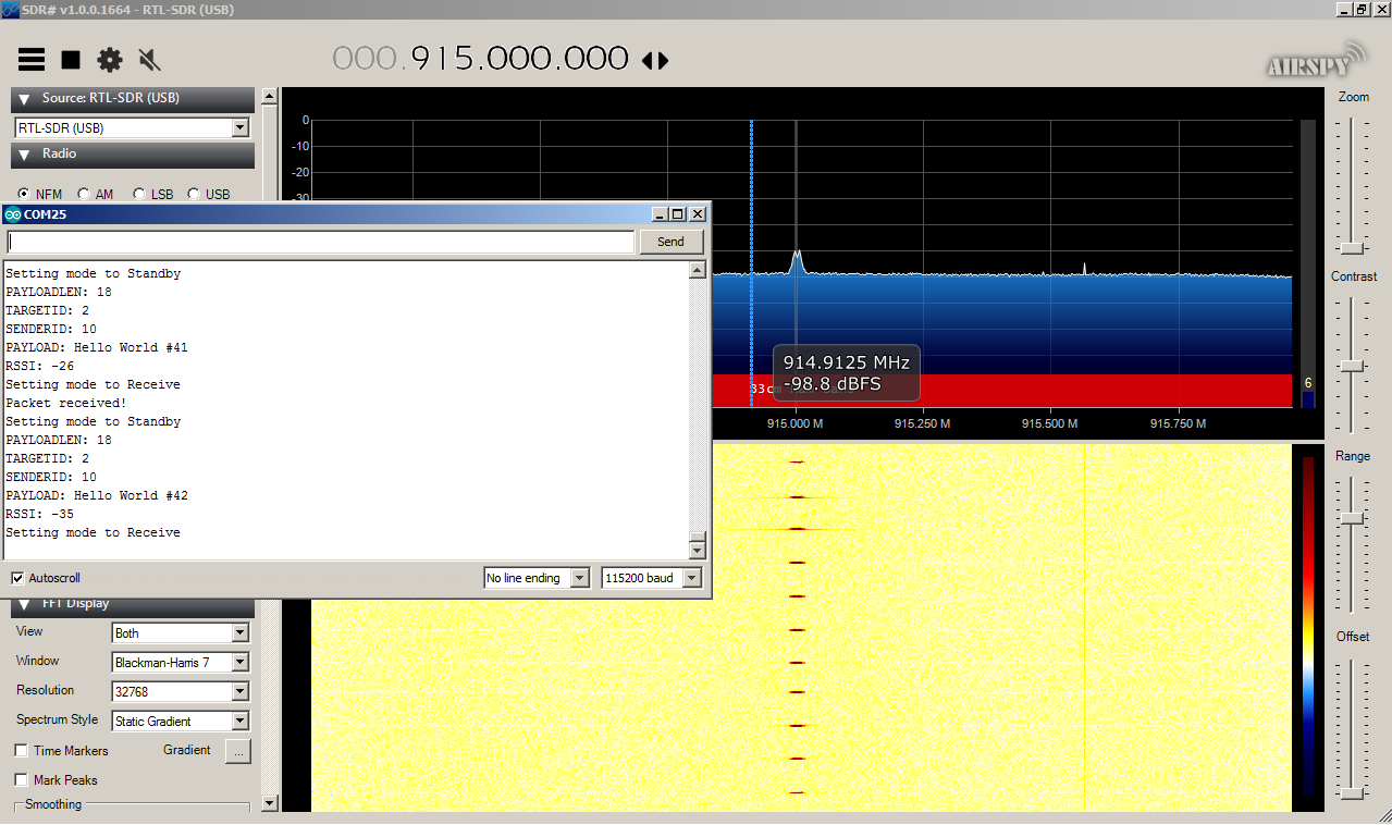
I ended up experimenting for some time with all the various filters and frequency shaping registers. It was fascinating just to make some changes to a few registers and see how it affected the look of the signal in SDR Sharp. I finally cleared the registers pertaining to the frequency deviation of the signal, and reset it to its default parameter. And low and behold, I started receiving packets! I had modified these register values when porting some of the code from the other libraries into my own. It’ll require a bit more experimentation to see what the optimal frequency deviation will for various bit rates, but for now at least I know the design works!
![]()
As with all projects, you tend to learn more from the things that don’t work the first time. And this project was no exception. I’d like to think that I have a new appreciation for RF, and just how delicate a balance it can be to get things to behave just right. My oldest daughter and I are in the process of studying for our HAM radio licenses (I currently hold a Novice class) and it was educational for us to see the correlation between these things (frequency deviation, bandwidth, side band) we’re reading about, and viewing them live via the SDR software.
-
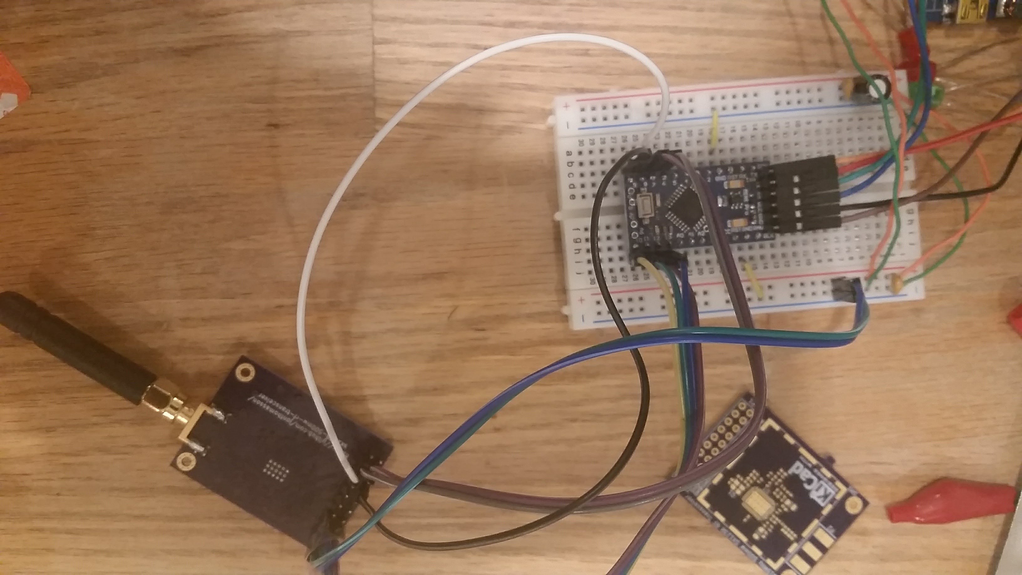
SPI testing and register read/write
04/26/2018 at 13:12 • 0 commentsThe boards passed the initial magic smoke test. I brought the boards up with a current controlled power supply and to my surprise no magic smoke escaped! After that I wired up the SPI bus to an 3.3v Arduino pro mini to see if I could communicate with the transceiver.
![]()
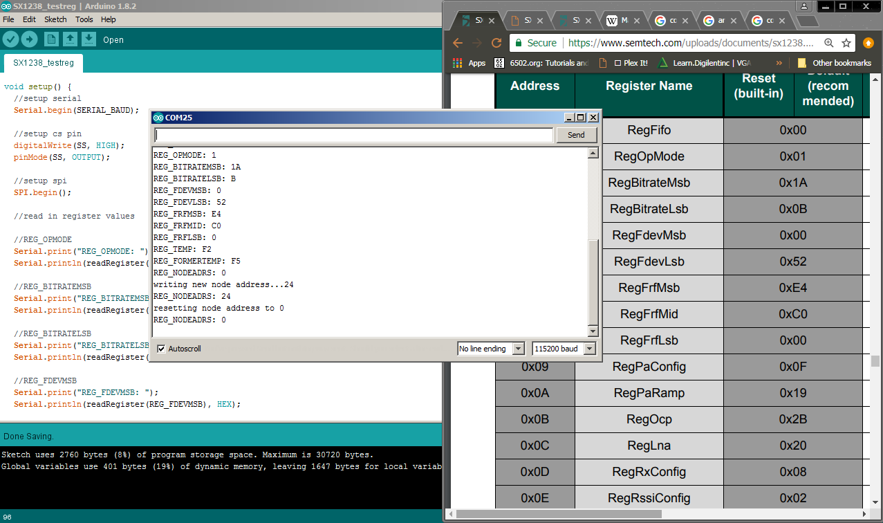
I wrote a simple sketch that reads/writes to various registers. The idea here is that if the SPI bus isn't working, it's pointless to do any further testing until that can get sorted out. The sketch simply reads the register data to a serial console so I can check it with the default parameters of the datasheet. Here's the results from the SPI testing:
![]()
It looks like the register values match! Cool, so onto transmitter testing next…
-
Built 2 boards
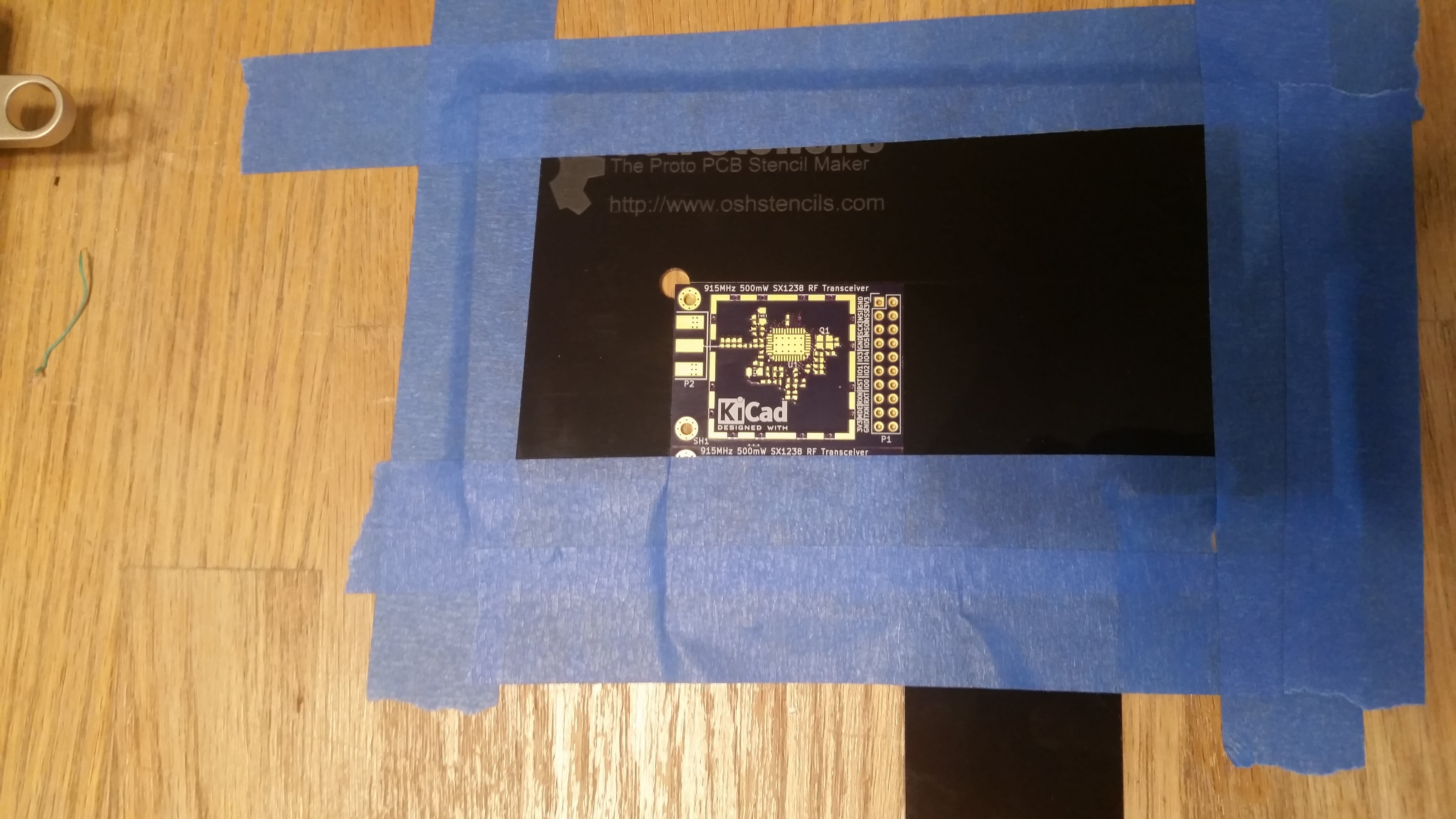
04/20/2018 at 22:38 • 0 commentsI got packages from oshpark, digikey, and oshstencil back recently so I decided to make some time to put a couple boards together. I have to admit that I was nervous just thinking about hand soldering these boards, given the close proximity of several small 0402 components and the large ground pad under the transceiver chip. For this reason I thought it would be a good time to try out a solder paste stencil.
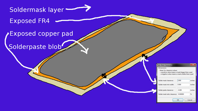
Since I hadn't done a stencil before, there was a bit of a learning curve. I found some resources that helped me get started. The first was this page from rheingold heavy which introduced some of the parameters needed, such as the solder paste clearance, to get the gerber files ready to send to oshstencil. The second resource was from this forum post on the kicad.info forums. Specifically this picture helped me visualize how the pad mask parameters in Kicad worked :
![]()
The first step for me was to determine which pads on the PCB required a stencil. At first I was thinking about just including all the SMD components. But after giving it some more thought I opted to leave out the SMA connector and shield, since I wanted to be able to test the circuit out first before sealing it in its metal house. And the SMA connector would require some hand soldering to get a good connection.
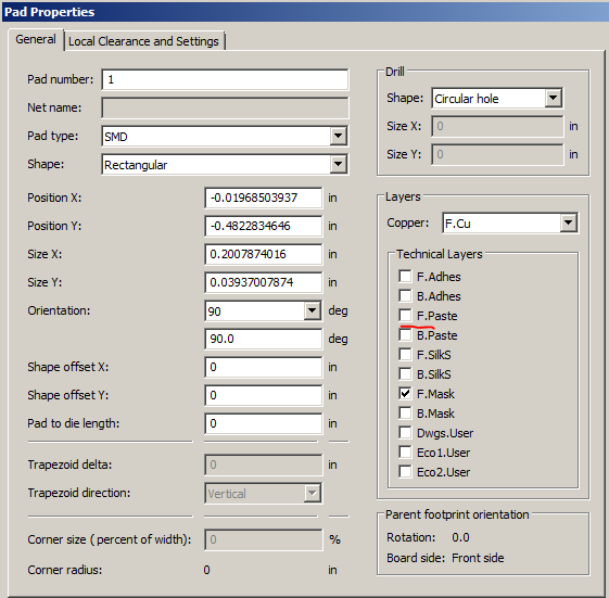
Now that I knew which SMD pads I wanted to exclude from the stencil, I took those pads out of the stencil by unchecking the F. Paste layer (the front solder paste layer) from the Technical Layers area of the Footprint Editor. This disassociates the pad from the front solder paste layer. It looks like F. Paste is checked by default whenever you create a new SMD pad.
![]()
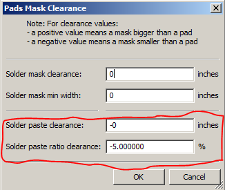
The next thing I learned was that there should be a little bit of clearance between the solder paste and the edge of the pad. This clearance is aptly named "Solder Paste Clearance" and is illustrated on the picture above. This property can be adjusted on a per pad level on the pad properties page, or on a global level. To set the clearance for the entire PCB you navigate to Dimensions -> Pads Mask Clearance from the Pcbnew screen.
![]()
On the Pads Mask Clearance screen, there are 2 options for adjusting the solder paste clearance. You can either choose to set the clearance a fixed amount from the edge of the pad, or you can set the clearance to be a ratio based on the size of the pad. I chose to give the clearance a ratio of -5%. After adjusting these properties, the only thing left to do was to generate the gerber files which will be sent to oshstencils. When you go to generate the gerbers, you only need to select the solder paste layer as well as the edge cuts layer, since those are the layers that oshstencils care about.
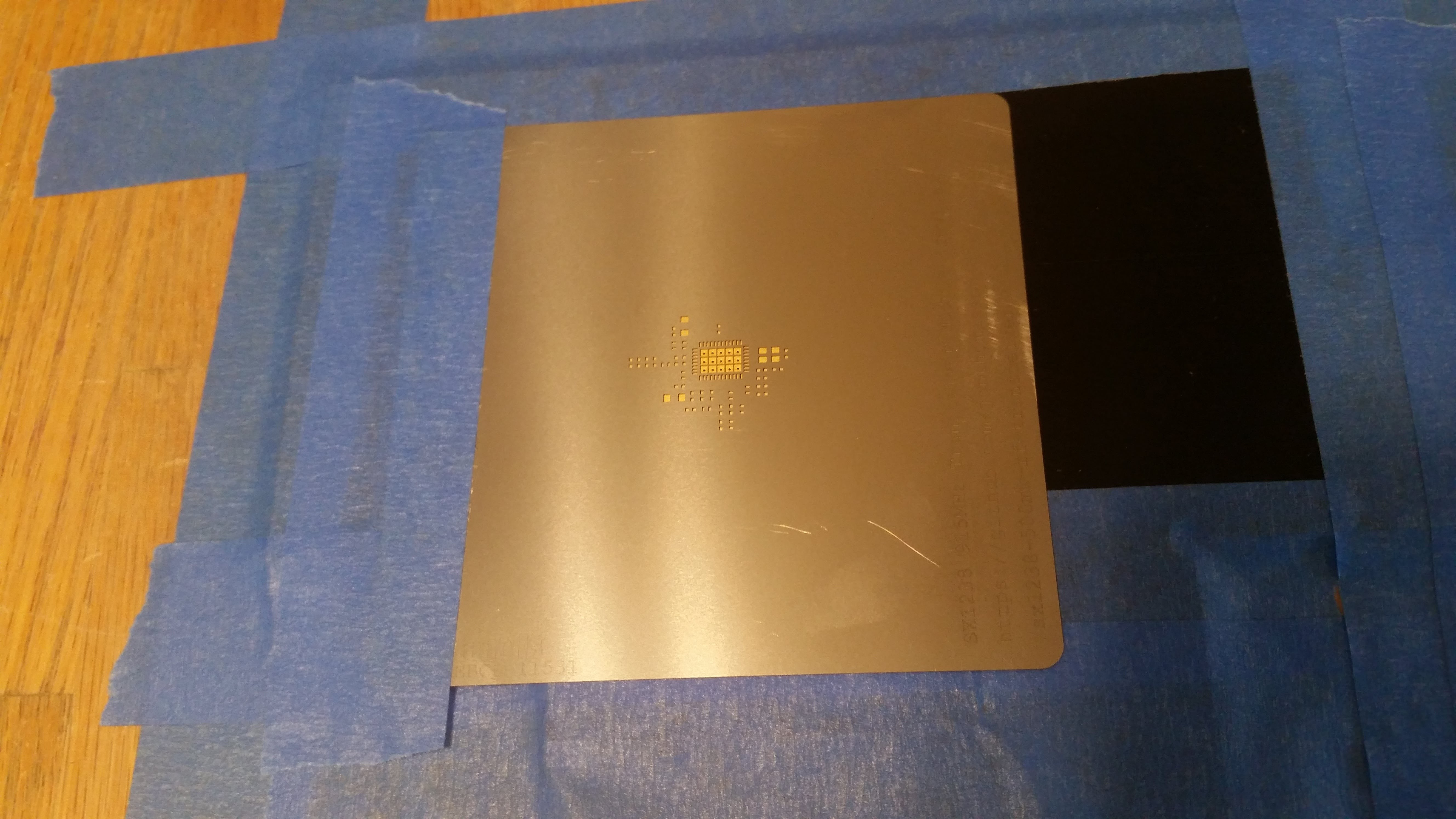
I was surprised at how quickly I received the stencil back. It seemed like it only took 2-3 days from the time of order to having the stencil in my hand! Besides the stencil, I also ordered a little jig to hold the stencil in position while applying the paste. I found out you can also just use unpopulated PCB’s to fashion your own jig. Here’s a pic of what I came up with:
![]()
Once the jig and PCB are in place, you lay the stencil over the PCB until all the pads match up and are visible through the appropriate cutouts of the stencil. Then you tape the stencil down on one side.![]()
From here, my pictures were a little too blurry to share, but I basically followed the same procedure for applying the paste presented in this Sparkfun video. The important thing I learned from all of this was to make sure to clean up the solder paste from the stencil and anything else you want to keep right away. Otherwise it really gets tough to clean up, and it manages to get everywhere!
To reflow the solder paste after I had placed the components I simply used a hot air rework gun. I did have some solder bridges around one of the transceiver chips, but nothing a little drag soldering couldn’t fix. Here’s the finished boards (with a quarter for size reference):
![enter image description here]()
500mW (27dB) ISM Band Transceiver
This is an ISM band transceiver utilizing the Semtech SX1238. Similar to the popular RFM69 except with an added power amplifier on transmit.