Ted Yapo
-
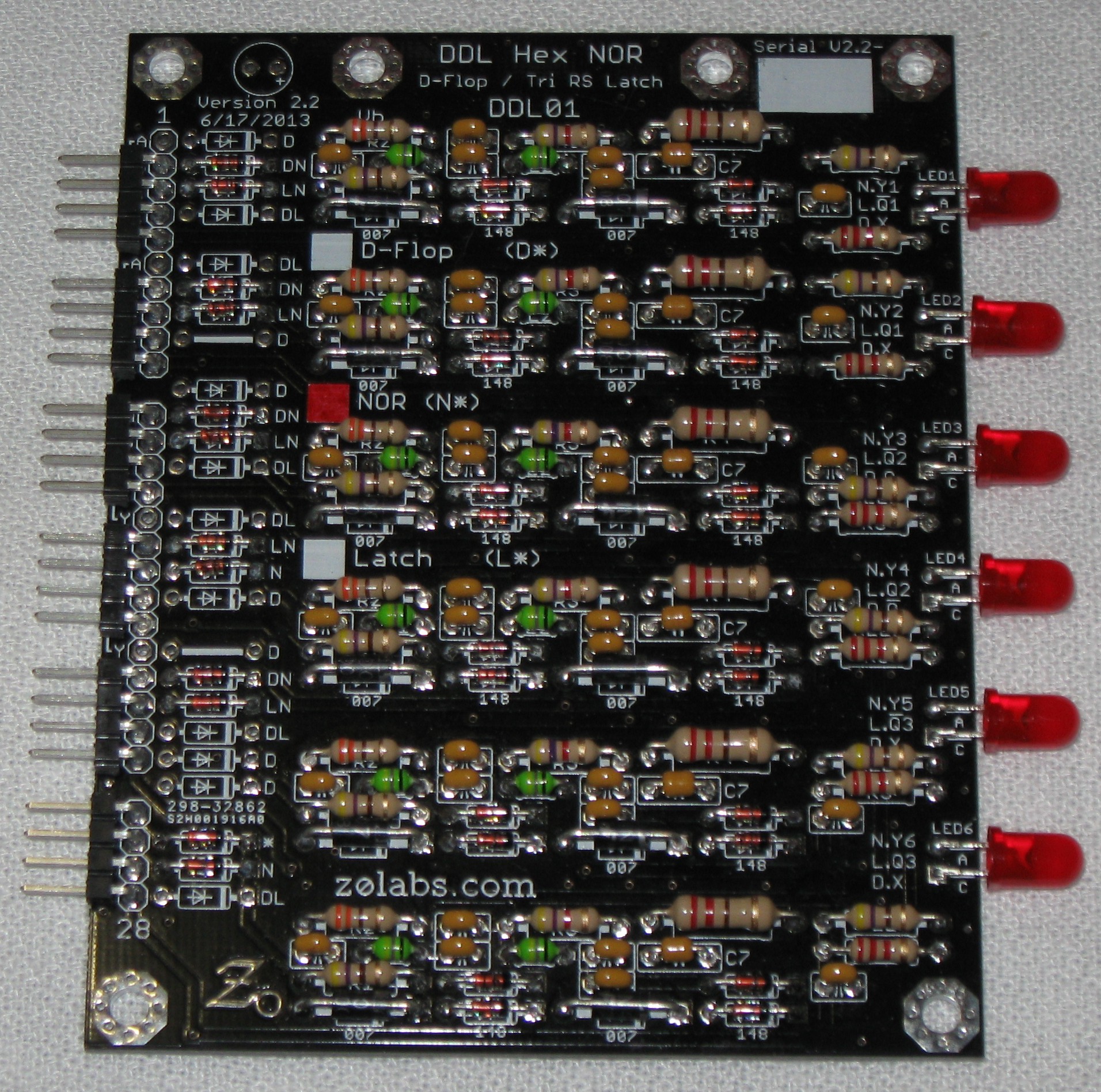
DDL01 Hex NOR Gate
05/14/2016 at 00:55 • 0 commentsI added an introductory video to the project details. No particularly new information, but you can see the thing run through 24 hours in a matter of seconds. Nice for fans of das blinkenlights.
Design of DDL Gates
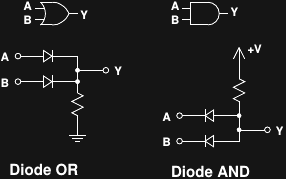
Just for reference, here are the traditional diode gate circuits:
![]()
These work fine for a small number of stages, but these are the only gates they can form.
Single-Stage DDL
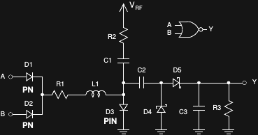
The first real attempt I made at a usable diode logic family, DDL 1.x, used single-stage NOR gates, like this schematic:
![]()
More details about this circuit can be found in the DDL Backgrounder pdf, although I know it's not the clearest technical writing. It's a diode-OR gate, a shunt PIN-diode switch and an output voltage doubler. I think if you built single-stage gates like this with an actual PIN diode at D3 and Schottky's at D4 and D5 as shown in this diagram, you might have a chance at a scalable system. Once I got it into my head that I was going to use more common diodes (purely for gratuitous shock value), I had to abandon single-stage designs. This set me back at least a year. The problem is that single-stage gates with 1N4007/1N4148 just don't have the current drive / fan-out to create large systems. I was able to get simple D flip-flops to work, and even a Johnson counter, but I couldn't easily cascade counters - there simply wasn't enough gain in the devices.
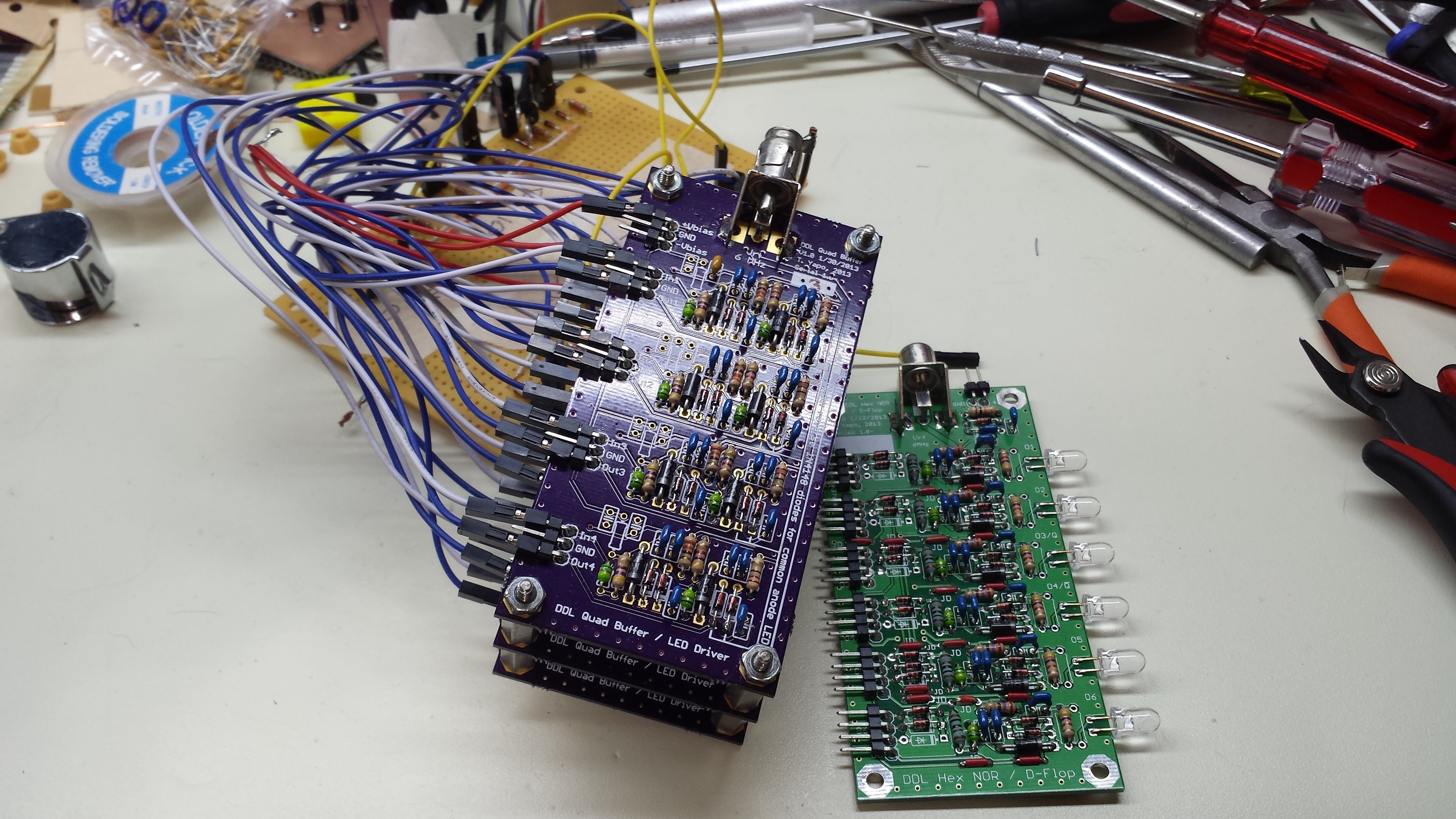
Even early on, I knew I needed two-stage gate to drive the display segments to reasonable brightness. Here's a pic of the first two-stage PCBs - the purple boards are quad two-stage drivers, while the green one is a single-stage hex NOR. This "stack" is wired as a mod-4 Johnson counter, using the 12 gates as two D-flops. It was this prototype that convinced me I needed two stages everywhere - it's been wired like this in the junk box ever since. I really did like the form factor of the single-stage boards. At 2x4", they were much more compact, quicker to assemble, and cheaper (!) than the latter generation.
![]()
Two-Stage DDL
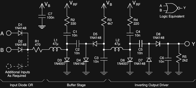
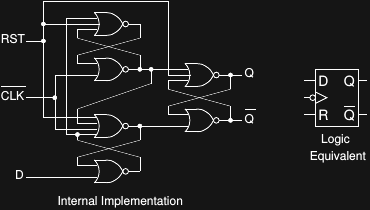
The topology of two-stage DDL gates are explained fairly well in the datasheet, but I can't resist hitting the highlights here. Each of the six gates on the DDL01 board look like this:
![]()
Omitted from this diagram are the front-panel LEDs and dropping resistors (640nm red and 470 Ohm from Y to ground).
The key to good current drive from the output stage is getting D6 to turn off completely. The problem is that 1N4007's have a fairly large capacitance (the datasheet says 15pF at 4V reverse bias; I measure a better figure of 15pF at 0V), plus, they're lousy PIN diodes. By applying negative bias to D6, the off-state impedance is greatly improved, allowing much more power through the output voltage doubler (C5, D7, D8, and C6). This kind of negative bias is universal practice in "normal" RF PIN diode switches. In this circuit, the voltage doubler (D4 and D5) on the first stage is reversed, so it outputs a negative voltage, overcoming the positive bias through R3.
You might think you could just use a negative bias at VB to keep D6 off. The problem is that when D4 and D5 are wired as a positive doubler, they clamp any negative bias through R3 to two diode drops, or about -1.4V, which simply isn't enough to turn D6 completely off. In the negative doubler configuration above, D6 holds its own positive bias to 0.7V, so D4 and D5 don't interfere.
It took me way too long to figure that one out.
D Flip-Flop
The driving force behind the decision to put six gates on a package was being able to make an edge-triggered flip flop, shown here:
![]()
By populating the right input diodes and jumpers on the DDL01, all these connections can be done on the board, and it can just be treated as a flip-flop. It makes great counters and shift registers, and seems like just the thing for program counters or register files. Think of it as a "DDL74" (you can wire in a "Set" input as well with a few more diodes, but it's not on the current board rev., so it has to be wired externally).
I have to acknowledge Ken Bigelow's play-hookey.com site here. I had seen edge-triggered D flip-flops made from NANDs before, but after about a half hour trying to design my own NOR version, I found his (NOR D-Flop @ play-hookey.com) diagram, and based my design on that one. Thanks, Ken!
Of course, I could have just DeMorganized and reduced the NAND version, but the internet is much faster than I am.Design Files
This is what the DDL01 looks like (in basic black):
![]()
If you want one (or 46), you can either:
If you'd rather just simulate the board, here's an LTspice simulation file for a single gate from the DDL01. As with all things SPICE, take the results with a grain of salt (pun intended). I only found the simulations really useful when I couldn't be at the bench for some reason, but they're fun to play with.
The files are licensed CC-BY-SA.
-
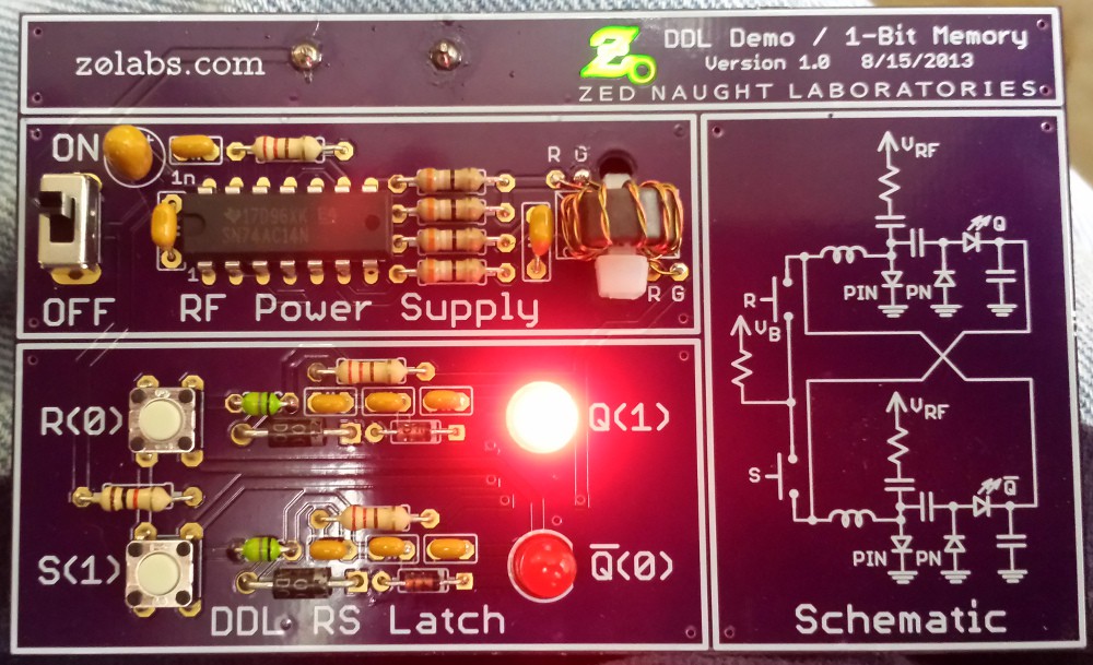
DDL Demo Board and Simple Examples
05/13/2016 at 16:26 • 7 commentsSince the Diode Clock is fairly large and complicated, I wanted a smaller example to demonstrate how simple diode logic gates really are. The result was the DDL demo board (shared here on OSH Park). The design files (Eagle schematic and board files as well as LTspice simulation file) are shared here on hackaday.io. I've included decent models for the 74AC14 used in the power supply, and of course, for the 1N4007 diode, so the whole circuit can be simulated in LTspice. If you're willing to wait for it.
The board looks like this:
![]()
This perfect purple board was (obviously) fabbed at OSH Park; Laen wrote somewhere about people drawing schematics on the silkscreen layers of their boards - when I read that, I knew it was exactly what I wanted. The idea is to have a pocket-sized demonstration of the simplest diode-based logic circuit you can't build with "traditional" diode logic (AND and OR gates). It's an RS flip-flop that stores its state in six diodes: two 1N4148's, two 1N4007's, and two red LEDs, which double as indicators. With four AA batteries on the back, it can store a single bit of your choice for as long as the batteries last (~48H - it's a power hog). A more complex version of this circuit was what convinced me in 2008 that universal diode-only logic was possible. I think this is probably as simple as you can make it.
Here's a silent film of it in "action":
Now, what's the coolest information you can store in a single bit?
The latch circuit
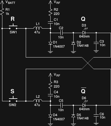
Here's the latch circuit schematic:
![]()
The top portion associated with D1 and the bottom associated with D4 form two inverters. When DC current flows through D1, it shunts the RF current through R2 to ground, producing no output through D3. meanwhile, the lack of DC current through D4 results in a high impedance to ground for RF, which energizes the voltage doubler consisting of D5/D6, closing the feedback loop, and maintaining the current state. If you then press SW2, D4 starts to conduct, and the roles reverse, storing the opposite state. More info can be found in the datasheet.
The LEDs deserve some special attention. I specifically used 640nm LEDs (Kingbright WP7113SRD/E @ Digi-Key) because of their high brightness and low Vf (1.85V @ 20mA). Both really help in not overly loading DDL outputs. If you can afford them, the /F or /G grades of that part are even brighter - every little bit helps. I've also tried fairly random LEDs, and found the results to be hit or miss. This morning, I breadboarded a version of this circuit with some junk-bin green LEDs and a simpler power supply but had to turn off the shop lights to see that it was working (see below).
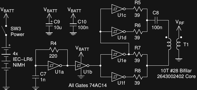
DDL Power Supplies
The RF power requirements of DDL logic gates are the most difficult aspect of these bizarre circuits. The DDL02 power supply board took seven fairly major iterations to get "electrically right", and it probably could use an eighth for thermal issues. I'll be documenting those tribulations shortly. Even simple DDL circuits like the demo board can be fairly picky about the RF supply. Here's the supply on the demo board:
![]()
In a somewhat perverse twist, I'm using a 74AC14 hex Schmitt-trigger inverter as a power supply for the diode logic circuit. An RC relaxation oscillator made with one gate (U1a) drives a buffer stage (U1b) before a push-pull stage (U1c - U1f) AC coupled to a broadband transformer to generate the required RF supply for the DDL circuit. The 74AC series is plenty fast, the outputs can source or sink 24mA with symmetrical output impedance, and it has edge rates near a nanosecond. They're some of my favorite analog parts. Don't substitute an 74HC14 or TTL part here; they won't drive enough current. This supply runs at about 3.6 MHz, depending on component tolerances and temperature/
I wound the transformer on a Fair-Rite 2643002402 core, because I have a large bag of them. It's intended for EMI shielding, but it's just a core of 43-type material that's really cheap, and makes great broadband transformers. An alternative is the Laird 35T0501-10H @ Digi-Key, which will work just as well. Any core designed for use at HF, like the Amateur-radio favorite FT37-43, would also work.
Alternative Supply
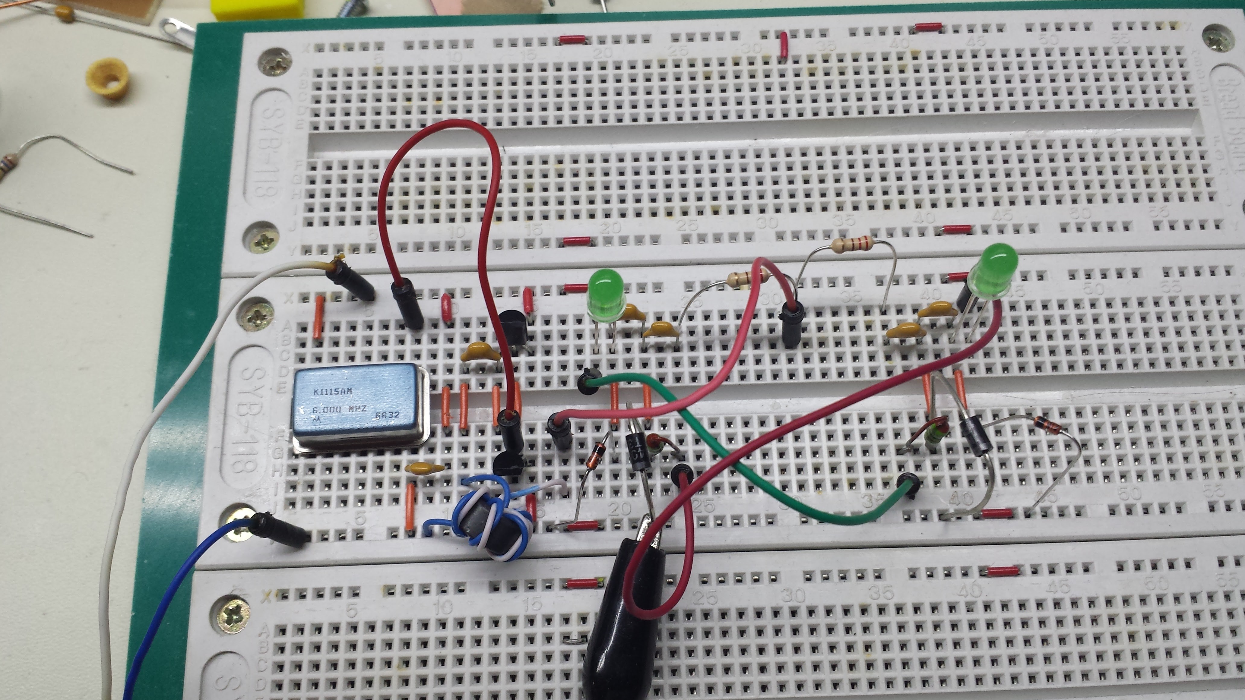
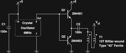
I realize that not everyone will have a 74AC14 lying around, so I breadboaded another simple supply and latch this morning using a 6MHz oscillator can from the junk bin:
![]()
The latch is identical to that described above, except for the use of "random" standard-brightness green LEDs. The power supply looks like this:
![]()
Q1 and Q2 are wired as emitter followers to boost the current output from the oscillator (and we accept the 1.4V of lost voltage swing). Any complementary pair should work here (2N3904/2N3906 or 2N2222/2N2907 come to mind). C2 blocks the 2.5V DC component of the output to avoid loading Q1 excessively. Finally, T1 is wired as an auto-transformer to boost the RF voltage by a factor of two. This circuit would probably work with oscillators from 3 to maybe 10 MHz. I briefly thought of using the internal RC oscillator / clock output option of a 4MHz PIC microcontroller (with no code running) to drive the transistors, but figured the oscillator can was (slightly) easier. For the transformer, I didn't feel like twisting up a pair from magnet wire, so I just used a section of twisted pair from a CAT5 cable. I could only fit about 5 turns on there, but it still works well enough for a quick demonstration.
Between the thrown-together power supply, the lousy green LEDs, and maybe parasitic qualities of the breadboard, the performance isn't great. I had to turn off the shop lights to see it, but it does still work as a latch:
-
Short-Term Plans and Problems
05/13/2016 at 03:39 • 0 commentsJust a quick update to get me familiar with project logs on hackaday.io, and into the habit of sharing.
Documentation
I added a bunch of PDF documentation to the project today. I had it lying around, and figured between the various documents, you could get a good idea of how this project works:
- DDL Backgrounder : a dryly-worded introduction to early single-stage DDL gates. If you've never seen a provisional patent application before, they might look a little like this years after they've expired. Single-stage DDL gates suffer from poor fan-out, and are difficult to make work in large designs. I don't hold any patents in any country I that know about, for anyone wondering.
- DDL01 Datasheet : When I first thought about building a computer with diodes, I imagined what parameters I'd want to see on a datasheet for the gates. Then I figured I might as well write one. This is DDL 2.0, which works well enough to build large-scale systems. 46 of these boards are used in the Diode Clock.
- Minutes / Seconds Counter Wiring : A schematic and wiring diagram for the seconds and minutes counter stacks. Each stack consists of (11) DDL01 boards wired as two decoded Johnson counters, a mod-10 counter for the ones digit and a mod-6 counter for the tens. These probably could have been optimized, but I wanted the logic-level design to be "easy" having spent so much time getting the gates to work. The counters are wired "by hand" with 30ga wire-wrap wire, then soldered for good measure. It was no picnic - see below.
- Hours Counter Wiring : Schematic and wiring diagram for the hours counter stack. Again two decoded Johnson counters (mod-10 and mod-3), but with 24H detection and reset circuitry, which uses a belt-and-suspenders reset latch to ensure both digits are reset to "00" before releasing the reset signal. I was afraid of violating minimum reset pulse times here.
- DDL Demo Board Datasheet : I've tried to come up with the simplest DDL logic circuit that you can't build with "traditional" diode AND or OR gates. This might be it - an RS latch using two 1N4148s, two 1N4007s, and two LEDs. The LEDs are used as part of the RF voltage doubler. The datasheet explains it all.
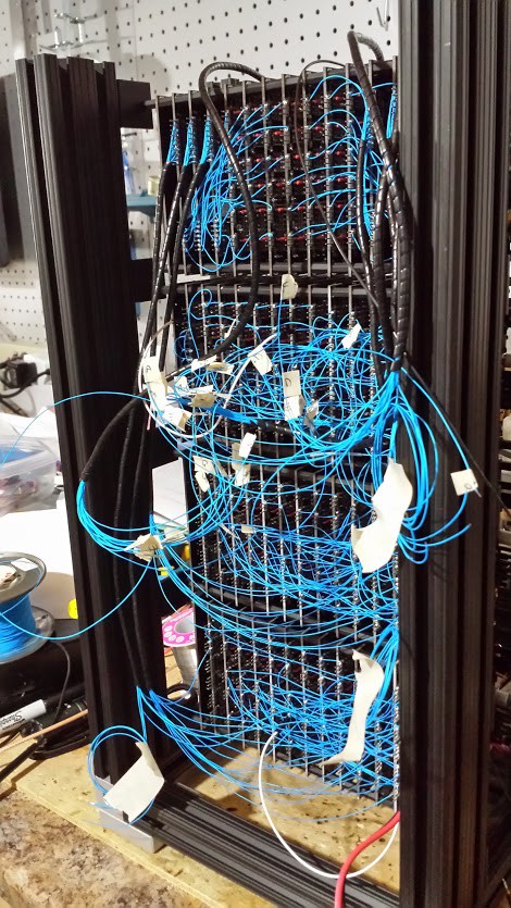
Wiring the Clock
It wasn't as fun as it looks...well, OK, it was :)
![]()
Two Problems
Open Documentation Source
I have two problems at the moment. First, in the spirit of open-source, I am willing to release the source code for the above linked PDF documentation under an open-source license if anyone is interested. It's nightmarish latex and xfig and gnuplot, but hey, some people actually like that kind of drudgery. Let's leave it at that - if anyone wants to create a derived work from that documentation, let me know, and I'll release it. I am going to release the board design files, though, even if nobody asks ;) This brings me to the second problem.
Inductor Sourcing
After I made my first prototype DDL gate, I looked around for suitable inductors, which were shaping up to be the most expensive part of the design. I found a great deal on super-miniature 47uH formed-lead chokes (Taiyo Yuden LAL02VD470K) on ebay, and bought all the seller had, because they were very cheap, and I had dreams of building a full computer with DDL. They were so cheap because they were discontinued: I believe I have world's remaining supply - five boxes of 2,000, minus the 500 or so I've used.
So, here's the problem. Nobody seems to make through-hole inductors in this size any more, so if you use the PCB designs as-is, you can't buy inductors that fit easily. If anyone wants to build DDL boards, I think there are three options:
- Re-design the boards to accept larger through-hole (or SMD) inductors which are readily available. The boards are tight, but it might be possible.
- Use the existing PCB design with larger inductors mounted vertically on the boards. Clearance to next boards in a "stack" might be an issue.
- Ask me for some of my inductor stash, and we'll work something out
In any case, I'll be working on releasing the design files in the next week or so.
Next Steps
I'll be releasing the design files for the various boards, including:
- Eagle PCB Design Files: I already have gerbers up on OSH Park for most of them (not currently shared), but I'll be putting Eagle files up there and here on hackaday.io, too. I used OSH Park for the many generations of prototypes, but for the Diode Clock, the boards absolutely. had. to. be. black.
- LTC Spice simulation files: Yes, you can simulate DDL gates with Spice. The trick is having a good model for the 1N4007.
The plan is to document and release things in roughly this order:
- DDL Demo Board
- DDL01 Hex NOR
- DDL03 Hexadecimal to 7-Segment ROM
- Simple DDL circuits to experiment with
- DDL02 "Chainsaw" Power Supply
- DDL04 "Whisper" Spread Spectrum Exciter
- TCXO Timebase and diode-only oscillator timebase experiments
Zed Naught LaboratoriesIf you look closely at some of the design files, you'll see my company, Zed Naught Laboratories, LLC, and the alternate domain z0labs.com. Don't worry, I'm not trying to sell you anything. It's not that kind of company.
The Diode Clock
A digital clock built with Diode-Diode Logic (DDL), a quirky new logic family using only common diodes and passive components.