Ted Yapo
-
Testing Methodology for Substitute Components
07/30/2016 at 21:34 • 0 commentsI haven't posted a log on this project for a while. Since last time, this project was selected as a semi-finalist in the Hackaday Prize 2016. I was really blown away to see this. Seriously, this project consumed my thoughts and my life for a long time, and it's awesome to have it recognized in this way. Thanks to all the decision makers for their consideration!
Substituting Components
There are a few component substitutions I need to test. First, the original inductors on the DDL01 boards are no longer in production - in fact, no inductors in that package seem not to be made in 2016! I found some possible replacements, but before I re-spin the tightly-packed board, I figured I should test them out with the existing PCB. I had to order some more boards for this. and they're arriving tomorrow, so it's time to prepare for the tests.
The second substitutions are for the 1N4007 diodes. RF PIN diode switching is an "off-label" usage for the 1N4007, marketed as a rectifier diode, so the performance isn't guaranteed by the manufacturers' specifications. The first ones I tested worked, and I stuck with that manufacturer (Fairchild). I now have samples of 1N4007's from all the manufacturers I could find, and I'm going to see if they perform just as well (or better) than the original parts.
Finally, I'm going to test substitutions for the ferrite cores used in the DDL02 power supply. I remember being intimidated by the prospect of winding magnetics like this when I first started with RF circuits, and would like to run some quantitative tests to show that the inductors and cores used here aren't particularly critical (apart from getting the wires connected correctly). Hopefully, I can allay any apprehension prospective builders might have about these components and the power supplies.
I'll have to wait for the DDL01 boards to arrive to test the new components, but I can outline the testing methodology and run some baselines with the original components in the interim.
DDL01 Testing
I came up with a few ways to test the performance of the DDL01 gates. Here's a brief overview:
Eye Diagrams
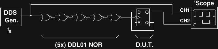
The first test is designed to examine the performance of a single DDL gate. One of the difficulties in this test is creating a "DDL" input waveform to drive the device-under-test. Around the lab I have either 50-ohm signal generators or 5V CMOS outputs, neither of which is a good approximation of a DDL output. My solution is to use a chain of DDL01 inverters to condition the signal before input to the D.U.T. Of course, now you're testing the whole chain, but major differences in performance of the D.U.T. due to component substitutions should be detectable.
Here's the test circuit. I use a DDS generator to make an accurately adjustable clock driving the CLKin pin on a PIC 16F723A. I had a handful of "breakout boards" made for this part since I've used it in a few projects and have a partial tube of them left over. The PIC is programmed with a simple 9-bit linear feedback shift register producing a 512-bit pseudo-random bit stream. The inner loop of the assembly code is 12 cycles long; combined with the CLK/4 oscillator divider, this results in a 1/48 clock division. Not great for high-speed work, but perfectly adequate here. One of the PORTB pins outputs the pseudo-noise sequence while another outputs a synchronized clock for triggering the scope.
![]()
In case anyone's interested, here's the simple PIC assembly. It uses the carry bit in the status register as part of the 9-bit shift register since the RRF instruction rotates through the carry - an easy way to double the length of the sequence without introducing more instructions.
;;;
;;; PIC16F723A LFSR pseudo-random bitstream generator
;;;  using 9-bit LFSR (regsiter + carry bit)
;;;   with polynomial x^9 + x^5 + 1
;;;
    LIST        P=16F723A
#include    <p16f723a.inc>
    errorlevel -305			;suppress warnings about default file dest
    errorlevel -302			;suppress warnings about operand not in bank 0
    errorlevel -227     ;suppress warnings about RETLW 0 instead of RETURN
    __CONFIG    _CONFIG1, _FOSC_EC & _WDTE_OFF & _PWRTE_OFF & _MCLRE_ON &_CP_OFF & _BOREN_OFF & _BORV_19 & _PLLEN_OFF
    __CONFIG    _CONFIG2, _VCAPEN_RA5
    #define   FEEDBACK_MASK  0x10
    cblock 020
      shift_register
    endc
    ORG     0
RESET:
    BANKSEL TRISB
    movlw   b'00000000'         ; set PORTB to all outputs
    movwf   TRISB
    BANKSEL ANSELB              ; make PORTB digital
    clrf    ANSELB
    BANKSEL PORTB
    movlw   0xff                ; LFSR initial state
    movwf   shift_register
MAIN_LOOP:
    movf    shift_register, W
    andlw   0x1f
    nop
    movwf   PORTB
    movlw   FEEDBACK_MASK
    btfsc   STATUS, C
    xorwf   shift_register
    rrf     shift_register
    movlw   0x20
    iorwf   PORTB
    goto    MAIN_LOOP
    END
The schematic shows a DDL standard load (470 ohms plus a 1N4148 and 1N4007) attached at the output, but I omitted that load for the following tests. Here's what the eye diagram looks like at various frequencies. I changed the timescale with frequency to keep the eye size relatively constant:
![]() 1 kHz
1 kHz
![]() 2 kHz
2 kHz
![]() 3 kHz
3 kHz
![]() 4 kHz
4 kHz
![]() 5 kHz
5 kHz
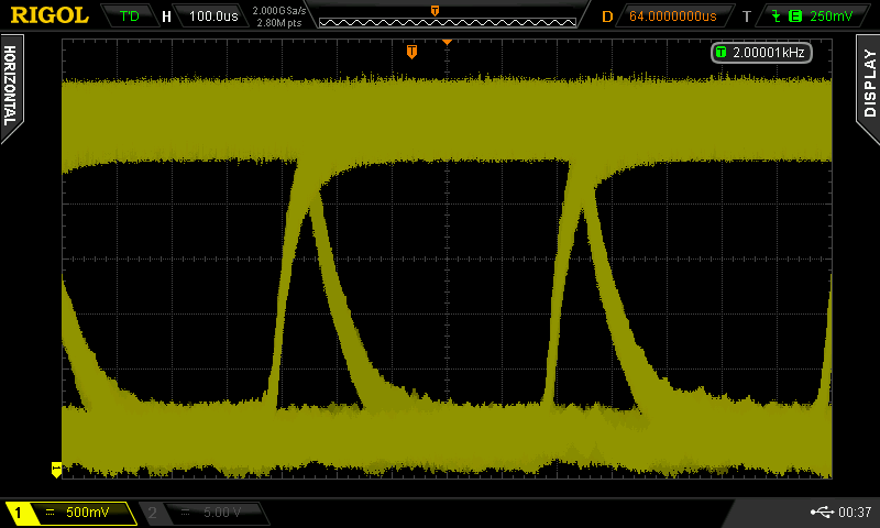
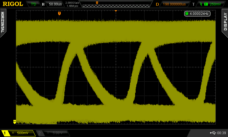
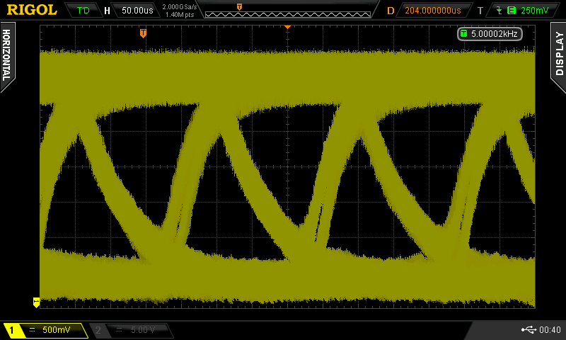
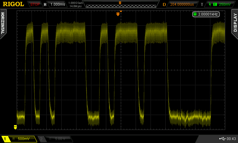
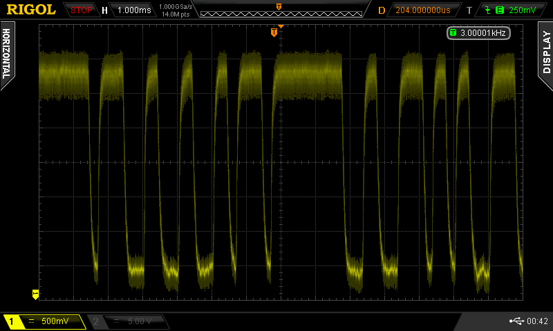
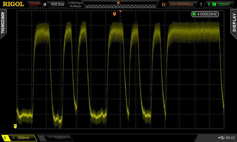
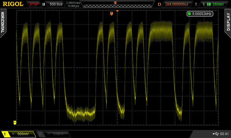
Unfortunately, because of the pure-noise power supply, the waveforms have a pretty good chance of ending up anywhere in a thick band around high or low levels. This prevents the intensity grading on the scope from producing the nice eye diagrams you may be used to seeing. With care, these are usable, though. Up to 3 kHz, the eye looks pretty good. By 4 kHz, it's getting a little tight, and by 5, some of the negative-going edges no longer make it to the bottom.
To get a better feel for the results, I also looked at the self-triggered PN bitstream:
![]() 1 kHz
1 kHz
![]() 2 kHz
2 kHz
![]() 3 kHz
3 kHz
![]() 4 kHz
4 kHz
![]() 5 kHz
5 kHz
You can really see where there's just not enough time for the negative-edges to fall at 4 and 5 kHz. Adding extra loads to the output actually increases the speed by accelerating these edges.
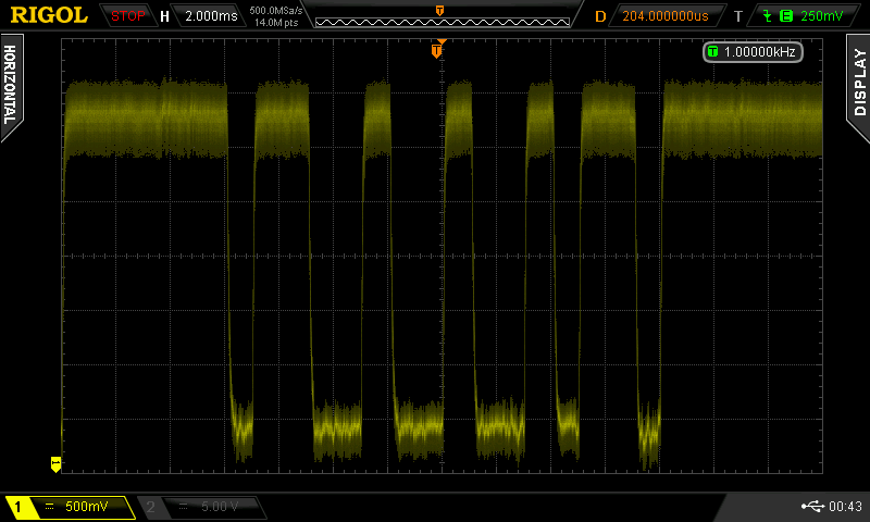
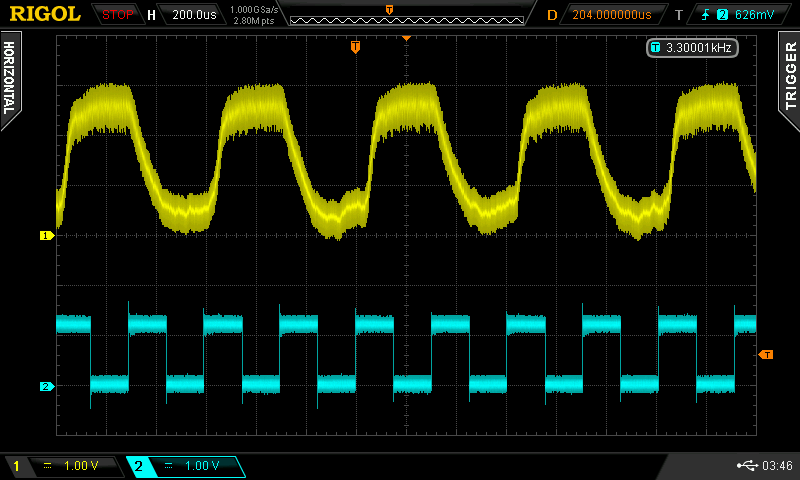
Flip-flop Toggle Speed
The second test I can use to evaluate new components in DDL boards examines how fast we can toggle a flip-flop. As shown in the schematic, the D-flop is wired to divide the incoming clock by two.
![]()
Triggering is awkward with this setup. Ideally you'd trigger on the DDS output, but then the phase of the flip-flop output is random, and you end up with a kind of eye diagram. If I had another DDS channel free, I could set that to half the f0 frequency and trigger on that, or I guess I could wire up a 74x74 to divide the clock for synch. By adjusting the scope holdoff, I was able to capture the following without too much difficulty:
![]() 1 kHz
1 kHz
![]() 2 kHz
2 kHz
![]() 3 kHz
3 kHz
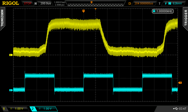
![]() 3.3 kHz
3.3 kHz
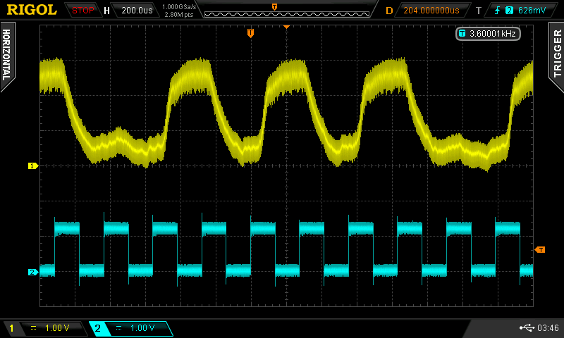
![]() 3.6 kHz
3.6 kHz
These measurements are in good agreement with my earlier and less organized results that ended up in the datasheet. The flip-flop reliably divides the input frequency up to about 3.3 kHz (which I listed as "typical"). 3.4 is also OK, but by 3.5, occasional glitches are noticeable. By 3.6 kHz, the output routinely drops pulses as shown.
Ring Oscillators
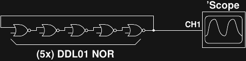
In an amazing coincidence, just last night I saw a very interesting log entry appear in my feed: Testing Propagation Delay. AlanX has been testing his discrete TTL circuits using inverter-ring oscillators on #A Discrete Transistor 7400 NAND GATE. I had never thought about doing this with DDL gates - so upon reading his post, I ran down to the lab and tried it - and it worked! Here's the test circuit I used:
![]()
The five NOR gates are connected as before, but this time, the output is connected back to the input, closing the feedback loop, and causing the circuit to oscillate. The beauty of this circuit is that it completely eliminates the input-driver issue: signals at the "input" of this circuit appear to originate from an infinite chain of inverters! Here's what the output looks like:
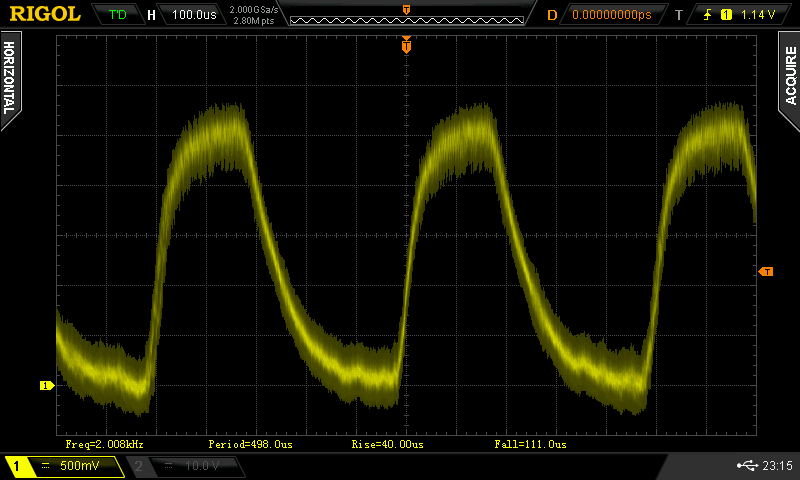
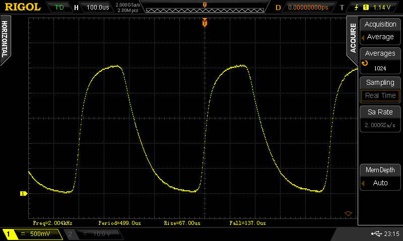
![]()
![]()
The left image uses the"sample" acquisition mode, and shows the power supply noise, as expected. On the right, the signal is averaged over 1024 samples, and provides a clean waveform for measurements. The measured frequency is 2.004 kHz (period 499 us). Assuming the H->L and L->H propagation delays are identical, this yields a 499/10 = 49.9us tpd. This is in line with the "typical" values I originally listed in the datasheet (from other measurements), but this method is much easier. The rise time of the pulses is 67us, and the fall 137us (the difference being due to the single-ended output driver of DDL gates). In total, this test gives three more data points to compare with the new components.
Next Up
The new batch of boards are arriving tomorrow, so once I populate them with the candidate components, I can run these tests and see how the substitutes perform.
Having some organized, quantitative metrics on gate performance will also allow me to revisit the design decisions involved in choosing the frequency and spectrum spreading for the power supply.
-
Control Panel
06/05/2016 at 00:02 • 0 commentsAs Seen on Hackaday
I was honored to see this project on Hackaday this past week! Thanks goes out to @Benchoff and all the fine people there for the attention and kind words.
One of the more interesting things to come out of the ensuing discussion was the "discovery" that tunnel diodes had been formed into a complete logic family in the early 1960s. I took some time to go over the patent (something I normally never do; treble damages suck), and it's pretty interesting stuff. It certainly puts to rest any debate over whether complete logic has been done with diodes before (I changed the project description to reflect this).
I was aware (from Wikipedia) that tunnel diodes had been researched for diode logic applications, but hadn't seen that they formed a complete logic family. Tunnel diodes (aka Esaki diodes) show a negative resistance region (like some other diodes used as microwave oscillators). This negative resistance region makes them useful as amplifiers, and especially bistable elements. The patent cited above uses tunnel diodes that get switched into latched states by input pulses, forming the logic gate. They also require a reset pulse before they can compute again - it's kind of like a built-in latch on the gate output. Antique tunnel diodes are available on ebay - I ordered a few to play with here, but they're expensive and pretty exotic. The kind of diode you aren't surprised you can build computers from :-)
In other news, I've created a new project for anyone interested in experimenting with "active" diode circuits. Check out #Diodes Only.
Control Panel
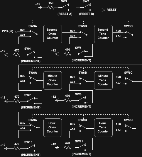
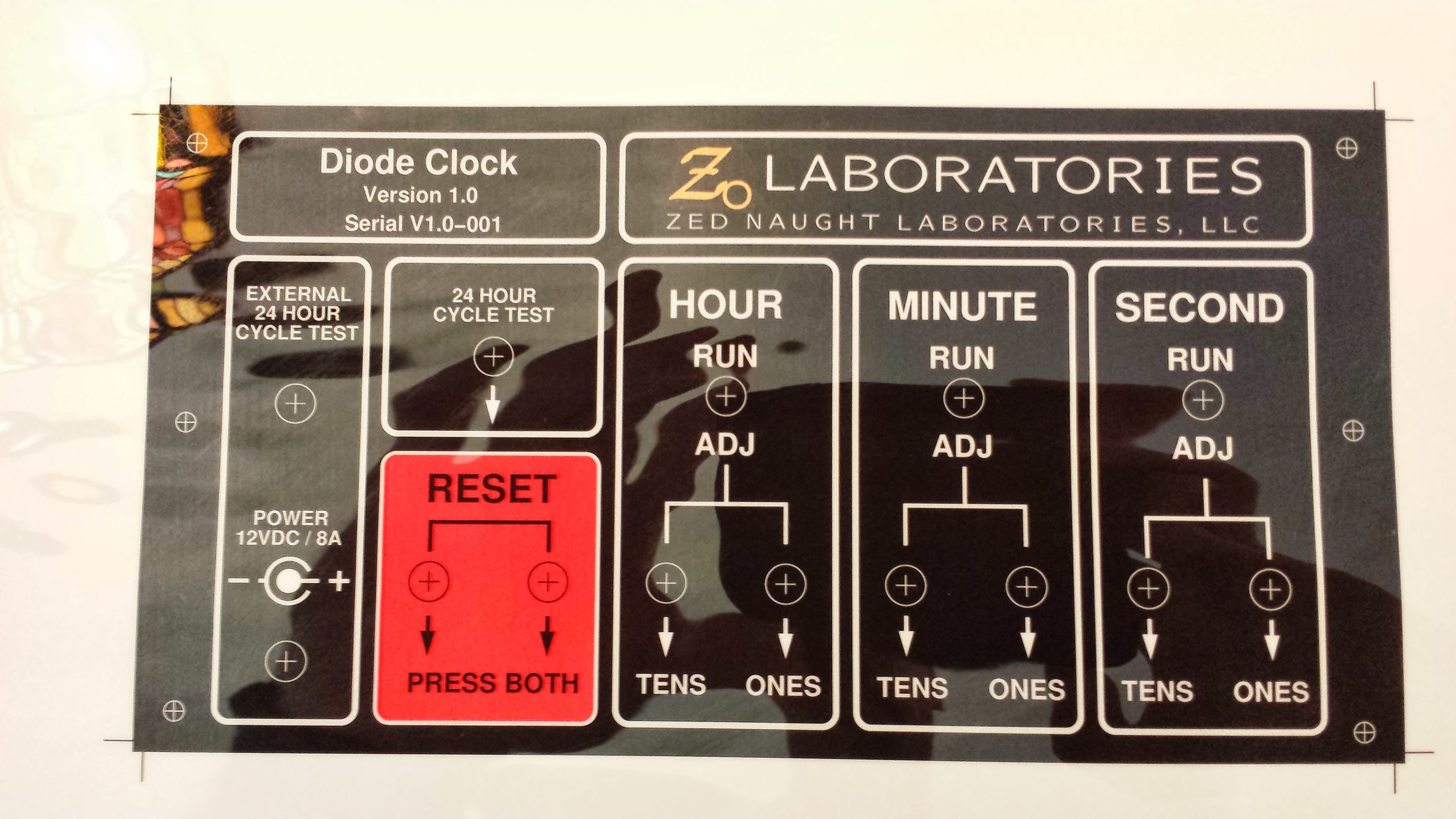
Here's the control panel for the clock:
![]()
I think it came out nice (except for the messy threadlock compound that smeared on the panel), but actually represents the biggest blunder I made with the design. See if you can figure out why from the schematic:
![]()
(here's a PDF version). The idea is to be able to isolate each digit counter with triple-throw switches on the input and output pulses, then increment a selected digit with a momentary toggle. With logic this slow, there's no need for switch debouncing, right? Turns out this was a bad assumption. During testing, things seemed to work OK, but as it was all put together, an "audience detector" somehow got incorporated. The clock becomes impossible to set if anyone is watching me do it - the switches start to bounce, and getting a digit set correctly can be frustrating. I always manage to get it to work after a few minutes fiddling, but it really bothers me.
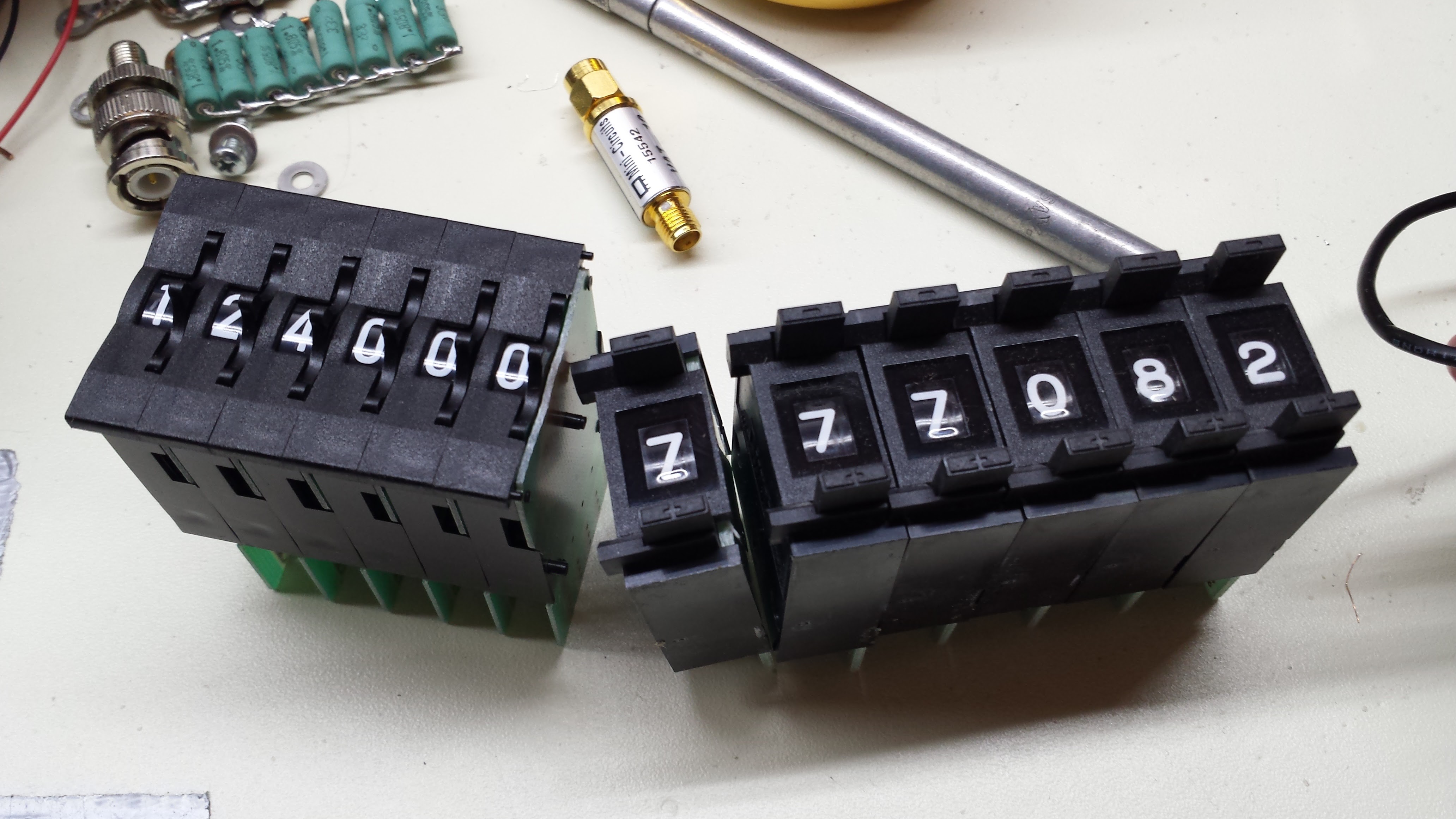
As a result, I'm designing a new panel, using thumbwheel switches, like these:
![]()
I love thumbwheels. They have a wonderful retro charm like Nixie tubes. The idea for the panel is simple - you dial the desired HH:MM:SS into the switches, then press a "set" button. The clock resets to midnight, then races forward at 3kHz seconds until it hits your appointed time. I'm considering two implementations. In the simplest, the PIC microprocessor in the timebase reads the switches and generates the reset signal and the correct number of 3kHz clocks to set the time. The advantage with this method is that the PIC can compensate for the elapsed time required to advance to the desired setting. If you're setting it to 12 noon, it's actually 12:00:14 by the time you get there, so you want to go past the set time a little to compensate. This is easy to implement on a micro. The second option is to do it all with diodes, where such automatic compensation would probably be impossible withoud adding more gates to the clock. Of course, you could require the user to pre-compensate the time before setting, which would make it a bit of a puzzle to set. I haven't decided which way to go yet.
Making Nice Panels
I use a process for panel labels that I learned from the website of Neil Heckt, who was the owner of Almost All Digital Electronics. In preparing this update, I was sad to learn that Neil passed away in 2015. I've used one of his L/C Meter IIB units for many years, and throughout the development of this clock. His idea was to laser-print labels on the back of transparency sheets and glue them to panels. It works really well.
Here's what I did. I designed the blacked-out label (in xfig), then mirrored it for printing on the back of the sheet. I used a color laser printer so I could also get the red for the reset box. To get the metallic gold logo, I left the area clear, then spray-painted it from the back with metallic paint (the photo doesn't do it justice). I then spray painted the whole back of the panel with white to form the lines and text. Once it was dry, I flipped it and sprayed a light coat of matte finish to take down the shine on the front (glaring in the photo below). I attached the label to the pre-punched aluminum panel with spray adhesive, then cut out the holes with an X-ACTO blade.
One mistake I made was not using panel washers under the nuts. This caused the nuts to grab the transparency and warp it a little. To avoid having to torque the nuts so much, I applied some thread locker to keep them tight, but this got on the panel in places and marred the finish. In retrospect, I think a two-panel arrangement where the switches are mounted to a rear aluminum panel with a labeled faceplate applied after the nuts would have been better.
![]()
-
End to End Power Supply Tests
06/03/2016 at 21:03 • 0 commentsWhy Bother?
You might wonder why I'd bother spending so much time worrying about EMI from the clock. There are basically two reasons. First, I want to be a good RF citizen. In my astrophotography hobby, I'm constantly battling light pollution, so I understand the impact of unwanted photons. I'm slightly less involved with amateur radio, but I've seen the problems of RF noise there, too.
The other reason for concern is that I would like to stay out of trouble with the authorities. In the US, the FCC enforces rules concerning EMI. I believe 47 CFR 15.23 covers this situation:
§ 15.23 Home-built devices.
(a) Equipment authorization is not required for devices that are not marketed, are not constructed from a kit, and are built in quantities of five or less for personal use.
(b) It is recognized that the individual builder of home-built equipment may not possess the means to perform the measurements for determining compliance with the regulations. In this case, the builder is expected to employ good engineering practices to meet the specified technical standards to the greatest extent practicable. The provisions of § 15.5 apply to this equipment.The 15.5 section they refer to basically says that you can't operate your device if it causes harmful interference, or if the FCC notifies you that you must cease. I won't ask anyone to comment on whether I observe "good engineering practices" :-)
Test Results
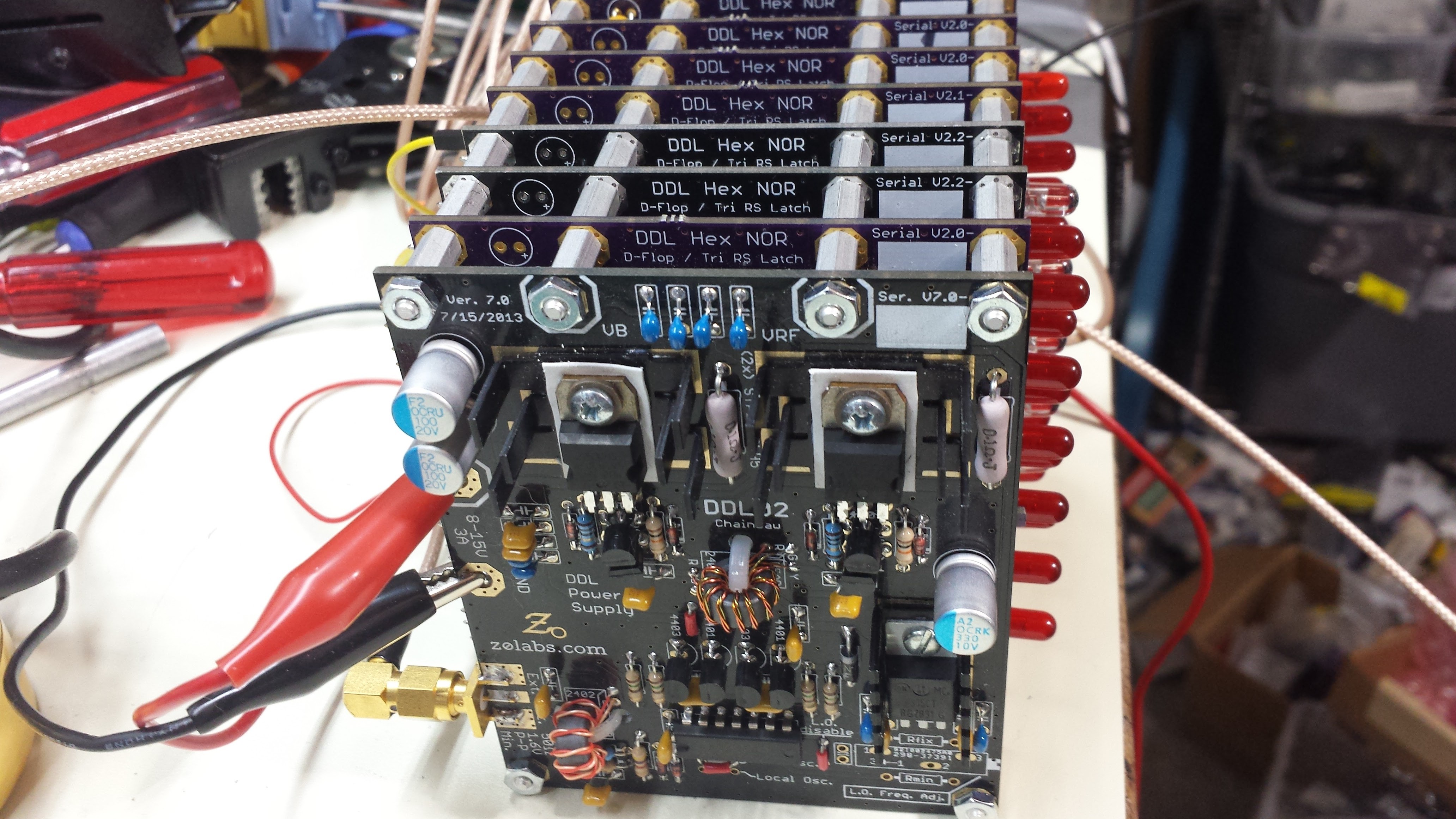
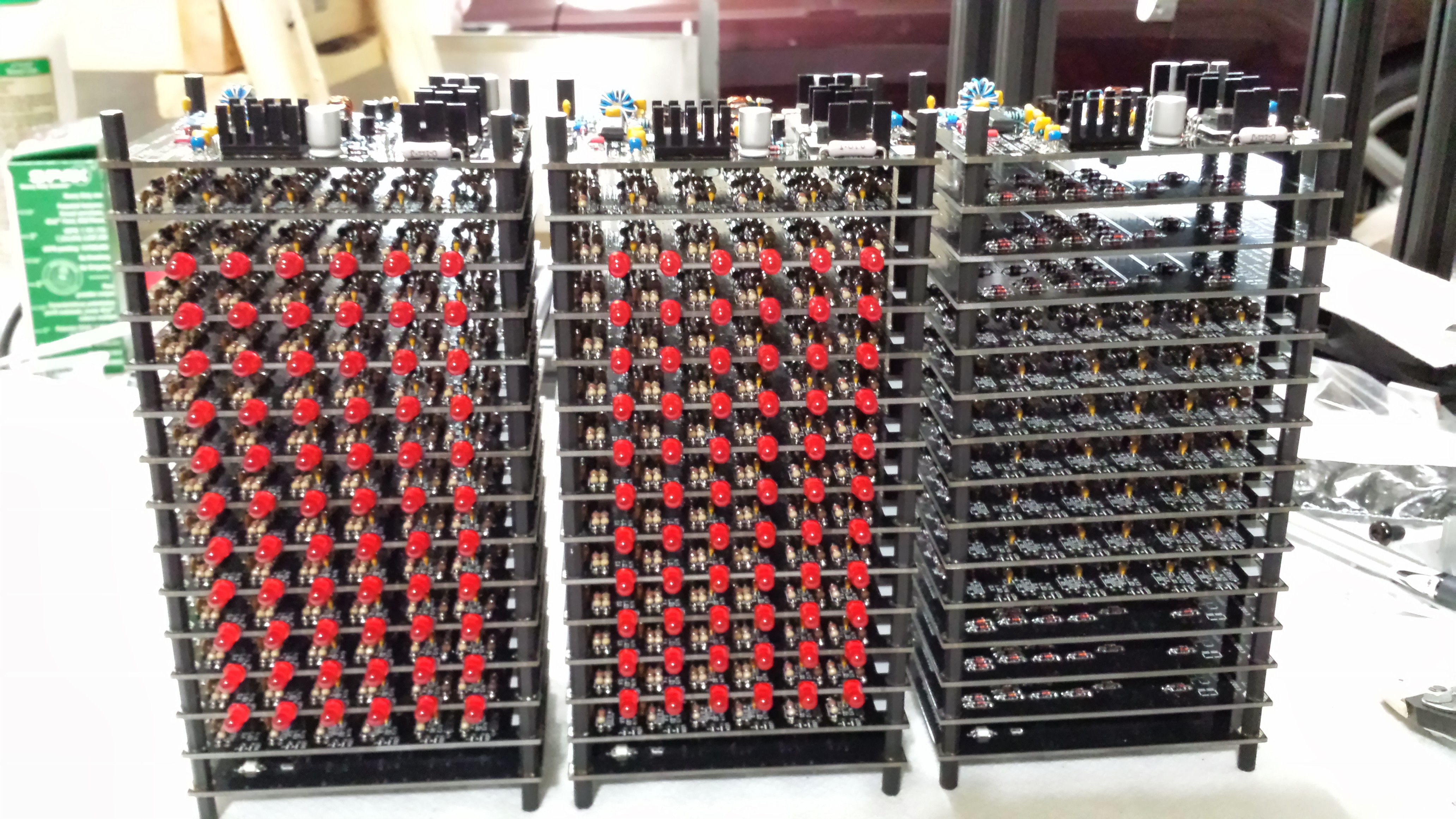
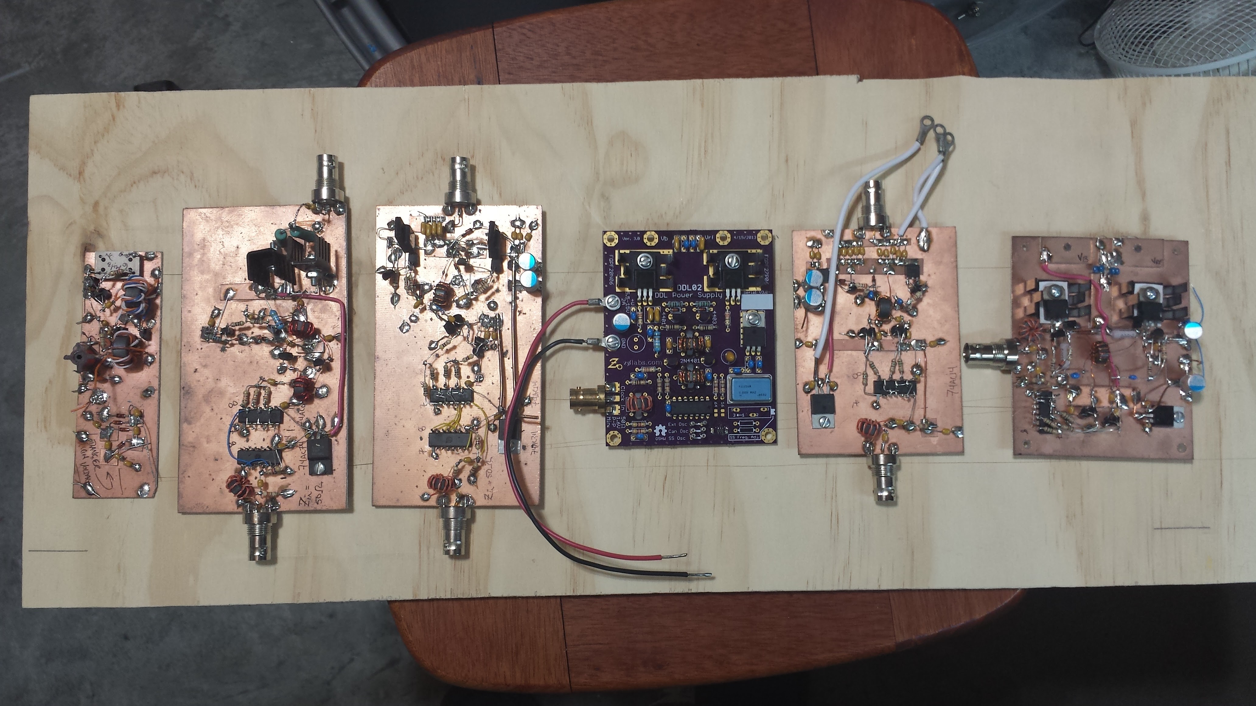
I finally had some time to collect some data on the power supply end-to-end. For all these measurements, I used a stack of seven DDL01's (various 2.x versions) and a DDL02 power supply, shown below. All measurements were taken between the Vrf and ground connections, i.e., the standoffs in the upper right. In each case, measurements were taken at three points along the stack: at the power supply board, after the fourth board, and after the seventh (including standoffs protruding from the back of the last board).
![]()
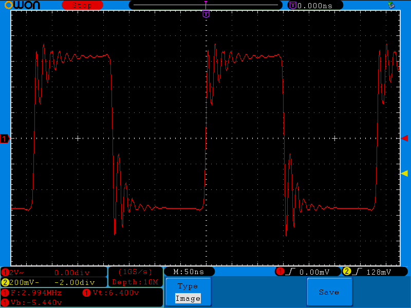
3 MHz Clock, Time Domain
Here's the output in the time domain. At the power supply end, we can clearly see the VHF ringing as was seen driving the resistive dummy load. Interestingly, though, the ringing is diminished substantially as we move along the stack. By the seventh board, it is all but gone.
![]()
![]()
![]()
At DDL02 Supply After Fourth board At End of Stack This puzzled me for a while: intuitively, I thought the inductance of the standoffs should be low enough so that the supply would be essentially unchanged by a reasonably long stack of boards. The problem is that my intuition has been shaped by years of playing in the 50-ohm world; things are very different here in the milliohm region.
Allow me some "spherical cow" calculations. Let's treat the Vrf and ground standoffs as a short parallel transmission line, which is nicely modeled as an inductance. The standoffs are 5mm diameter (hexagonal, but assume round), 11mm long, and 19mm apart. A web calculator estimates the inductance of these parallel lines as about 8.9nH. At 3 MHz, this yields an impedance of 0.17 ohms, which would indeed be negligible in a 50-ohm system, but is really significant compared to the 0.13 ohm output impedance of the DDL02.
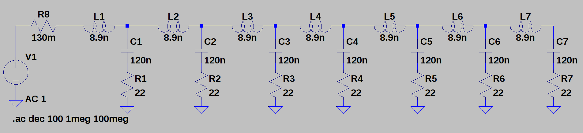
In case the cow wasn't quite spherical enough, let's further model each DDL02 board as a single 120 nF capacitor in series with a 22 ohm resistor (there are six gates on the board, each with a 10nF capacitor to a each of a 330 and 220 ohm resistor - it's a very rough model, and ignores any "off" diodes and the board layout entirely). Assuming this, we can model the stack of boards as a multi-section RLC filter. For convenience, I've lumped all the inductance into one inductor at each stage - the reality is a bit more complicated. Here's the over-over-simplified LTspice model:
![]()
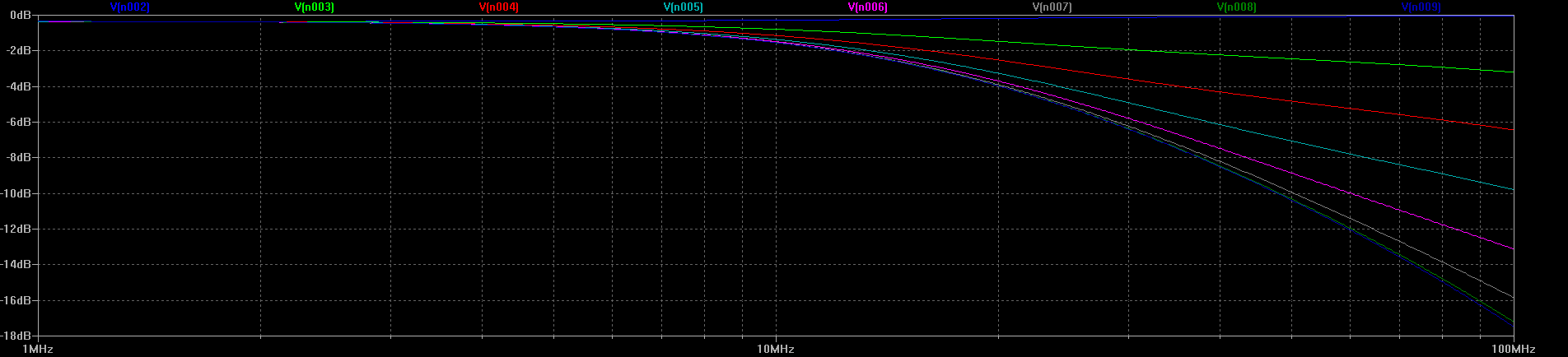
and the associated Bode plot:
![]()
It turns out that using standoffs for bussing RF to the boards has formed a nice low-pass filter, reducing the harmonics most likely to be radiated from a structure this size. I wish I could take credit for this, but it was pure accident.
I guess one could divide the measured spectra at the various points (shown below) to estimate the actual response. Maybe I will collect the data to do this after some more of the documentation is complete.
Frequency Domain
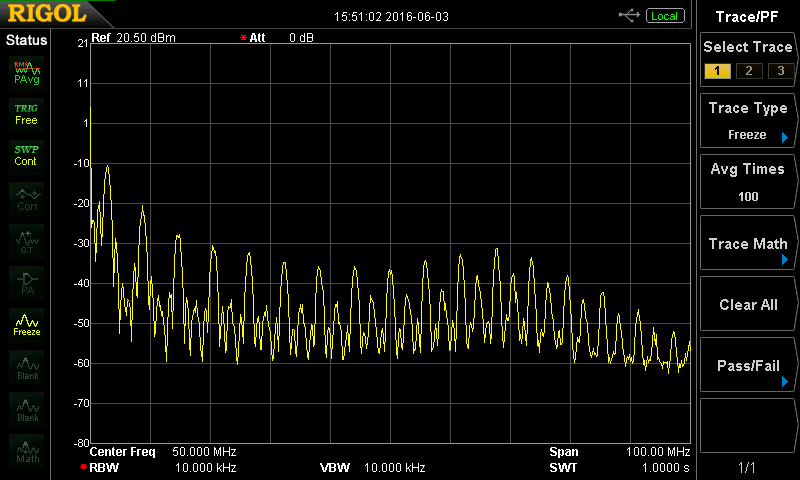
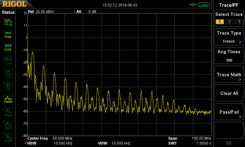
For the frequency domain plots, I switched to using the DDL04 as input with the usual 3-divider for the bandwidth spread setting. A look at the spectrum to 100 MHz shows the VHF frequencies between 60 and 70 MHz are decently attenuated by the accidental filter:
![]()
![]()
![]()
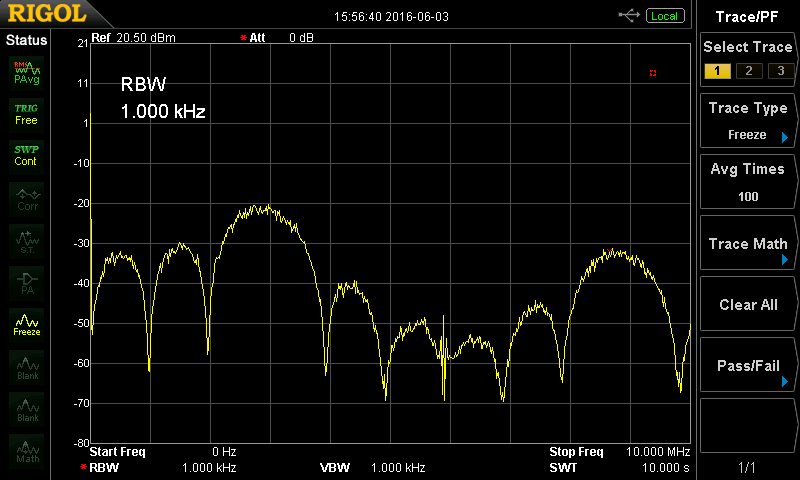
At DDL02 Supply After Fourth board At End of Stack Finally, a look at the spectrum to 10 MHz shows output similar to that of the DDL04 alone:
![]()
It's important to remember that the values plotted (in dBm) here assume a 50-ohm system impedance. In a fully-loaded DDL02 with a load impedance of around 1 ohm, the actual power would be about 50 times (17 dB) greater than reported.
What does it mean?
Not too much. To really evaluate the potential for radio-frequency interference from the DDL system components, we'd have to measure low-frequency emissions back into the power supply using a LISN (line-impedance stabilization network), and higher-frequency emissions with a calibrated antenna in an anechoic RF environment. I don't have access to any of that stuff, so I ran some simple tests. With a portable receiver, I tested reception of several shortwave stations, including one in the vicinity of the 9 MHz lobe of the above spectrum. Within about a meter of the 7-board stack, the interference was pretty strong and clearly mechanical sounding. By the time I had walked to the other side of the house, however, it had faded into the noise floor (although it's possible the noise floor itself had been raised).
The bottom line is that I'm not too worried about emissions from these devices at the moment - I just don't think it will be a problem. If I do end up interfering with something, I'll shut it off and revisit the issue.
Next up: I got a heavy box of goodies from DigiKey yesterday, including alternative ferrite cores to test, as well as (10) 1N4007s from every manufacturer they carry. I'll run some tests to see if there are any "duds" in this application. My suspicion is that they'll all work fine...
-
DDL04 Spread Spectrum Exciter [Part 2]
05/26/2016 at 01:45 • 0 commentsTime Domain
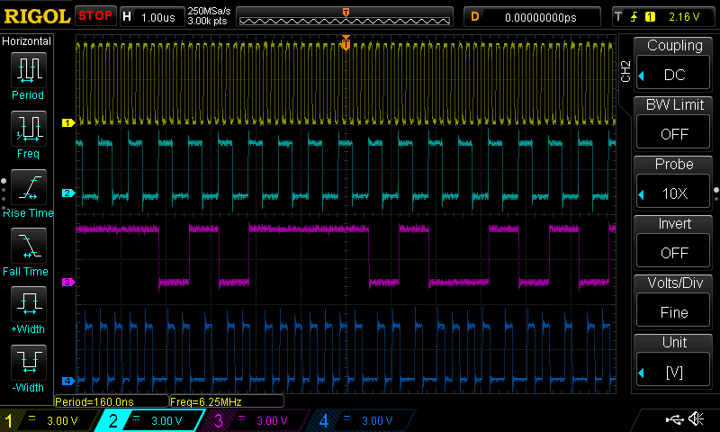
To verify the operation of the DDL04, I first looked at the signals in the time domain:
![]()
The traces are as follows:
- (yellow) : 6MHz clock input
- (cyan): Divider output (set to "2")
- (magenta): LFSR output (pseudo-noise bit stream)
- (blue): Spread-spectrum output
Everything seems reasonable here. The bandwidth divisior is set to 2, so the divisor output is the base clock / 4 (there's always a fixed 2x divisor). The pseudo-noise looks pseudo-noisy, and the output certainly looks modulated by it, but the time domain isn't the best place to analyze the output signal.
Frequency Domain
To examine the signals in the frequency domian, the output was connected to a spectrum analyzer through a 20dB external attenuator. Just in case. Nothing ruins your week like blowing the first mixer in your SA (trust me). At least this one beeps when it's over-driven.
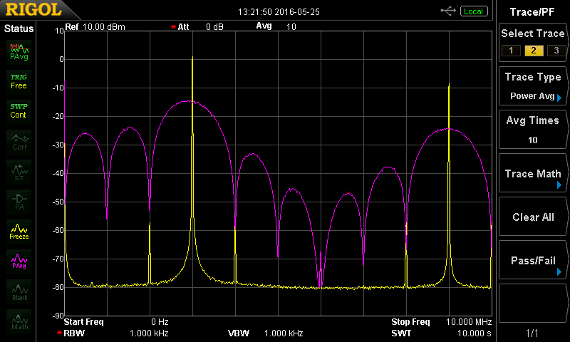
In the image below, the yellow trace is the non-spread signal (fundamental at 3MHz). The approximately -60 dBm sidebands at +/- 1 MHz are spurs from the DDS generator I used to drive the board at 6 MHz. The magenta trace is the output of the board spread with a 2-divider (+/- 1.5MHz at first zeros). Seems like it's working.
![]()
There's an important note about this kind of comparison. It would be tempting to compare the peaks at 3 MHz and conclude that the spreading has reduced possible interference by about 15 dB. While this kind of analysis works for narrow-band signals, noise (even pseudo-noise) is a different animal. The measured amplitude of a noise signal depends on the measurement bandwidth: in these plots, the analyzer has been set to a resolution bandwidth of 1 kHz. Measuring using a wider bandwidth will move the magenta curve upward; a narrower bandwidth will move it down. Likewise, in a receiver, the amount of interference received will depend on the reception bandwidth.
Another point of interest. Although the curve appears continuous, it is actually composed of 32767 individual spikes, in this case spaced at 1.5 MHz / 32767 = 45.8 Hz. The narrowest RBW on this particular analyzer is 100 Hz, so it can't resolve these spikes.
Here's the same image with the divider set to 3 (3 +/- 1 MHz inside the central lobe). This is the setting that seems to work best with the clock as-built. I would have liked to use the widest bandwidth setting, but the DDL gates don't perform as well with the lower-frequency energy in that signal. I suspect the ideal approach is to use maybe a 9 MHz clock with the 2-divisor, yielding a 4.5 +/- 2.25 main lobe, but I haven't had time to do an in-depth analysis.
![]()
For completeness, here's the output with the divisor cranked all the way to 10 (yes, I did think about having it go to 11, but it's not easy using a '4017). This is a pretty narrow bandwidth, and is probably only useful for diode gates using tuned circuits, quarter-wave lines, or other narrow-band structures.
![]()
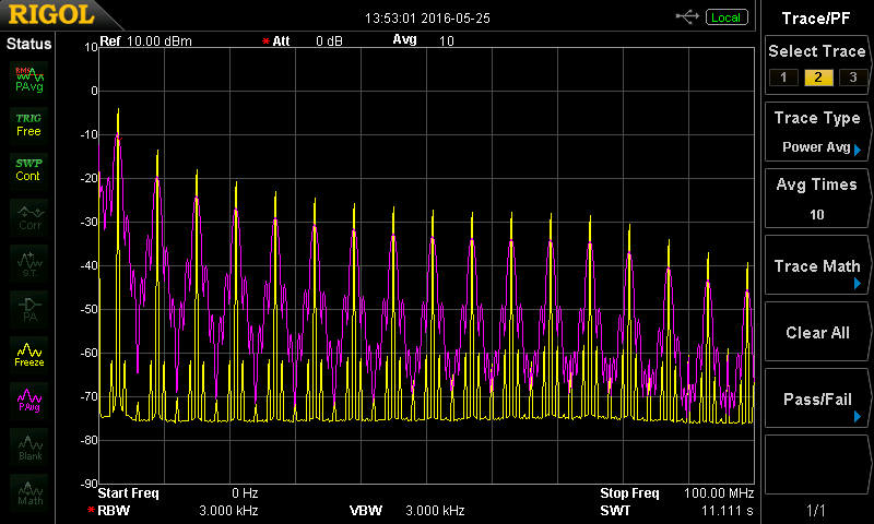
Finally, a quick look further up the spectrum (here to 100 MHz) shows what we'd expect - the fast edge rates on the 74AC244 contain strong harmonics into the VHF region. Of course, at the output of the the board, this signal is still just logic-level (and inside coax) so there's not too much concern. Additionally, filtering it here would be pointless; the DDL02 will just restore the hard edges and the corresponding harmonics (it is by no means a linear amplifier). In the sequel, I'll measure the power supply system end-to-end.
![]()
Next: Puzzling measurements and 4-40 threaded standoffs as inductors.
-
DDL04 Spread Spectrum Exciter [Part 1]
05/25/2016 at 03:39 • 1 commentDesign
The diode clock uses four radio-frequency power supplies. To reduce emissions, they are driven with a spread-spectrum signal produced by the DDL04. The spectrum of this signal is tuned to give good performance with DDL V2.x logic boards. Here's a simplified schematic (5V power supply components omitted):
![]()
Since it's an eye chart on this page, here's a pdf version.
The goal is to provide a spread-spectrum clock with a selectable spreading width around an input clock source. To do this, a variable divider clocks a 15-stage linear-feedback shift register (LFSR) producing a pseudo-random bit stream. This bit stream then modulates the original clock signal to spread the spectrum, which is output through coax to the four DDL02 power supply boards. Two opposing clock phases are produced by the board, so that adjacent DDL stacks can be clocked 180-degrees out of phase, (theoretically) reducing RF emissions.
The system is clocked by a standard oscillator "can", nominally 6 MHz, although something around 9 or 10 MHz might be a better choice for DDL V2.x - more on that later. A 74AC74 flip-flop divides the crystal frequency by two. A 74HC4017 decade counter combined with dip switches and a diode-OR gate allow a programmable divisor between 1 and 10, effectively setting the clock spreading width. A 15-stage LFSR constructed from a pair of 74HC164s produces a pseudo-noise bit stream based on the output of the '4017. Although the shift-register is long enough for a 16-bit LFSR, an extra XOR gate package would be required on this board to implement the feedback. The 15-stage LFSR outputs a stream of (2^15 - 1) = 32767 pseudo-random bits before repeating.
The output of the LFSR is used to selectively invert the original clock signal in another XOR gate, effectively modulating it by the LFSR's spectrum. The net result is a spreading width that is an integral divisor of the original clock frequency. The remaining 74AC74 flip-flop is used to synchronize the modulated clock, preventing runt pulses which wouldn't make it through the DDL02 power supplies.
The output driver is a 74AC244, with each 50-ohm jack driven by two gates. 74AC logic has symmetrical output impedance of around 12 ohms. An 86.6 ohm resistor in series with each output raises this to approximately 100 ohms, and two such outputs paralleled provide a good match to 50-ohm cable and enough current to drive it.
LFSR Watchdog
The combination of D5/C7/R6 deserves a quick mention. It functions as a crude "LFSR watchdog", re-starting the LFSR should it ever become "stuck." The LFSR has only one forbidden state: a register full of zeros will remain full of zeros. Unfortunately, that's exactly the state that the /CLR line puts the 74HC164 into, and being a serial-in, parallel-out register, there's no way to jam some initial state in "from the side." Using a power-on reset would require clocking in some non-zero initial state. The LFSR watchdog implemented here takes a different approach, sampling the bits as they move through the register. As long as there are some ones shifting though, D5 keeps C7 charged, and the associated Schmitt-trigger inverter output low. Should a long-enough string of zeros occur, C7 will discharge through R6, the inverter will flip and start inverting the feedback to the register, pumping in ones to restore a valid state. As soon as the ones start circulating again, C7 gets charged back up, and the feedback polarity is restored. Since the LFSR can output at most 14 consecutive zeros in normal operation, the RC time constant is easily chosen to avoid false-triggering, but quickly detect a stuck state.
Substituting Parts
Because of the low speeds involved here, I used 74HC and 74AC parts interchangeably. The notable exception is the 74AC244, which is used to drive four 50-ohm coax lines. An HC can't handle the currents involved, so don't substitute. All the parts except the 74HC4017 are also made in a 74AC version, so if another dividing mechanism is used (like a 4-bit loadable counter), this circuit could be used with much higher clock speeds.
Noise Period
The LFSR uses a maximum-length feedback polynomial:
which has a period of 32767 clock cycles. The bandwidth of the central spectral lobe and the pseudo-noise repeat period are determined by the spreading divisor setting. One of the design goals was to have the noise repeat period in (or close to) the infrasonic range to reduce the probability of detectable interference if any EMI did leak from the clock. This table shows some of the settings (others omitted for brevity) for a 6 MHz crystal oscillator.
Clock Divisor Central Lobe Bandwidth Pseudo-noise repeat frequency 1 XTAL oscillator BW NA 2 3 MHz 46 Hz 3 2 MHz 30 Hz ... ... ... 10 600 kHz 9.2 Hz Design Files
The Eagle design files are shared here, and boards can be ordered at OSH Park.
I haven't put together a formal BOM yet - I'm going to make one for this as well as the three flavors of the DDL01 shortly. For now, the parts are pretty clear on the silkscreen, except perhaps "RSSD" (aka R6) and "CSSD" (aka C7) in the LFSR watchdog detector - 10k and 1n work well here.
Here's an instance of the board I populated this week to collect some data:
![]()
For testing, the crystal oscillator can is not mounted, and a coax pigtail is wired in its place (with a series resistor and a pair of diodes jammed in there for protection from ESD and over-zealous signal generators). I only soldered on one SMA jack - no sense mounting $20 of hardware just to grab some data. When I built this particular board, I forgot to populate the LFSR watchdog capacitor, CSSD (aka C7) - don't try this at home, because you'll shorten the LFSR period significantly, then waste a day or so trying to figure it out.
Next: analyzing the output in the time and frequency domains
-
Clock Display Boards
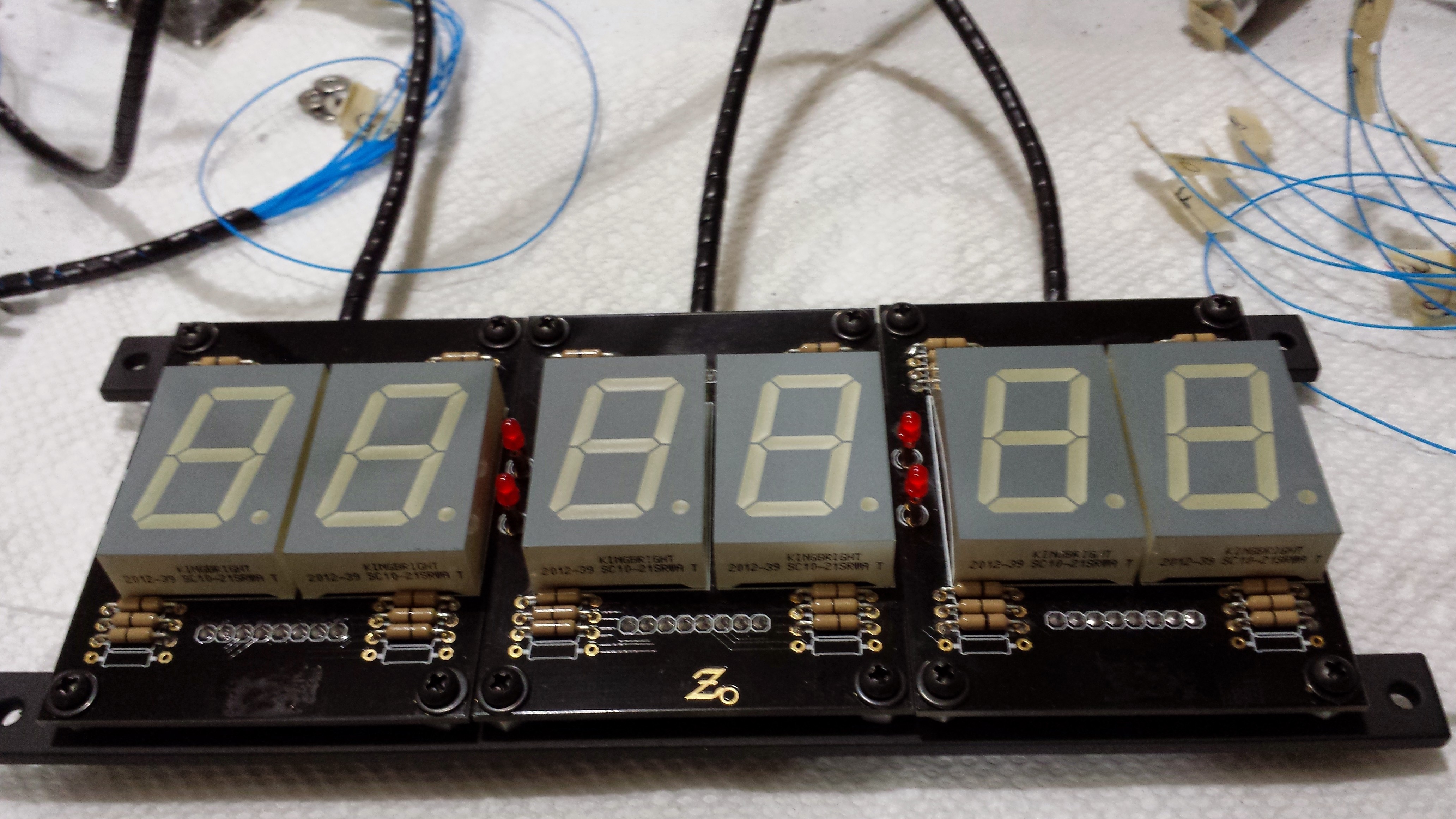
05/25/2016 at 03:15 • 0 commentsThe clock face is made from three identical boards, shown here bolted to their aluminum mounting rails. The two rightmost boards have their colon LEDs populated, while the two outer boards have the bottom backlit logo painted over (quite poorly, I might add).
![]()
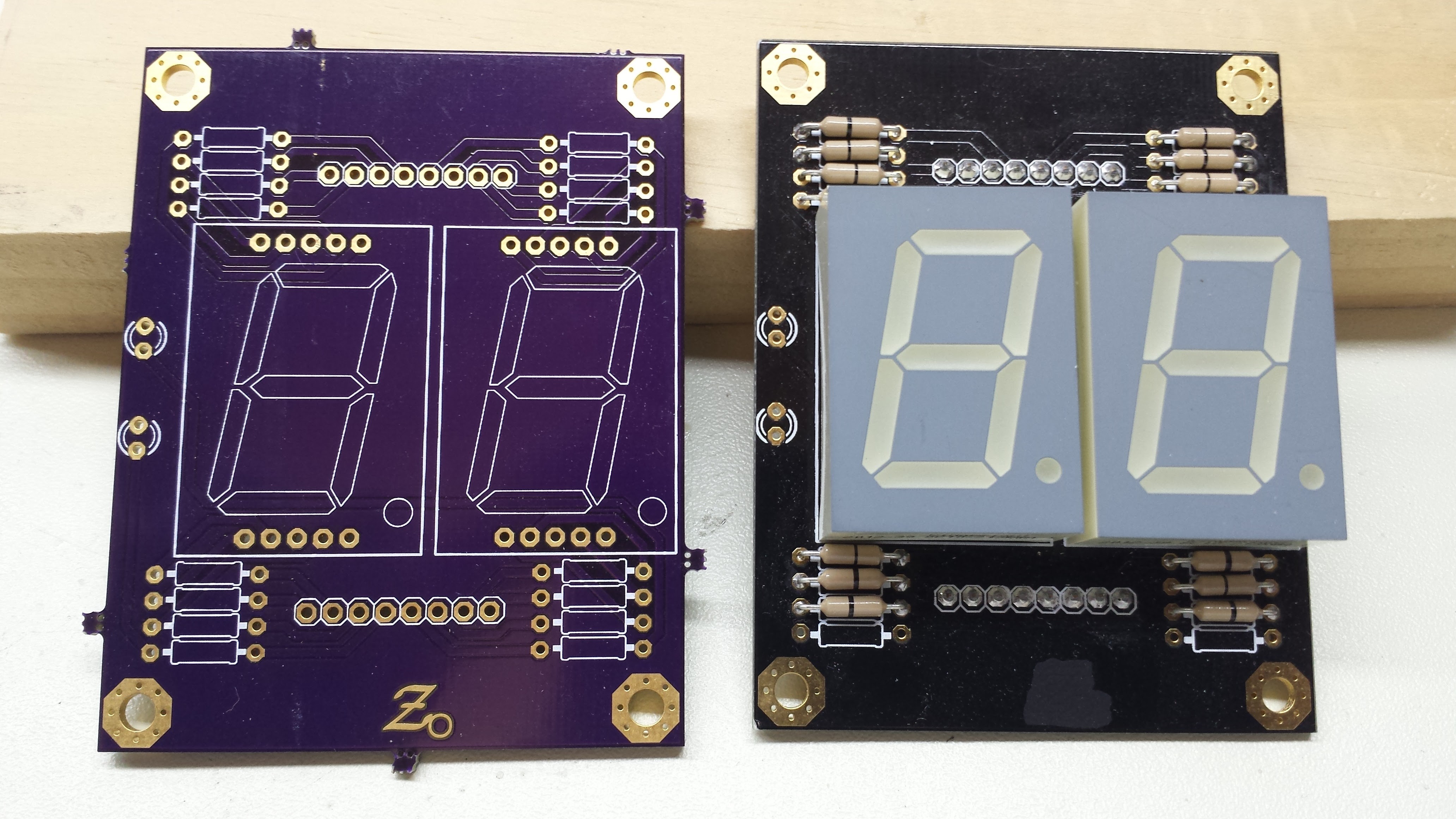
Here's a close-up. The board on the right was rejected because I soldered the displays on crooked. Tape them in place before soldering - a little folded paper in between can help keep the spacing uniform.
![]()
The "resistors" on the board are zero-ohm - when I designed the board, I wasn't sure if they'd be needed or not. As it turns out, the maximum output current of the DDL drivers (approx. 9mA) doesn't require any resistors. The unpopulated resistor sites on the bottom of the board are for the colon LEDs. When I assembled the board, I wasn't sure what values would be required to match the brightness of the colons to the displays. I determined this experimentally after the clock was up and running, and spliced resistors into wires running from the timebase 5V supply to the colon LEDs.
Header pins extend from the back of the board (soldered on the top side, directly above and below the displays).
Design Files
Gerbers are shared on OSH Park, and purple boards can be ordered there.
Eagle design files are here on hackaday.io.
BOM
Each display board requires the following parts:
- (2) Kingbright SC10-21SRWA 7-segment display SC10-21SRWA @ DigiKey
- (14) Zero-ohm resistors (suitable ones by Yageo @ DigiKey), or use wire jumpers
- (2) 3mm LED Kingbright WP710A10SRD-D WP710A10SRD-D @ DigiKey
- Header pins as desired for connections
Don't substitute the 7-segment displays unless you verify proper operation with your intended part. These displays are ultra-bright and efficient with a low forward voltage, so they can be driven easily by DDL gates. The efficiency of the colon LEDs is less of an issue, since they're lit by the 5V rail, but these particular ones are color-matched to the displays. The colon LEDs are mounted with small standoffs to match the height of the displays. I cut some pieces of tiny copper tubing to slip over the leads as spacers, but anything similar would work.
Next: DDL04 Spread Spectrum Exciter (and EMI tamer, hopefully)
-
DDL02 Power Supply [Part 2]
05/22/2016 at 16:39 • 0 commentsDDL02 V7.1
See Part 1 of this log for details of the power supply circuit.
Gerbers
I started sharing the DDL02 V7.1 gerbers on OSH Park. V7.1 has an updated silkscreen and schematic with designators that match the other design files. In addition, designators are now on the silkscreen, so you know what to put where. After doing my own projects for so long, I got in the bad habit of not labeling the components very well. I'm trying to reform. Electrically, the board is identical to the V7.0 version I used on the clock.
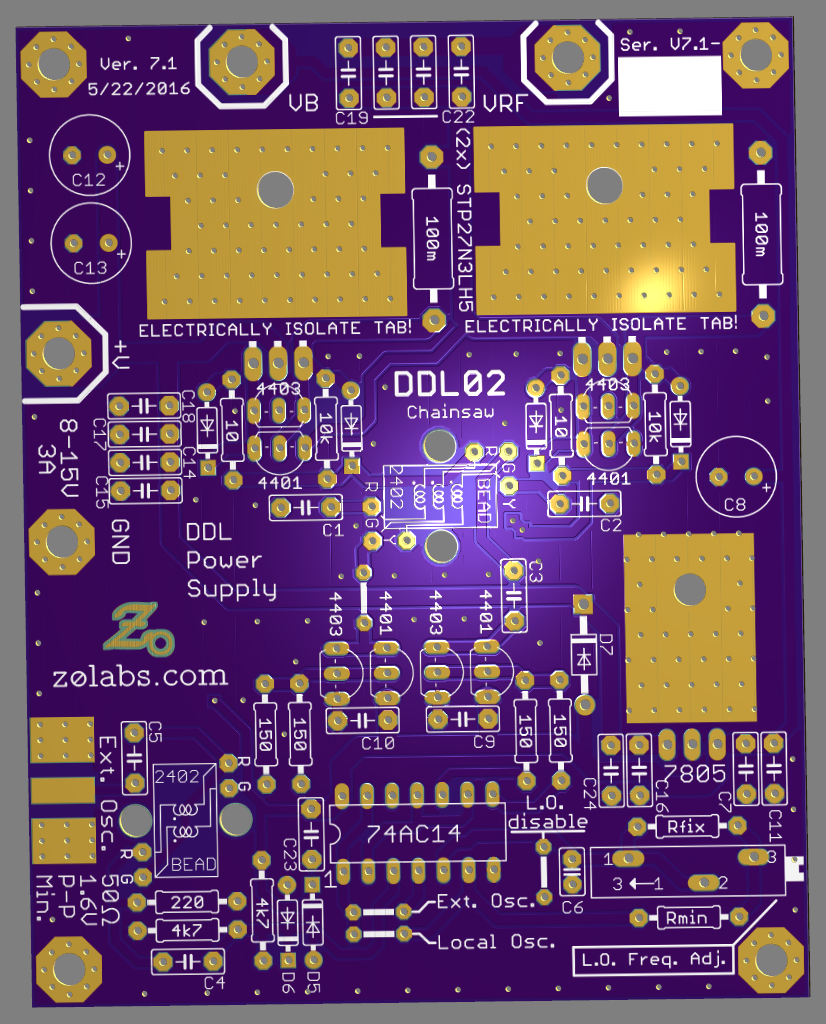
Here's a render of the new version that I made using my in-house pre-flight 3D gerber previewer. This previewer software is on my list of things to open-source:
![]()
BOM
In the same spirit, I've created a detailed BOM for the DDL02. It's a google docs spreadsheet shared read-only (licensed CC-BY-SA). For some reason, formulas won't calculate for me - probably something to do with the privacy settings on my browser - so I couldn't make it quite as nice as I wanted. Once I get google docs working properly, I can revisit. I'd welcome any feedback on the BOM - I intend to make similar ones for the other boards, and would like to improve as I go.
There is one item on the BOM I'm not certain of yet. I wound the original transformers on Fair-Rite 2643002402 beads, and listed here the Laird 35T0501-10H instead so builders could order from one distributor. I haven't tested transformers on the Laird cores yet, but I'm waiting for some now, and will post an update once I have. The transformer windings should be bifilar (T2) and trifilar (T1) wound to reduce leakage inductance - you can find good tutorials on the web if you haven't wound one before. It's easy and rewarding: not too often do you get to make your own components.
Try not to substitute capacitors with lower voltage ratings. You might think that 50V caps in a 12V circuit are unnecessary, but ceramic caps have a nasty habit of exhibiting reduced capacitance as the voltage across them increases. If you substitute 16V caps instead, you may find a chunk of your capacitance has disappeared.
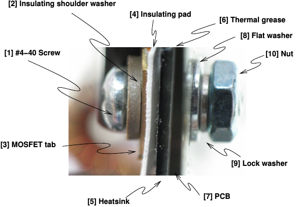
Q1 and Q2 must have their tabs isolated from the ground plane on the PCB beneath them. Here's the heatsink assembly as I built it:
![]()
4-40 (or M3) hardware fits.
Design files
The Eagle design files are shared on hackaday.io.
Testing
OK, you built your first DDL02. Congratulations! Now, how do you know it works?
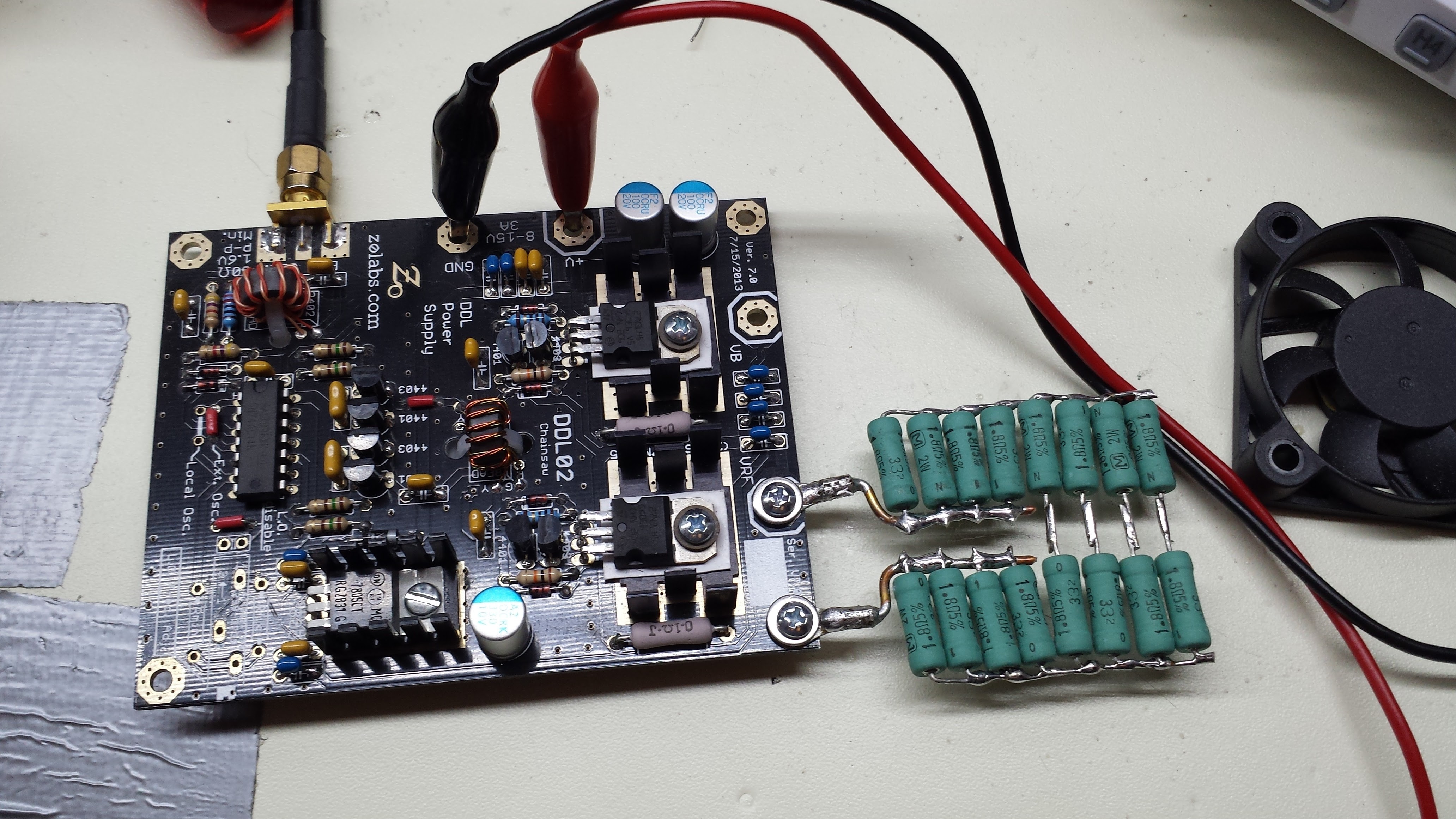
Here's what I did. I happened to have a bag of surplus 1.8 ohm 2W metal oxide resistors: 1.8 ohms is in the correct range to verify proper operation of the power supply. Unfortunately, a 2W resistor dropped across this power supply wouldn't last very long - so I made a 1.8 ohm 32W resistor using 16 of them. You could also use carbon composition resistors for this, but avoid wire-wound resistors of any type - they have far too much parasitic inductance. I run the fan over the resistors for longer tests. You can also test the supply with a stack of DDL01's, if you have them around.
![]()
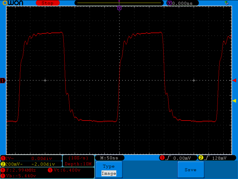
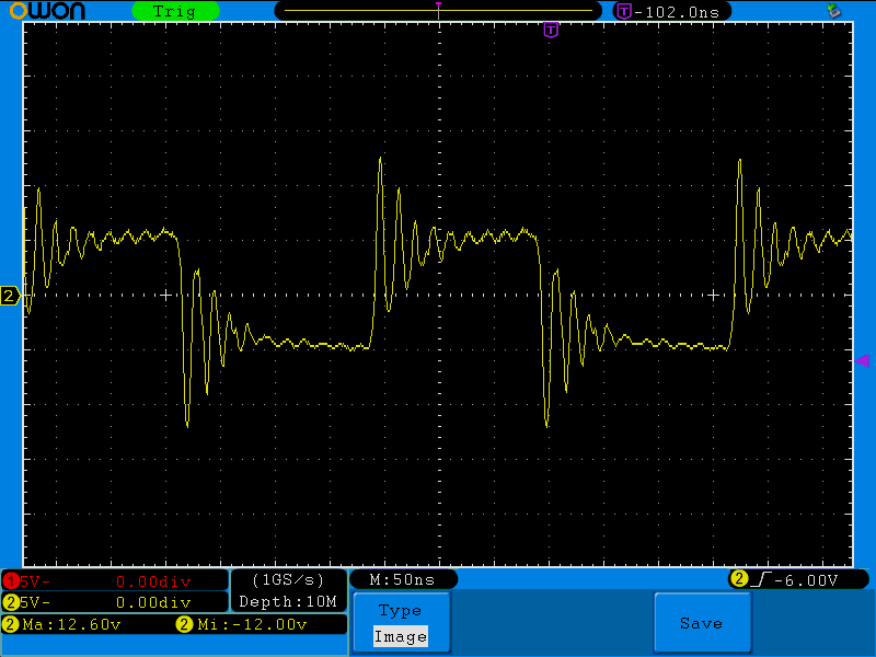
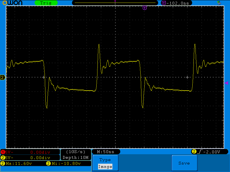
For testing, I initially started the "12V" supply at around 7.5 (a little above the 7805's dropout), and watched the current draw carefully as I proceeded. If you have a current-limited lab supply, this is the time to use it. I drove the input with a 3MHz +7dBm source ("TTL" output from a signal generator will work well), and slowly increased the supply to 12V. Current draw for this load at 12V and 3MHz is around 0.7A . Using a 10x oscilloscope probe on a 100MHz scope, you see the following output:
![]()
That ringing isn't bad probing - you see the same thing with a Z0-probe into a terminated scope input. Ringing like this is common with very fast MOSFET driver circuits (especially on through-hole PCBs - and on those designed by amateurs :-) The cause of and solutions to this problem are well-explained by Ti Applicaton Report SLPA010 "Reducing Ringing Techniques for NexFET High-Performance MOSFETS". There are two possible concerns here. First, the ringing excursions could exceed the Vds rating of the MOSFETS - in this case, the 24Vp-p excursions are within a safe margin for 30V MOSFETS. The second concern regards emissions. A quick look at the ringing shows it to be around 60MHz. While the size of the conductors in the clock don't make effective radiators for the 3MHz signal here, 60 MHz leakage could be an issue.
I'll note here that the DDL01 boards don't care about this ringing; they work fine either way.
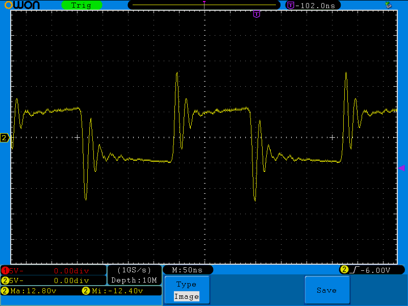
To be a better EMI citizen, we can clean up the waveform with an RC snubber. Following the design procedure outlined in the Ti document, I first tried a 100pF capacitor in series with a 13 ohm resistor across the output:
![]()
Definitely better, but still not great. I tried a few other combinations before settling on a 220pF/10 ohm snubber, which resulted in the following:
![]()
now, the initial excursion is still there, but the 60MHz energy is damped pretty well.
There aren't sites on the current rev of the DDL02 board for the snubber components - they are better off determined experimentally when the board is attached to the desired load. The series RC circuit can then just be wired conveniently across the Vrf and ground terminals on the DDL01.
Thermal Issues
For a long time, I thought the power devices ran too hot on the board. This was based on the age-old "finger test" in which the engineer sticks his or her finger inside running equipment to verify design calculations. I have subsequently purchased an IR thermometer and now think my finger must be out of calibration. The MOSFETs and 7805 show peak temperatures of 45-50 C (on the outside of the package, anyway). They're probably OK.
-
Builder's Notes
05/20/2016 at 12:58 • 5 commentsIMPORTANT Info for DDL Builders
I've spoken with several people who are building things with DDL. If you plan to do so, please check this log entry early and often: I'm going to use it as a rolling errata and notes section as issues with the design or documentation are discovered. Reading this before you begin (and as new notes are posted) may save you some time and/or frustration.
Warning
DDL is an experimental idea. It relies on an undocumented and non-guaranteed property of the 1N4007 diode. You're not "supposed" to be able to do logic like this with diodes, so don't expect it to be perfect, or even easy. DLL has lousy fan-out, soft thresholds, and anemic gain. Don't use it for anything other than curiosities.
Also, start small. Build a board or two and play with them a bit before building enough for the whole clock (or whatever you are building). The gates can be connected temporarily (or semi-permanently) with 0.1" jumpers, sold cheaply everywhere. At the kHz frequencies the logic runs at, there is no performance penalty for long, messy wiring.
Inductor Sourcing
The original inductors designed-in on the DDL01 and demo board, Taiyo Yuden part number LAL02VD470K are no longer manufactured. Unfortunately, I don't think anyone still makes micro-miniature through-hole wound chokes with 0.1" (2.54mm) lead spacing in 2016. If you have already ordered boards, or soon will, you have several options:
Got Boards?
If you have already ordered boards, let me know, and I can probably send you some inductors from my stock, unless you need a ton of them.
Want the Original?
Some of the original parts seem to be available on ebay:
- 10/$1 US: http://www.ebay.com/itm/Lot-of-10-Ferrite-Inductor-47uH-70mA-/110709806763?hash=item19c6d196ab:g:hLQAAOSwPcVVifcF
- 8/$1.05 US: http://www.ebay.com/itm/8-pcs-47-uH-10-Inductors-by-Taiyo-Yuden-15B4d-/361551403801?hash=item542e249b19:m:mW8v_FJW6RDcXV90emYEB-g
There may be others. I have no affiliation with these sellers.
Substitutes
The cheapest current-production substitute part would appear to be the Bourns 78F470J-RC (78F470J-RC @ DigiKey). The part is $0.1128 US in 500 quantity. I have run preliminary tests on this part, and it seems to work so far, but as of today, 5/20/16, I have not had a chance to populate a full DDL01 board with these inductors and run thorough tests. I am hoping to be able to do so over the weekend. I will report the results here once I do.
The only apparent downside to this part is its size. As shown below, the part is larger than the original inductor, so must be mounted (semi-) vertically on the board (original Taiyo Yuden parts on top, Bourns on bottom). I have confirmed that it easily clears the next board in a stack when assembled with the nominal 7/16" standoffs. In my clock build, the boards themselves cannot be seen without great difficulty, so I doubt anyone would ever notice these parts standing slightly proud of the others.![]()
Going ForwardI will eventually re-spin the DDL01 and demo board to use the current-production 78F470J inductors. At the same time, I intend to add a "set" input to the flip-flop. This probably won't happen for a while, since I'd like to get a first pass at documenting everything else first. The Eagle files are open-source and shared on hackaday.io, so if you feel the need to modify them yourself, have at it.
Fragile Parts!
I am rough with parts when prototyping. I bend and solder and trim and unsolder and re-bend leaded parts over a copper clad groundplane until things work - this often takes many iterations. Before using these tiny inductors, I had never destroyed a passive component by such rough handling. But, I've destroyed literally dozens of the original tiny inductors. My suspicion is that they are wound with very fine wire that breaks easily if you bed the pins the wrong way - they always fail "open" with no outward sign of damage. It can be really frustrating. They are supplied with pre-formed leads for a reason. In populating over 50 DDL01 boards (600 inductors), I didn't have a single failure, though. I carefully clipped the parts off the ammo tape, stuffed and soldered them on the boards, then clipped the leads flush. If you use them, be careful.
Populating the DDL01 Jumpers
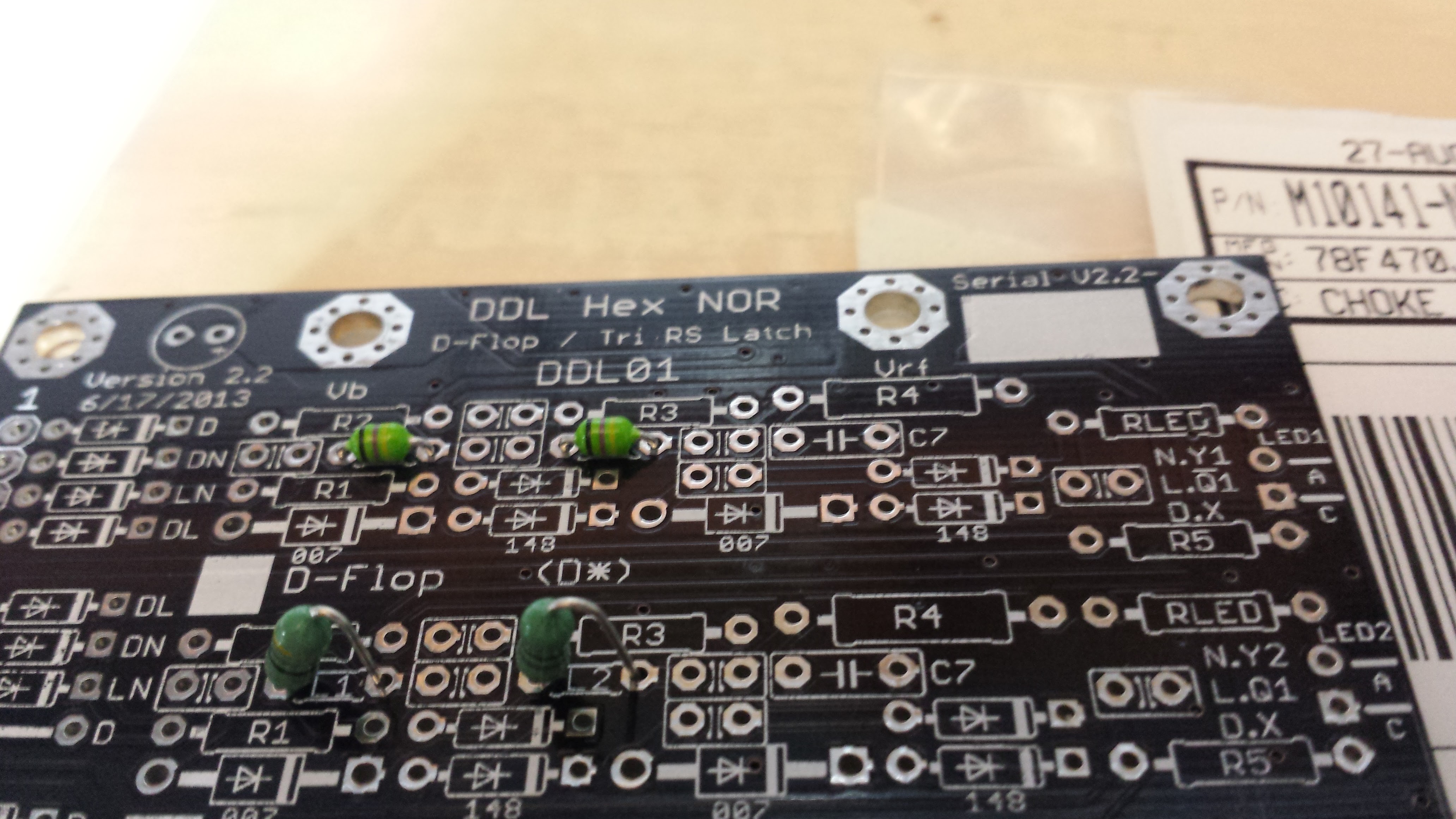
The DDL01 board can be configured at build-time as six NOR gates, three RS latches, or a single (negative) edge-triggered D flip-flop. Here's how. Next to each jumper or diode on the input row, there are one or more letters or "*". They mean this:
- D : populate for D-flop
- N : populate for NOR
- L : populate for Latch
- * : always populate
The silkscreen makes clear if there's a diode or jumper expected in each position. You can see these letters on the left hand of the board photo above, next to the input diode and jumper sites.DDL01: R4
R4 on the DDL01 is a 1/2W unit - it dissipates more than you want on a 1/4W unit (less than 250 to maintain a 2x de-rating, though). All other resistors are 1/4W. R4 is 220 Ohms for normal gates (with front-panel LEDs) but I switched to 150 Ohms for boards driving the seven-segment displays to get better brightness. Since there are six displays, there are 6*7 = 42 segments, and you need 42/6 = 7 boards populated this way. The diodes on the DDL03 encoder ROM are also used as the input diodes for the segment driver boards - see below. I'll document this in more detail when I describe the display boards in a separate log entry.
Also note that there are six resistors designated "R4" on the board. In fact, all of the corresponding gate components are designated identically: "R4" means the same thing to each gate. Unconventional, perhaps, but I found it useful.
Segment Driver Boards
Seven DDL01 boards are specially configured as segment drivers for the clock display. As mentioned above, these boards are fitted with 150 Ohm 1/2W resistors at the six "R4" sites to boost display brightness. In addition, the performance is improved by eliminating the redundant input diodes on this board. Since the DDL03 encoder ROMs are already a diode input matrix for the display drivers, input diodes on the seven segment-driver boards are unnecessary and simply hurt performance. So, to improve things a bit, no input diodes are used on the segment driver boards. The "NOR" gate diode positions (indicated with an "N" next to the input diode sites on the DDL01) are simply populated with wire jumpers. This only applies to the seven boards used as segment drivers.
DDL01 Datasheet
You should probably approach anything in the datasheet with caution. The PIN-diode properties of the 1N4007 are not guaranteed by *its* datasheet (it's just a rectifier diode, after all), so depending on the manufacturer and lot, you might get better or worse (or no) performance in this application. I have never seen a 1N4007 (or 1N400x for that matter) that didn't work at some level, but you might run into them. For a good time, google "1N4007 PIN diode" and read what some of the hams have to say on the issue. I used Fairchild 1N4007 diodes in all my DDL circuits, although I have sampled other manufacturers. I suspect that some of the 1N400x series you may encounter are actually 1N4007s sold as lower-spec parts (like selling 1% resistors as 5%), but don't count on it.
Power Consumption
The whole clock consumes 60W (measured at the 12V DC supply input), regardless of the clock speed (it's not CMOS!). Roughly, this means that each board consumes 60/46 = 1.3W, and each gate 1.3/6 = 220mW.
RF Emissions
You are responsible for complying with any laws or rules concerning electromagnetic interference in your country or jurisdiction. Each DDL02 power supply can deliver 35W of RF power in the high-frequency band. Four such boards are used in the clock, enough to easily cause serious interference to other devices, including amateur radio, government, or emergency radio services in the HF band. An "open" case style can exacerbate the problem.
The clock uses a spread-spectrum approach (documentation forthcoming) to try to mitigate any emissions problems, but it has not been thoroughly tested as of now. By building or operating this device you may cause harmful interference and/or subject yourself to legal penalty. I don't run my clock for extended periods at the moment, and won't until I am sure it isn't emitting harmful interference.
-
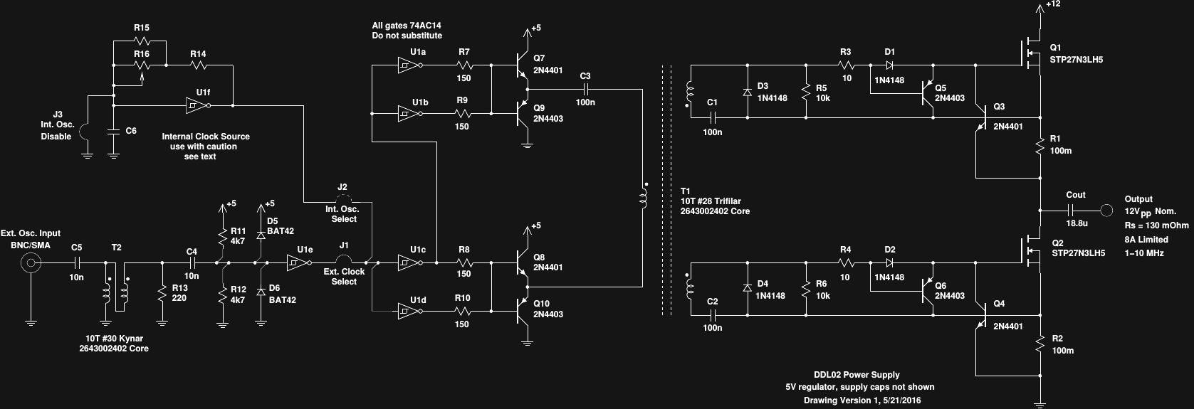
DDL02 Power Supply [Part 1]
05/18/2016 at 16:01 • 0 commentsI decided to split the DDL02 documentation into multiple parts because I want to get something out there, but have to fix up some of the material before I post it all. When I developed the board, I wasn't very good about consistent part designations between the simulation, the "publication" schematic, and the board design files. It might confuse somebody (everybody?), so I'm fixing it all first. The board layout, of course doesn't need to change.
I used aluminum organic polymer caps on the DDL02 for their very low ESR, high allowed ripple current, good high-frequency response, and long life. Unfortunately, the original parts I used are now a factory special-order, so I'm in the process of finding suitable replacements. The good news is that there are now a wider variety of parts available (cheaper, too), but these are specialized caps, and it's not just a matter of finding one that physically fits on the board. A full BOM and assembly guide will be forthcoming shortly, but not in this post. Assembly of the power supply board is significantly more complex than the logic boards (which are essentially bulletproof), and it's important to get right (or risk popping MOSFETs).
Power Supply Requirements
The DDL02 power supply is designed to be mounted on the left side of a DDL logic stack. Here, you can see three of the four stacks used in the clock, each with their respective power supply board mounted on "top" (these stacks are rotated 90 degrees CCW before mounting).
![]()
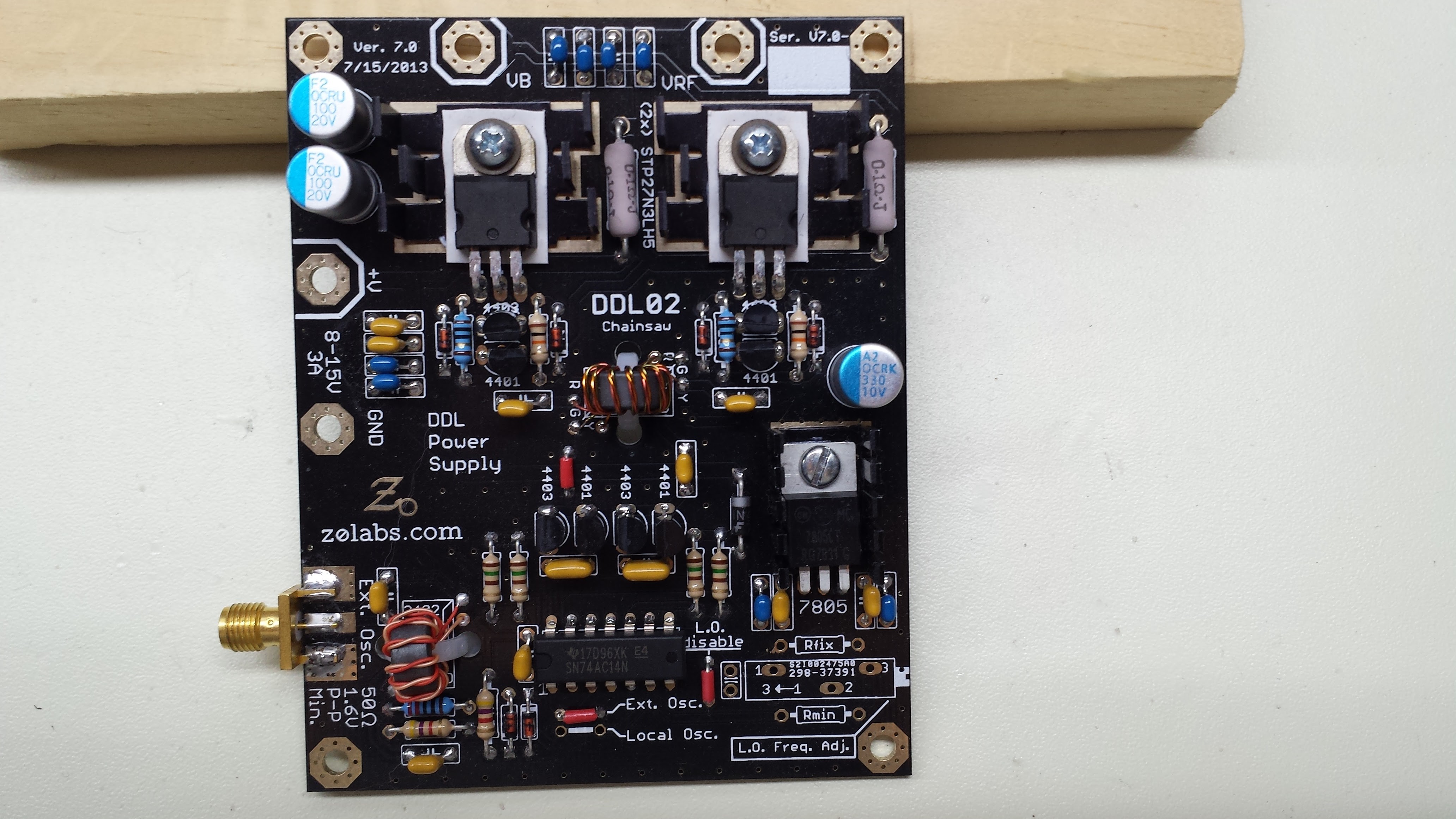
Here's one of the board itself:
![]()
DDL requires a fairly specialized power supply, with 5V DC bias and low-impedance RF available. The 5V supply is similar to countless others - a simple 7805 drops the 12V down to 5, and a liberal sprinkling of bypass caps keeps noise at bay.
The RF supply is a different matter entirely. The DDL01 NOR board functions well with an RF supply of between 10-12 V peak-peak, and the power supply is expected to deliver that to between 1 and 20 boards per "stack". Most RF systems you'll encounter use impedance matching, in which the load impedance is matched to the source and/or transmission line impedance (typically 50 or 75 ohms). This is done to maximize power transfer as well as prevent reflections and standing waves on structures a significant fraction of a wavelength in size. Unfortunately, implementing impedance matching in a DDL system designed for modularity isn't very practical. Instead, impedance "bridging" is used, in which the source impedance is low compared to the load (similar to audio amplifiers). The DDL02 presents a source impedance of around 130 milliohms, while the expected maximum loading (20 DDL01 boards) is around 1.1 ohm. This is all at frequencies between about 1 and 10 MHz. It's not your usual HF amplifier.
History
Just for fun, this is the "Evolution of Man" chart for the DDL power supply. Except here, they're all monkeys :-)
![]()
The last one on the right is essentially the same as the final PCB, and even has the correct holes and contacts for mounting on a DDL stack:
![]()
I started with complementary bipolar output devices (it's a half-bridge output driver on all but the first board), moved to complementary MOSFETs, then finally settled on two high-performance N-channel devices. Before this project, I was a little hesitant to design MOSFETs into my circuits - who needs a part that you can destroy at a touch (or, through the magic of induced charge, at the wave of a hand)? Contrast this with the humble diode, used universally as an ESD protection device. I got over it.
Design
My go-to resource for designing the supply was "Design and Application Guide for High Speed MOSFET Gate Drive Circuits" by Laszlo Balogh. You can download it here - this an external link, so if it disappears, just search for the title. I can't recommend this paper enough - if you're designing a high-speed driver with discrete components, read this paper first. Beginning to end. It will save you a lot of time.
Before I designed this circuit, I looked for suitable integrated MOSFET half-bridges and/or drivers, but could find none that offered the combination of speed and power required. However, I wouldn't be surprised if such a thing exists. If you find one, let me know.
The schematic looks like this. Click here for a nicer pdf version.
![]()
Starting with the output devices, you can see that the the high and low-side drivers are identical, and driven out of phase by two opposing transformer windings. If you build one, take careful note of the transformer phasing dots. Ignoring current-limiting for the moment, the output devices are theoretically capable of shorting over 90 Amps through each other if both turned on at the same time. Just don't do it.
The output devices used on the boards are STP27N3LH5 power MOSFETs from ST Microelectronics. A close substitute would be the PSMN022-30PL by NXP Semiconductors. I actually developed the LTspice simulation using the NXP part, because the SPICE model is readily available (see below for simulation details), but used the improved-spec ST part on the boards.
Since the high- and low-side driver circuits are identical, we'll concentrate on Q1 first. R1 and Q3 form a simple current limiter. Note the lower-case "m" - R1 is 100 milliohm, or 0.1 ohm, not 100 megaohm. When more than around 0.7V is dropped across R1, Q3 cuts off the gate drive to Q1, limiting the output current. In practice, and at the operating frequency, this limits current to about 8A peak. The result is a simple but fairly crude limiting. During limiting, the "extra" voltage, and hence power, is dropped across Q1, causing excessive dissipation. This circuit is intended to protect against momentary shorts (like accidentally grounding the output with the tip of a screwdriver), not prolonged overloads. Running this circuit in current-limiting will fry the MOSFETs eventually. The output also rings pretty badly when in limiting. Again, try not to do this.
Q5 and D1 form a "local" turn-off circuit, turning off Q1 much faster than waiting for the gate to discharge back through the transformer. To maximize the effectiveness, these parts are as close as possible to the MOSFET, keeping the gate discharge current loop small. Balogh provides a good description of this technique. While Q5 speeds the turn-off, R3 is intentionally chosen to work with the gate capacitance to slow down the turn-on. Since the high and low-side drivers are continuously alternating drive, it's important to keep them from overlapping their on-time. Even a brief overlap would mean considerable shoot-through, decreasing efficiency and increasing noise at the very least. With the design value (R3=10 ohms), I could not detect any shoot-through spikes when testing current through MOSFETs with an improvised ferrite-ring current probe. The simulation waveforms are similarly clean.
R5 serves as a power-up protection device, keeping the gate voltage low at turn-on. C1 and D3 serve to restore the DC level on the transformer secondary, clamping the negative excursions to one diode drop below Q3's source and ensuring an adequate positive gate drive voltage. Again, Balogh provides good insight.
Transformer T1 provides 180-degree phased drive to the high-side and low-side drivers. The transformer is easily wound, with some caveats. My transformers were wound on my favorite HF core, the Fair-Rite 2643002402. Mouser sells them for $0.061 (qty 100), and it works very well for broadband transformer applications like this one. The windings were done with 28-gague magnet wire, twisted together with a hand drill, then wound 10 turns on the core. I used three different colors of wire to keep the windings straight. Mixing up phasing on one of the secondaries would cause both output MOSFETs to turn on simultaneously, with disastrous results.
I will be evaluating some alternative cores on the board to verify that they work properly, and determine if they require different winding.
On the primary side of the transformer, C3 blocks DC to keep excessive current from flowing when the board is not driven (e.g. at startup or during bench testing), and eliminate any chance of DC magnetizing current from asymmetrical drive waveforms. The transistors Q7-Q10 form an H-bridge with emitter followers to dive the transformer primary in push-pull, doubling the available amplitude from the 5V supply. The transistors, in turn, are driven from paralleled 74AC14 gates (U1a-U1d). The AC-series logic drives enough current for this task; HC or TTL would not.
The clock to drive the 74AC14 push-pull stage is jumper-selected from an on-board RC relaxation oscillator or an external input. I have never used the on-board oscillator option. It was intended for small stand-alone DDL systems where the expense or complexity of the spread spectrum source was prohibitive. I also hesitate to use this source because, as a narrow-bandwidth (albeit not particularly stable) signal, it has more potential to cause interference than the spread-spectrum source. Should you decide to use it, use either R14 and R16 for a variable frequency oscillator, or just R15 (and shunt R14 with 0 ohms).
The DDL04 spread spectrum source is connected to the board through an end-launch SMA or BNC connector (builder's choice, the board will fit either). For testing purposes, a normal signal generator can be connected as well. TTL-level signals will work, as well as general 50-ohm signal generators of at least +7dBm output. The input has a reasonably good match to 50-ohms. T1 matches this to 200 ohms on the secondary, which is terminated by R11-R13. I wound this transformer with a bifilar pair made from 30 gauge wire-wrap wire because the pair has approximately 100 ohms impedance, ideal for matching 50 to 200 in a broadband transformer. In practice, a 28ga bifilar magnet wire winding (closer to 50 ohms impedance) would probably work just as well here. R11 and R12 bias U1e at mid-supply, while D5 and D6 provide protection against ESD at the input. On prototype versions of the board, I used 1N4148s here, but finally decided on the Schottkys for the production boards.
Simulation
I've uploaded an LTspice simulation for the power supply here. Since I don't have a SPICE model for the STP27N3LH5 MOSFET, I used a very similar part, the NXP PSMN022-30PL for simulations. The two parts are very similar, and probably interchangeable in this design, but I haven't tested the NXP device on actual boards. Unfortunately, even though a SPICE model is available, I can't make heads or tails of the licensing, so if you want to use it, you can download it yourself from NXP here: PSMN022-30PL SPICE model. The simulation as I supply it uses the Fairchild FDS6630A, a popular part with similar gate parameters that simulates fairly close to the others, but comes in the wrong package for this design, has a higher Rds, and handles less current. On the plus side, a model for it comes with LTspice. I found the spice simulations invaluable in doing this design. I'm sure it saved me a small pile of cash in burned MOSFETs (didn't lose a single one).
Next
Once I have sorted out the part designations, replacement caps, and BOM, I will post the board designs so interested parties can have some fabbed, or modify the design as required.
-
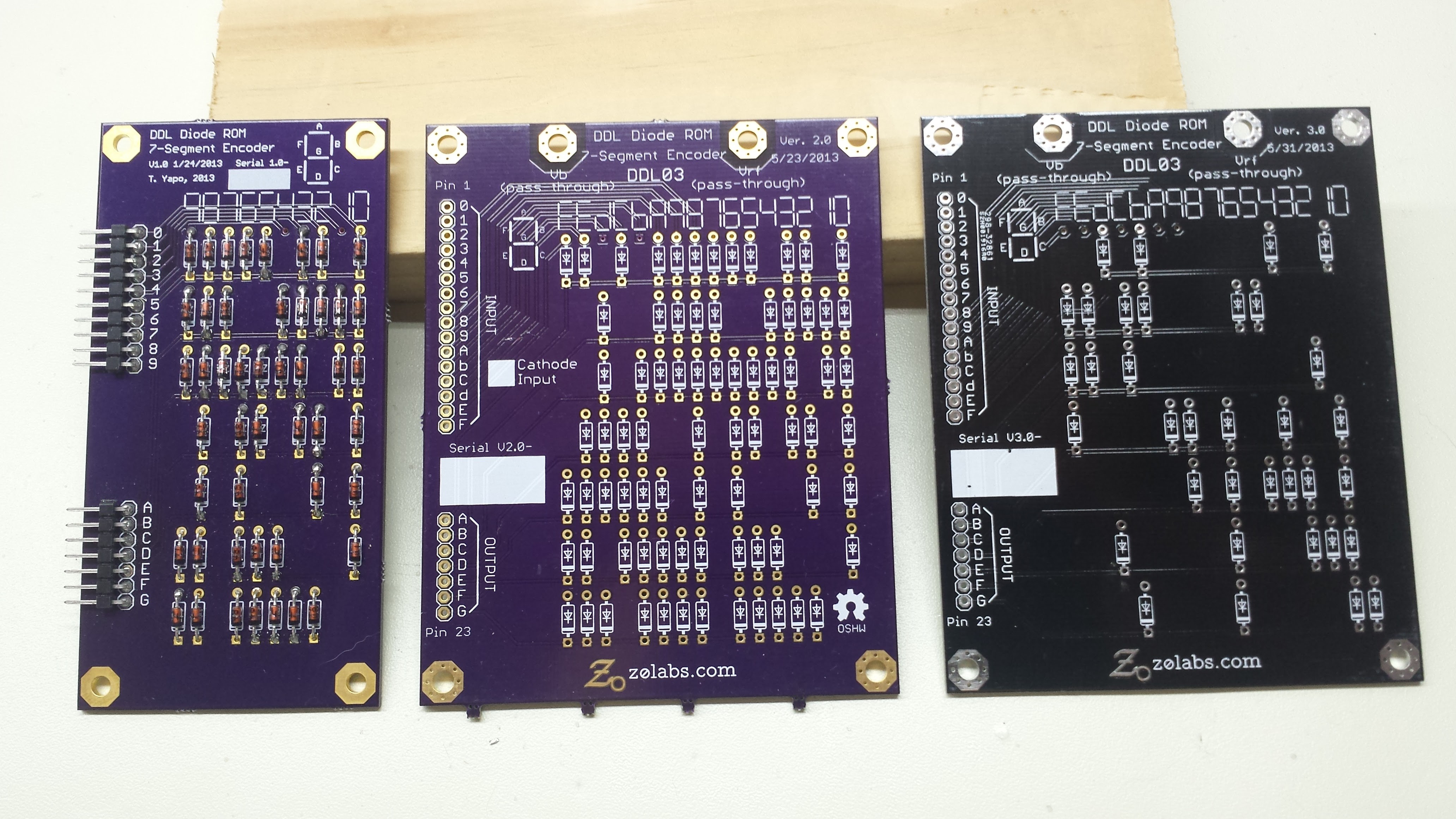
DDL03 7-Segment Encoding ROM
05/16/2016 at 20:53 • 4 commentsThe design for the 7-segment encoders is trivial: they're just diode ROMs. So, of course, it took me three spins of the board to get it right!
![]()
On the far left is the DDL 1.x encoder board, designed for numerals 0-9 only. In that design, the segment drivers were to be non-inverting, so a diode was required in the matrix for every lit segment. In the middle was the first spin of the encoder for DDL 2.x. Since I had extra room on the new DDL board size, I added AbCdEF to the matrix, so hexadecimal could be displayed. It's not used on the clock, but it would be perfect for the display on a simple computer. While those boards were being fabbed, I re-designed the segment drivers to use inverting logic - now a diode is required for each segment that is off. Another spin. Conveniently, the final version uses far fewer diodes. I had never realized the disparity between the number of on and off segments on a display before. There's probably something deep about the information efficiency of 7-segment displays in there somewhere. But I can't find it.
If you need a place to park 34 diodes, you can:
Next up: the power supply. Fast, powerful MOSFETs.
The Diode Clock
A digital clock built with Diode-Diode Logic (DDL), a quirky new logic family using only common diodes and passive components.

 1 kHz
1 kHz
 2 kHz
2 kHz
 3 kHz
3 kHz
 4 kHz
4 kHz
 5 kHz
5 kHz
 1 kHz
1 kHz
 2 kHz
2 kHz
 3 kHz
3 kHz
 4 kHz
4 kHz
 5 kHz
5 kHz
 1 kHz
1 kHz
 2 kHz
2 kHz
 3 kHz
3 kHz
 3.3 kHz
 3.6 kHz