 E. N. Hering
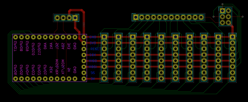
This is the first version of the system backbone. The MCU modules will be plugged to this PCB. The MCU module footprint present on the board is there to receive the communications module, which calls each of the plugged modules, sending or receiving data depending on the module function. In this board is also present a ISP connector to program each module separately and a 12 pin header that will connect the ISP reset to the RESET of the module that will be programmed. Finally, a 4 pin connector is also present, connecting the COM module with the wifi transceiver, via a serial connection. All this information in only one paragraph sounds confusing, I know. If you have questions, please ask. As always, comments are welcome.
Discussions
Become a Hackaday.io Member
Create an account to leave a comment. Already have an account? Log In.