SHAOS
SHAOS-
efabless is gone :(
3 days ago • 0 commentsefabless has shut down operations, so no more chips through them :(
![]()
but TinyTapout is still around and they say they will look for other ways to make chips: https://www.linkedin.com/posts/tinytapeout_were-very-sad-to-hear-that-efabless-corporation-activity-7301638170297720832-n7Ru/
-
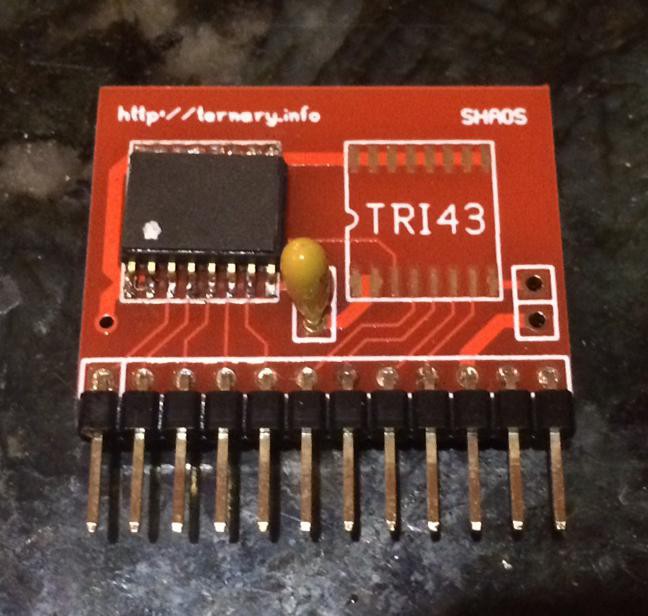
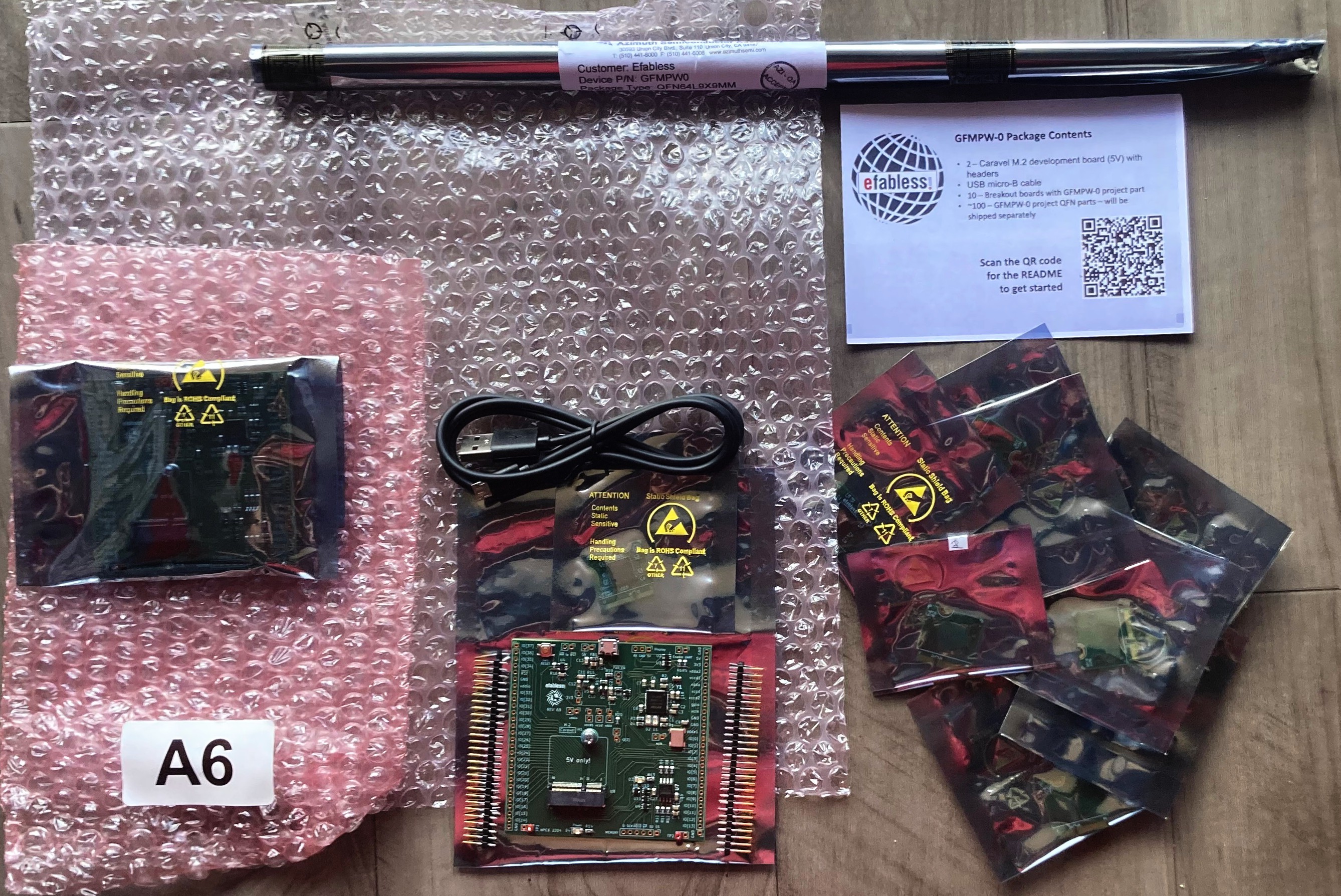
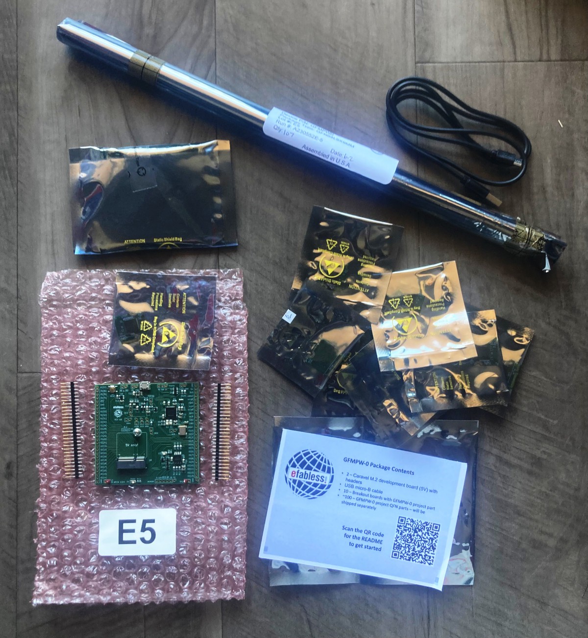
Received my chips from efabless
07/27/2023 at 07:22 • 0 commentsReceived 2 packages from efabless - both my designs were manufactured:
![]()
![]()
Each package has USB-cable, 2 motherboards, 10 daugher-boards with chips and 100+ chips packahed in QFN64.
Process of testing of those chips is described in different Hackaday-project:
https://hackaday.io/project/192099-lab-computer-marina
And another way - TinyTapeout - is not yet ready....
-
Trying other ways to make chips
12/05/2022 at 03:27 • 8 commentsCurrently I'm trying to jump to the last car of efabless train :)
- made a few test designs for TinyTapout that goes with efabless 130nm process as part of TT02;
- and also submitted 2 open source test designs to efabless 1st 180nm process that should go through GlobalFoundries
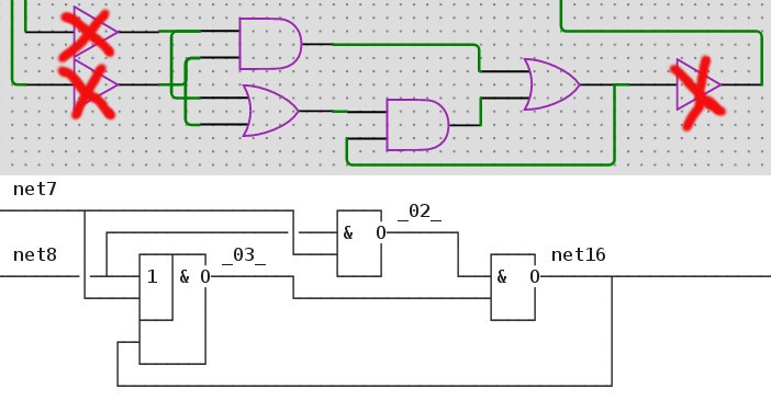
Nothing fancy, because everything is done through Verilog - you can actually draw your schematics in Wokwi but it's eventually converted to Verilog as well. Good thing is that self-made latches are translated to low level almost as is:
![]()
This is a Muller gate (or C-gate) and if it will work as intended on actual chip then it means async designs are very possible with this Yosys driven process :)
-
Estimation of area for ternary selector
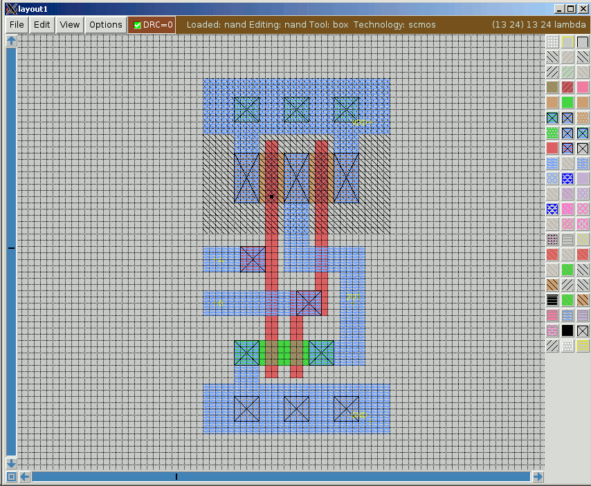
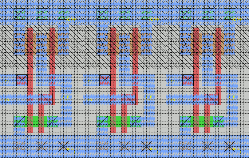
12/17/2017 at 03:05 • 0 commentsIn order to calculate how heavy TRIASIC could be with current limitations let's estimate how compact a ternary selector could be using our library of gates. If you paid attention to this project then you probably remember that ternary selector (multiplexer/demultiplexer) on 1st chip was implemented from binary gates manifesting analog behavior as showed below:
![]()
This is how it looked in "spread" form (large squares are "filler cells" that do nothing):
![]() So one ternary selector has:
So one ternary selector has:
3-input NAND gates: 2
3-input NOR gates: 2
2-input NOR gates: 1
NOT gates: 6
Transmission gates: 3
TG and NOT gates are "low-profile" gates that could be only 53 units high and 3-input gates have 64-unit height. We can arrange elements in 2 rows - NOT and TG in one row and NAND/NOR in another row.
Width of elements:
3-input NAND gate - 38 units
3-input NOR gate - 38 units
2-input NOR gate - 30 units
NOT gate - 22 units
Transmission gate - 29 units
1st row (NOT and TG): 6*22+3*29=219 units wide and 53 units high
2nd row (NAND and NOR): 4*38+30=182 units wide and 64 units high
Between rows we will have 7+7+3=18 units for 2 metal interconnects, so total height will be 53+64+18=135 units (47um) and total width 219 units (77um) - this is 20 modules from side to side horizontally and vertically we can put 25 rows of such modules (if we allocate space between them for 5 metal lines of interconnects) or totally 20*25=500 ternary selectors.
And at the end one more picture from that 1st chip ;)![]()
-
NAND ASIC
12/10/2017 at 08:27 • 0 commentsI have an idea of "NAND ASIC" in 2x2 mm when on chip itself we only have 2-input NAND gates and metal layers do interconnects between those NAND gates to implement something as NEDONAND in silicon :)
Let's count how many gates we may have - 1 gate occupies 30x57 units (lambdas) that is 10.5x20 um:
![]()
We have 2000x2000 um area where we will put pads and power rings so available area will be about 1550x1550 um. NAND gates may be arranged in the rows one after another like this:
![]()
So in 1 row we may put 147 2-input NAND gates. Then we may have a number of horizontal lines in metal layer 1 or 2 after each row for interconnect - every line will take 3 lambdas for spacing and 4 lambdas for metal itself, so it's 7 lambdas per line plus additional 3 lambdas per spacing between next row of NAND gates. Let's calculates how many gates we may put on single chip if we will have N metal lines between rows of NAND gates:
N=3 : interconnect will take 3*7+3=24 lambdas or 8.4um so height of every row will be 28.4um and on the chip we may have 1550/28.4=54 rows or 147*54=7938 NAND gates
N=5: 5*7+3=38 lamdas or 13.3 um so 33.3 um for row, 1550/33.3=46 rows or 147*46=6762 NAND gates
N=7: 7*7+3=52 lamdas or 18.2 um, 38.2 um for row, 40 rows or 147*40=5880 NAND gates
N=9: 9*7+3=66 or 23.1 um, 43.1 um for row, 36 rows or 5292 NAND gates
I'm still not sure how many interconnection lines will be good enough for most designs - probably I need to "synthesize" something 1st to see how it will go...
P.S. Next step - to design compact layout for ternary multiplexer/demultiplexer ( see https://hackaday.io/project/11779/log/47306-useful-outcome ) to make ternary ASIC prototype as well (half of the chip might be binary NAND-ASIC prototype with for example NEDONAND implemented and another half - ternary TRI-ASIC prototype with for example parts of TRIADOR implemented ; )
-
Planning next "tapeout"
12/02/2017 at 04:03 • 10 commentsAccording to this page:
https://www.mosis.com/db/pubf/fsched?ORG=ON-SEMI
in 2018 MOSIS will collect C5F/C5N 0.5um designs on these dates:- April 2nd
- August 6th
- December 3rd
So we can choose April 2nd, 2018 as possible next "tapeout" date for our 2nd chip - anybody interested? ;)
Maximal possible size of the die for minimal cost is 4 mm^2 now (it could be square 2x2 mm or 2000x2000 um) and we will order minimal possible quantity - 40. Planned packaging was DIP40, so die may have 40 pads on it (10 pads on each side of the die). Our old pad generator will not work, because last time die had slightly bigger size - 2.2x2.2mm (to meet 5mm^2 limit at that time).
Technically possible to put more pads - if we will keep the same sizes and spacing as last time (100x100um pads with 50um between each other and 25um from pads to border - actually it was recommended size by MOSIS) then we can put N*150 on each side and for 2000um it will be N=13, so it's 13+13+11+11=48 max and now, surprise-surprise, DIP48 is also available as an option for packaging (even though slightly more expensive)!
Now I plan to have everything OPEN SOURCE and fully available on every stage of the work under PUBLIC DOMAIN :)
-
Useful outcome
10/09/2016 at 15:49 • 0 commentsAs I said before my 1st chip is a collection of test circuits for binary, ternary and quaternary building blocks. One of that building blocks could be used directly even right now - it is ternary selector (that could connect 1 pin to any other 3 using 1-wire ternary control). SOIC16 package has only this building block wired to pins with this pinouts:
Pin 1 - Vss (negative voltage)
Pin 2 - MUST BE GROUNDED (Vss)
Pin 3 - S (analog input "select")
Pin 4 - N (analog input/output "negative")
Pin 5 - O (analog input/output "neutral")
Pin 6 - P (analog input/output "positive")
Pin 7 - C (analog output/input "common")
Pin 8 - Vdd (positive voltage)
Pin 9 - MUST BE GROUNDED (Vss)
Pin 10 - NOT CONNECTED
Pin 11 - NOT CONNECTED
Pin 12 - NOT CONNECTED
Pin 13 - NOT CONNECTED
Pin 14 - NOT CONNECTED
Pin 15 - NOT CONNECTED
Pin 16 - Vss (negative voltage)
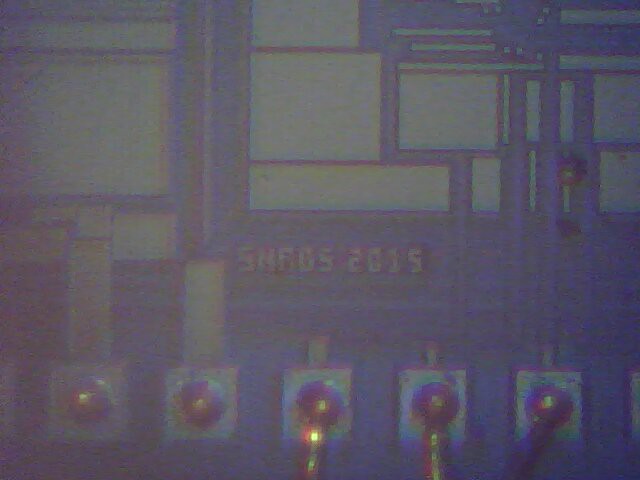
I designed a break-out board to convert SOIC to SIP (breadboard friendly):
It's working pretty well (except the fact that switching frequency is limited to 20 kHz):![]()
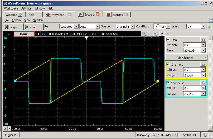
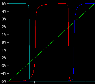
Oscillograms if selector connected as ternary buffer (N = -5V, O = 0V, P = +5V):![]()
Oscillograms if selector connected as ternary inverter (N = +5V, O = 0V, P = -5V):![]()
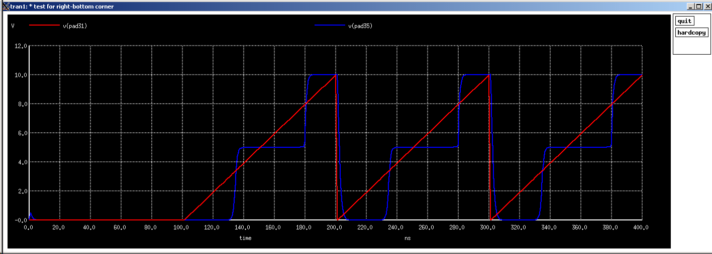
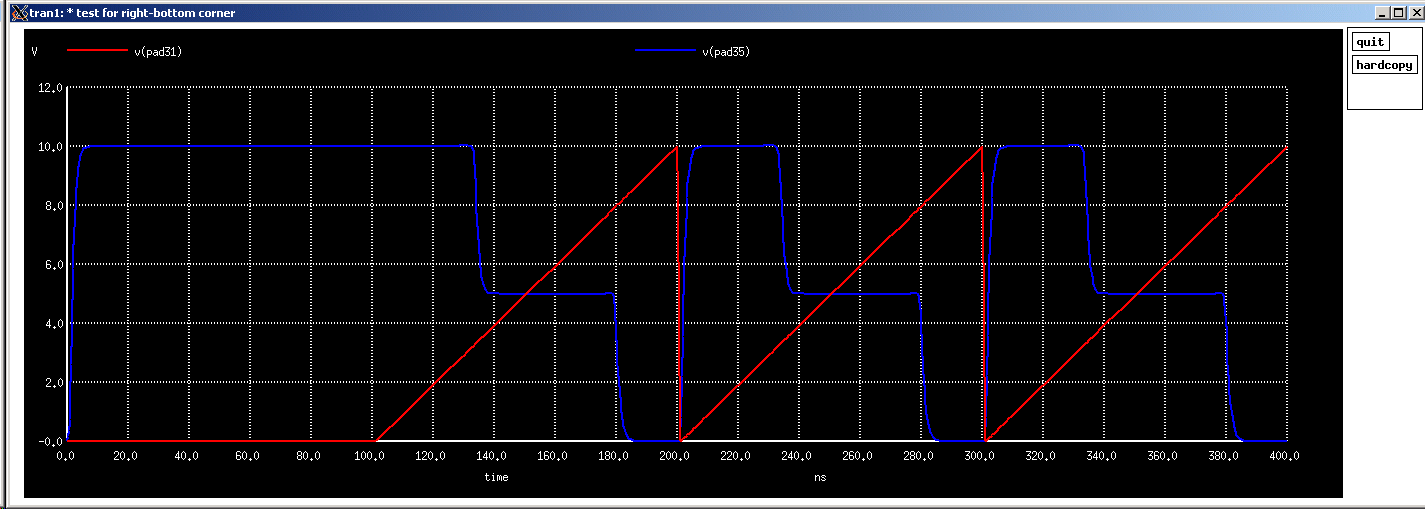
And below you can see respective SPICE simulations generated by ngspce on model extracted from final chip layout (with models of PMOS and NMOS transistors for chosen CMOS technology found on Internet):![]()
![]()
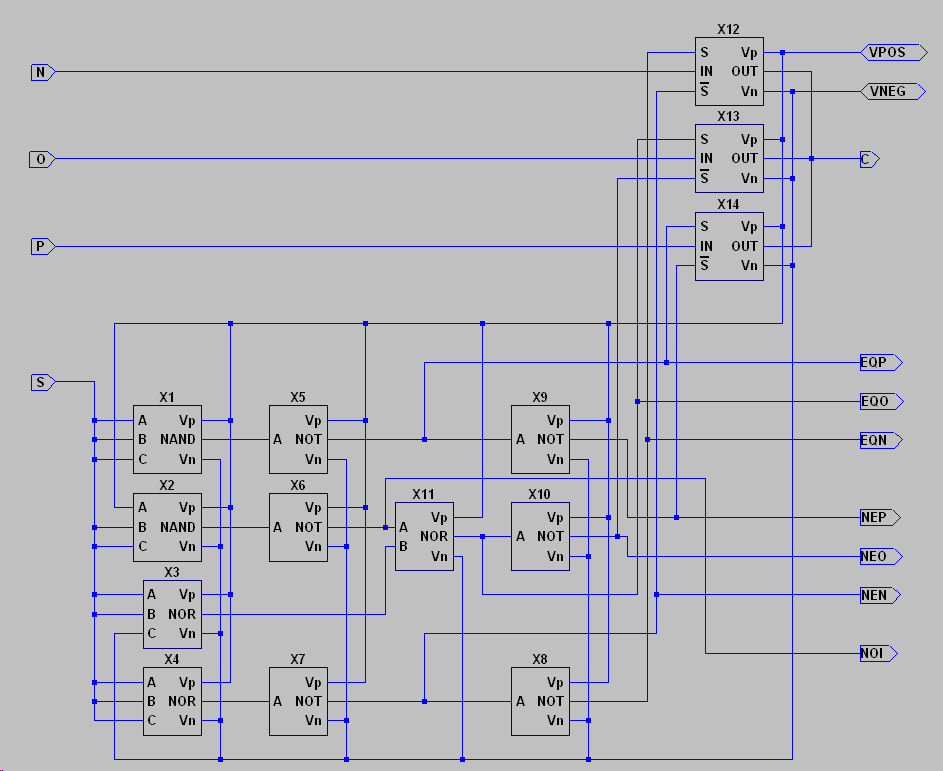
Schematics of this selector:![]()
Above ternary circuit is based on regular binary blocks described before - NOT, NAND, NOR and TG. Here I use effect of shifting of threshold of NAND and NOR binary gates if all or some inputs connected together (LTspiceIV simulation):![]()
![]()
![]()
As you can see there are gaps between active zones (kind of "break-before-make" non-shorting transition) to prevent switches (X12,X13,X14) to be ON simultaneously while moving between zones (and it may cause short circuits between power lines because any of pins N,O,P could be connected to most positive or most negative voltage to implement some ternary functions using this universal ternary selector).
-
Filling cell
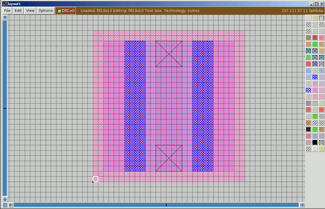
10/07/2016 at 04:00 • 0 commentsManufacturing required to fill all empty spaces by some filling cells that have metal layers and poly to meet density rule - this should support all neighboring designs. I created this cell 10x10um with 3 metal layers and poly layer connected to each other:
![]()
This is how CIF-viewer showed this (and how it looks on actual silicon - with "fingers"):
![]()
Problem is (and I think it's main reason of chips slowness) there is no connection to the ground (P-substrate here)! So chip is having a lot of floating capacitors between signals and ground that eat all dynamic - it has to be fixed before 2nd tapeout...
-
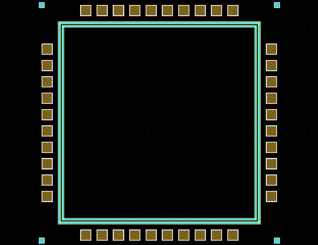
Pads generator
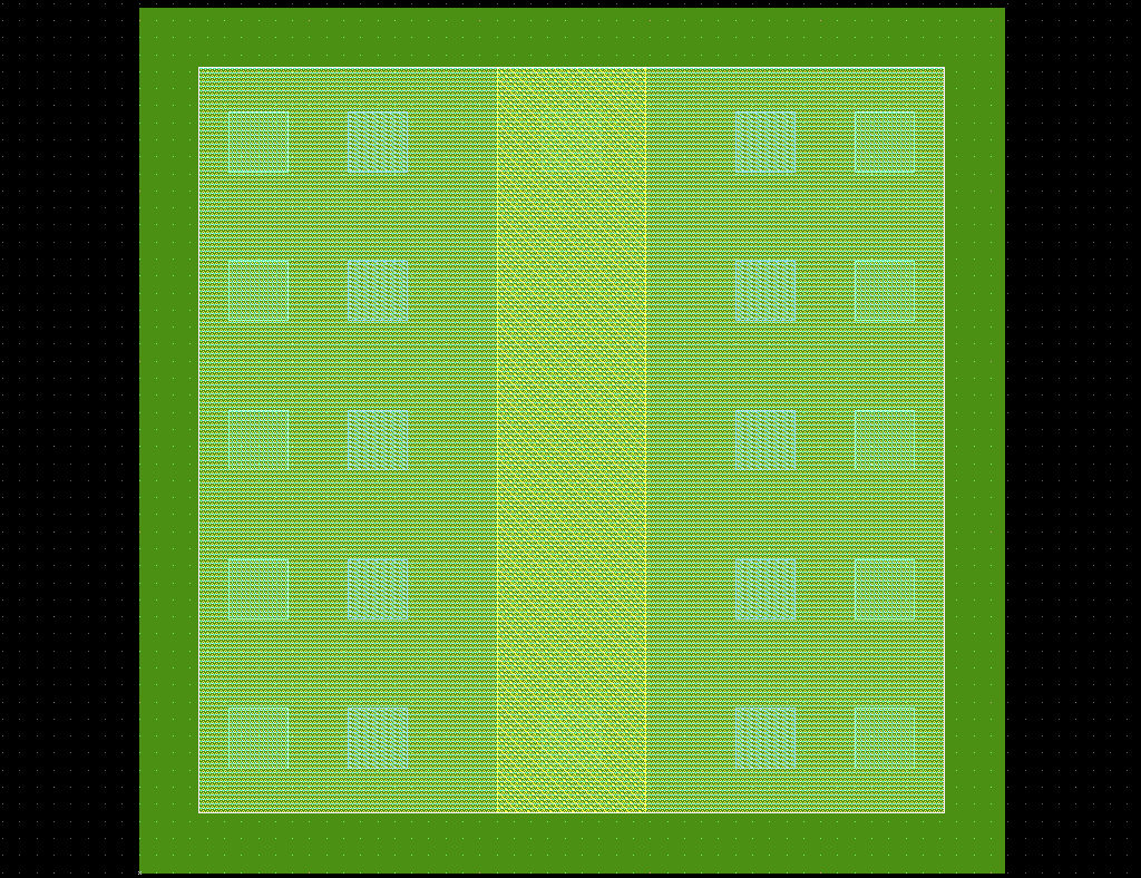
10/04/2016 at 19:49 • 10 commentsThis simple straightforward script generates 40 pads (each 100x100um) and power rings (VDD & VSS) for 2.2x2.2mm CMOS 0.5um design (silicon proven in 2015):
# Generating DIP40 pads and VDD/VSS rings for SCN3M 0.5um process
# This script is PUBLIC DOMAIN - use it on your own risk!
rm -f pad.* pads.*
magic  -T SCN3M.35 -dnull -noconsole << EOF
drc off
box position 0 0
box size 100um 100um
paint pad
label IO
save pad
cif
erase
cellname rename pad pads
# Pads
box position 2085um  980um
getcell pad
box position 2085um 1130um
getcell pad
box position 2085um 1280um
getcell pad
box position 2085um 1430um
getcell pad
box position 2085um 1580um
getcell pad
box position 2085um 1730um
getcell pad
box position 1730um 2085um
getcell pad
box position 1580um 2085um
getcell pad
box position 1430um 2085um
getcell pad
box position 1280um 2085um
getcell pad
box position 1130um 2085um
getcell pad
box position  980um 2085um
getcell pad
box position  830um 2085um
getcell pad
box position  680um 2085um
getcell pad
box position  530um 2085um
getcell pad
box position  380um 2085um
getcell pad
box position   25um 1730um
getcell pad
box position   25um 1580um
getcell pad
box position   25um 1430um
getcell pad
box position   25um 1280um
getcell pad
box position   25um 1130um
getcell pad
box position   25um  980um
getcell pad
box position   25um  830um
getcell pad
box position   25um  680um
getcell pad
box position   25um  530um
getcell pad
box position   25um  380um
getcell pad
box position  380um   25um
getcell pad
box position  530um   25um
getcell pad
box position  680um   25um
getcell pad
box position  830um   25um
getcell pad
box position  980um   25um
getcell pad
box position 1130um   25um
getcell pad
box position 1280um   25um
getcell pad
box position 1430um   25um
getcell pad
box position 1580um   25um
getcell pad
box position 1730um   25um
getcell pad
box position 2085um  380um
getcell pad
box position 2085um  530um
getcell pad
box position 2085um  680um
getcell pad
box position 2085um  830um
getcell pad
# Corner markers
box size 50um 50um
box position 0 0
paint psc
box position 2160um 0
paint psc
box position 2160um 2160um
paint psc
box position 0 2160um
paint psc
# Ground ring
box position 175um 175um
box size 1860um 1860um
paint m1
box position 180um 180um
box size 1850um 1850um
paint psc
box position 195um 195um
box size 1820um 1820um
erase
paint m1
box position 178um 178um
box size 20um 20um
erase
paint m1
box position 180um 180um
box size 15um 15um
paint psc
box position 2012um 2012um
box size 20um 20um
erase
paint m1
box position 2015um 2015um
box size 15um 15um
paint psc
paint m1
box position 178um 2012um
box size 20um 20um
erase
paint m1
box position 180um 2015um
box size 15um 15um
paint psc
paint m1
box position 2012um 178um
box size 20um 20um
erase
paint m1
box position 2015um 180um
box size 15um 15um
paint psc
box position 200um 200um
box size 1810um 1810um
erase
# Power ring
box position 210um 210um
box size 1790um 1790um
paint nw
paint m1
box position 215um 215um
box size 1780um 1780um
paint nsc
box position 225um 225um
box size 1760um 1760um
erase
paint nw
paint m1
box position 213um 213um
box size 15um 15um
erase
paint nw
paint m1
box position 215um 215um
box size 10um 10um
paint nsc
box position 1982um 1982um
box size 15um 15um
erase
paint nw
paint m1
box position 1985um 1985um
box size 10um 10um
paint nsc
box position 213um 1982um
box size 15um 15um
erase
paint nw
paint m1
box position 215um 1985um
box size 10um 10um
paint nsc
box position 1982um 213um
box size 15um 15um
erase
paint nw
paint m1
box position 1985um 215um
box size 10um 10um
paint nsc
box position 230um 230um
box size 1750um 1750um
erase
save pads
cif
quit -noprompt
EOF
Result is pads.mag file (and pads.cif just in case) that looks like this:
![]()
-
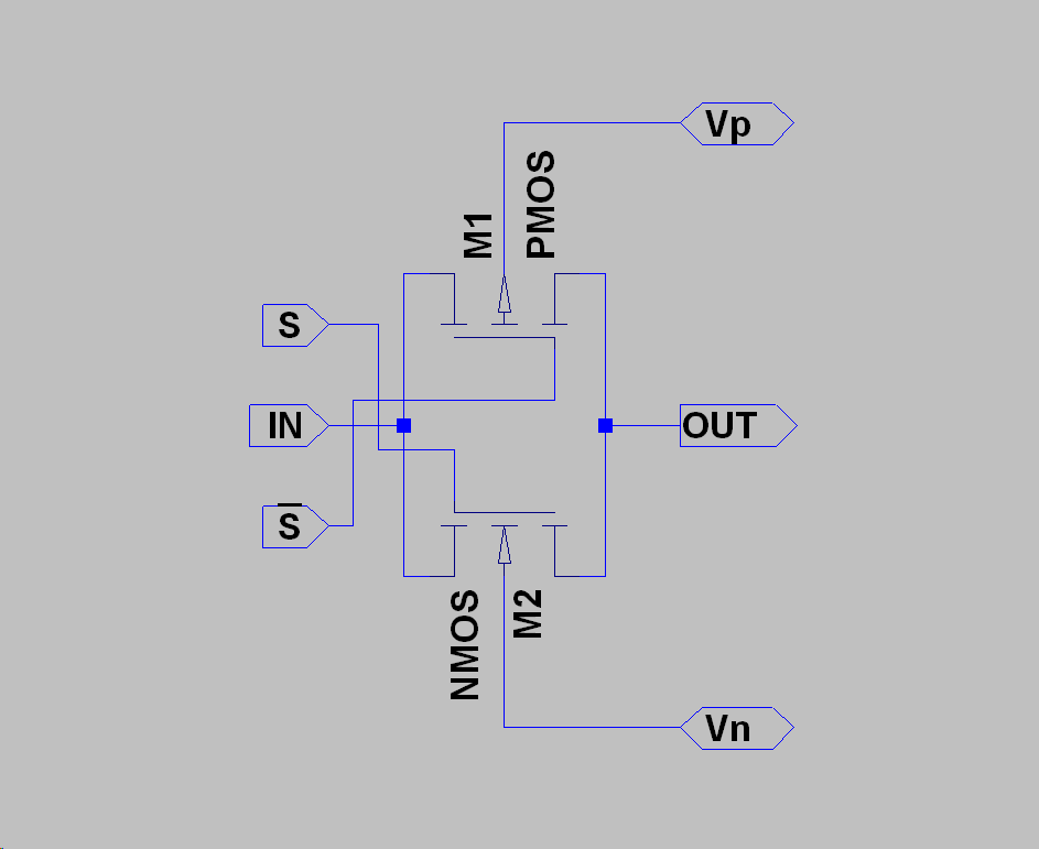
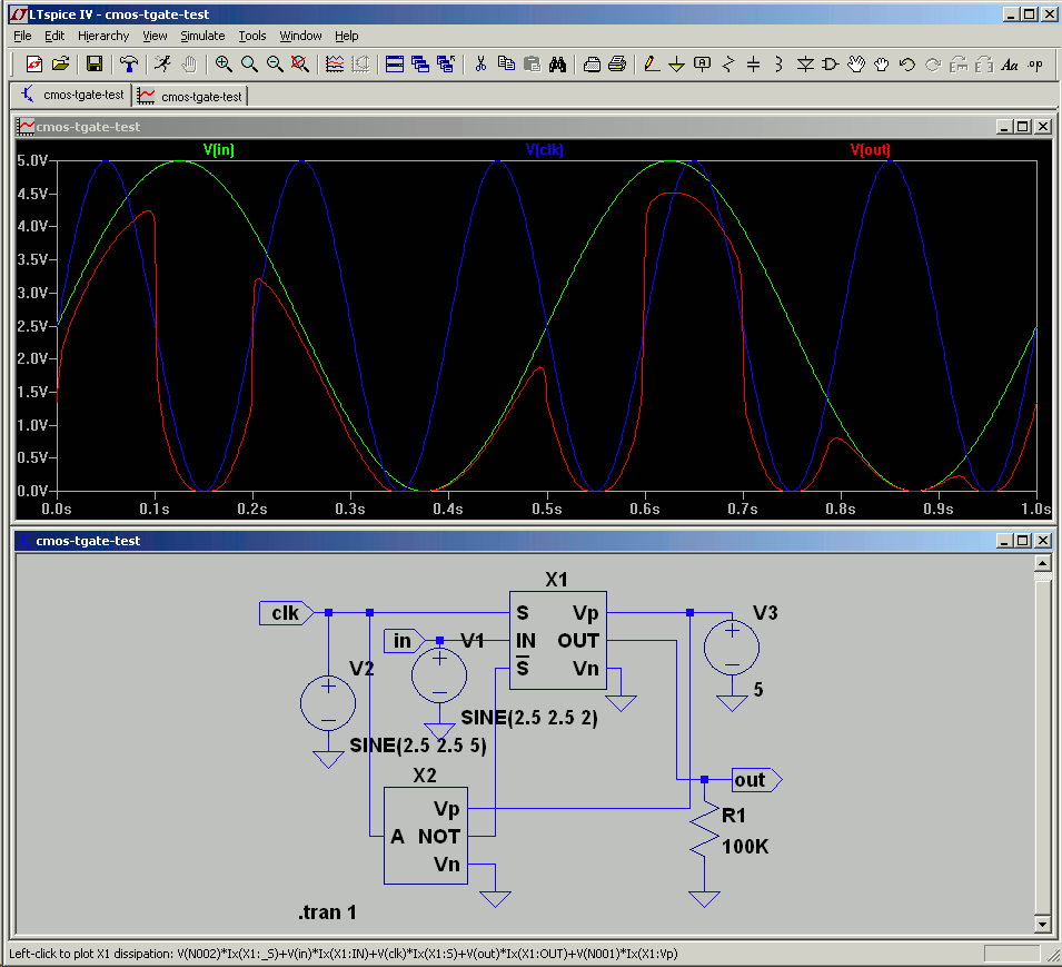
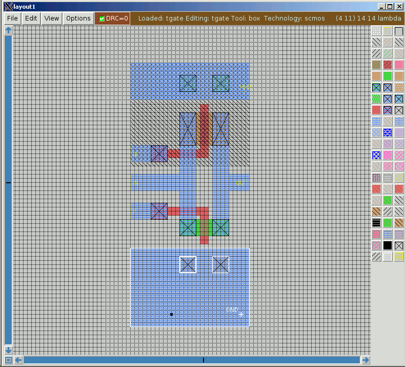
CMOS transmission gate
10/03/2016 at 04:20 • 0 commentsLTSpiceIV model:
![]()
Test circuit for LTSPiceIV:
![]()
Magic layout:
![]()
Shared Silicon
Silicon proven way to reduce the cost of integrated circuit manufacturing by collaboration


 So one ternary selector has: