Ted Yapo
-
Two diode latch
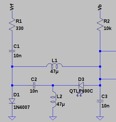
12/07/2017 at 18:22 • 1 commentI was reading about the #One Transistor Latch project and it reminded me that I came up with a two diode latch at one point. Here's the idea (note that the diodes are labeled D1 and D3, even though there are only two of them):
![]()
Like the DDL logic gates, it uses both RF and DC bias power supplies. D1, a 1N4007 rectifier, is used as a PIN switch, while D3, an LED, serves as a rectifier and state indicator.
In the "0" state, DC bias current flows through R2 and L1 to bias D1 into a conducting state. As in a PIN diode, this forward bias makes the diode present a low impedance for RF current, so RF current through R1 and C1 is shunted to ground through D1.
If we momentarily disconnect the DC bias supply, Vb, D1 stops conducting, and begins to show a high impedance at RF. Now, RF energy flows through R1, C1, and C2, to become rectified by D3, charging C3 to a negative voltage. This negative voltage reverse-biases D1, maintaining its high impedance at RF. Even if we now reconnect the DC bias supply, the rectified current is enough to offset the bias through R2, so the "1" state is maintained. While D3 is rectifying current, it emits a nice glow to indicate the "1" state.
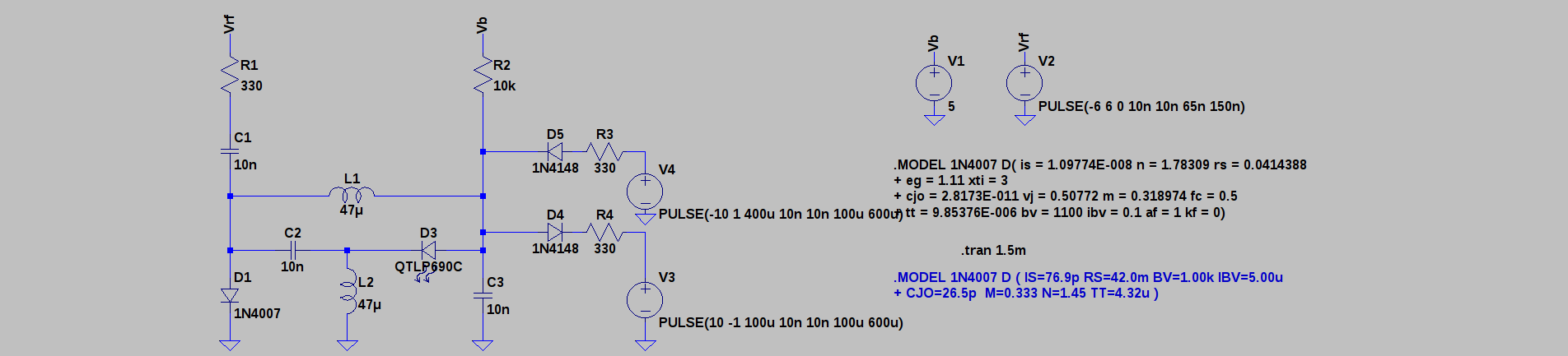
You could also set the state with some switches that temporarily shorted R1 or R2 to ground. This might make for an interesting demo circuit. In simulation, I chose to use two more diodes to switch the state. Here, D4 and D5 alternately switch the latch state based on their respective pulse generators:
![]()
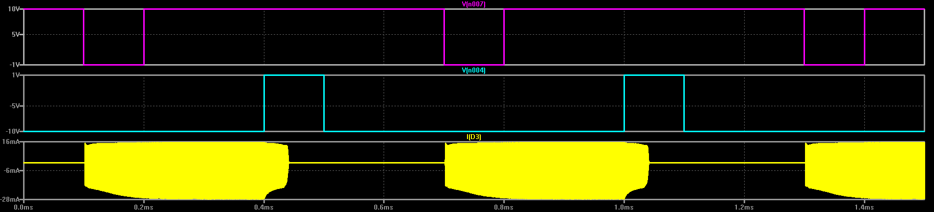
Here, you can see how the pulses set the latch state:
![]()
The top trace (magenta) sets the "1" state with a low-going pulse through D4. This causes D3 to start rectifying current, shown in yellow. This state continues until a positive-going pulse through D5 flips the state so that D1 starts conducting again, which stops current through the LED.
Is it practical? Probably not. But I think it's pretty interesting that you can store a bit of information in two diodes and a handful of passives.
-
SRAM Cell
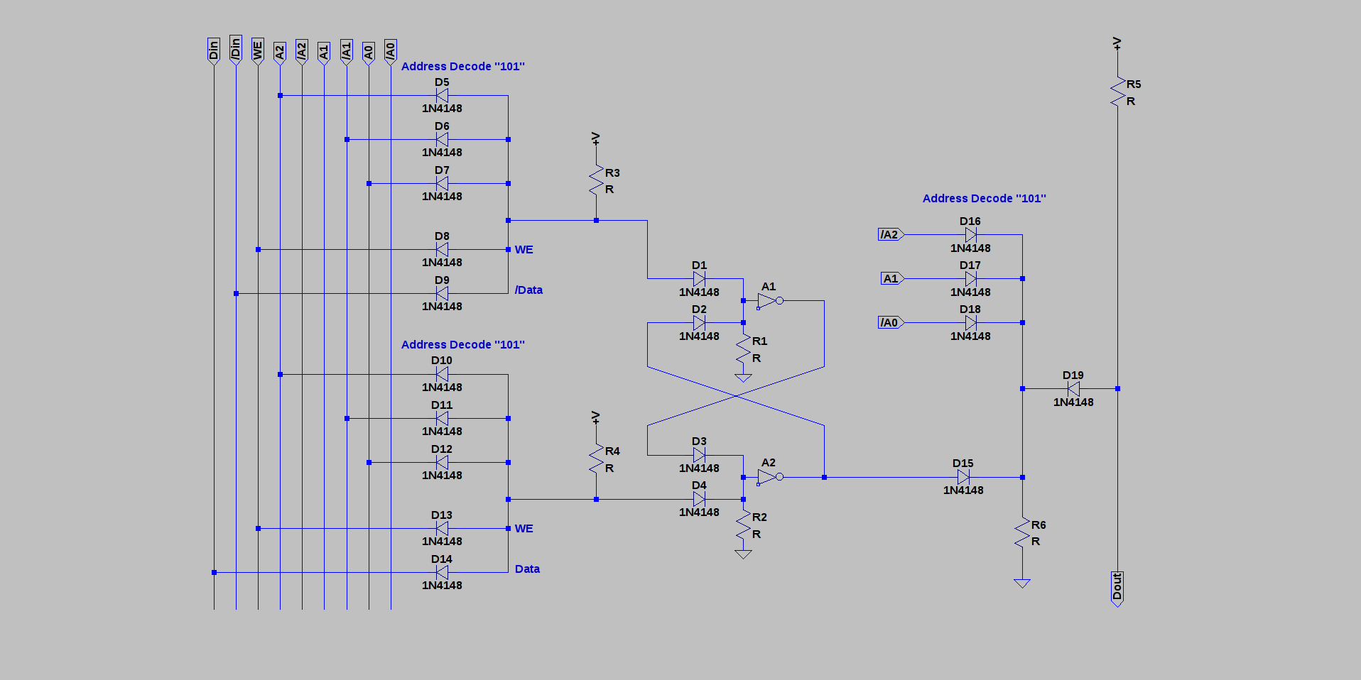
02/07/2017 at 18:00 • 0 commentsThere was a mostly-diode SRAM cell design on nanocpu.org (documented here as #NanoCPU.org); I think it's undergoing some renovations at the moment, but I wanted to cite it because it was definitely what got me thinking about diode-based SRAMs again. Here's my take on the same concept - a single-bit SRAM cell using a two-inverter latch as the storage element. All the address decoding and R/W logic is done with diode AND/OR cascades - both for the input and output. This particular version decodes 3 address lines; so it would be suitable for an 8-address memory.
![]()
As with the other designs, both true and complemented address and data lines are required - this costs a few inverters, but this cost is amortized over the number of storage cells. For N address lines, this design requires 3N+10 diodes per bit (less if the latch diodes are built into NOR gates, for example). You can reduce this somewhat if you allow two levels of AND diodes; then the write address decode can be done once, reducing the number of diodes to 2N+10 per bit. This may or may not be a good trade-off depending on what you are using for inverters. I'll have to think about whether this can be made to work with DDL inverters, or if I have to use all the diodes.
Note that the output logic uses inverted levels so that it doesn't affect the latch; when I first uploaded the schematic, I had it backwards: it's an easy mistake to make. Since the latch has both true and complemented outputs available, it's easy enough to use the opposite output to drive inverted output logic.
As with the previous ideas along these lines, fan-out will limit the number of cells that can be used without buffering on the address and data lines. Even so, this seems like a decent storage architecture for a diode-only CPU. My previous thoughts had each bit of storage taking a whole DDL01 board (six gates). With this mostly-passive-diode idea, the density improves to store 3 bits per board (plus a bunch of diodes to put somewhere).
-
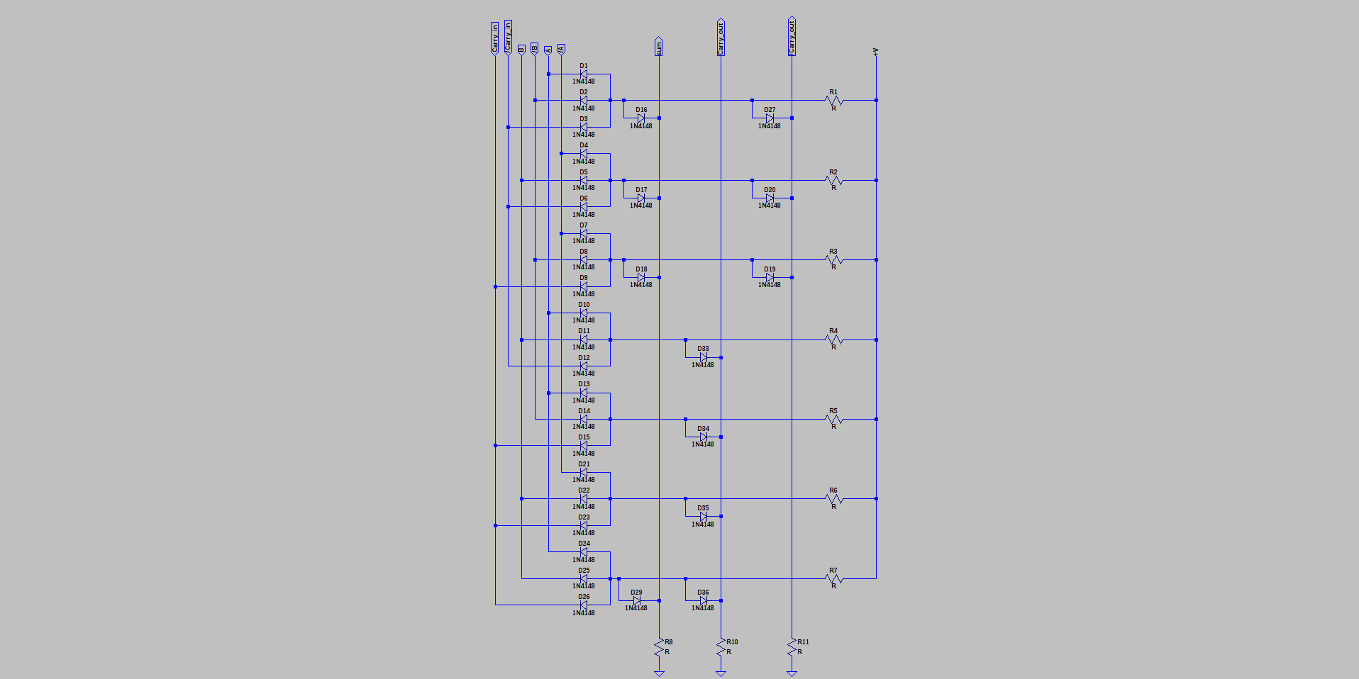
Diode Full Adder
02/07/2017 at 17:05 • 0 commentsOf course, if you can do anything with the two-level diode sum-of-products formulation, you can do anything. Here's a shot at a full adder:
![]()
It requires inverted and true inputs for A, B, and CarryIn, and output buffers for Sum, CarryOut and /CarryOut, but that's only 6 inverters. A quick try with NOR gates used 12. With six inverters, it only requires a single DDL01 board per bit in a ripple-carry adder. That's not bad at all. Of course, there's no reason you need to limit the active devices to just diodes, either. Simple transistor inverters would work here, as would relays or other amplifier/inverters, if you're into that kind of thing.
The operation is simple. The sum output is high if any single one of the inputs is high (three product terms) or if all three are (one product term). The carry output is high if any two or three of the inputs is high (four product terms). An inverted carry out is computed, too, because it's cheaper and faster to do it here than adding another inverter in series to the normal carry output.
I've convinced myself that with DDL, whose clock speeds are in the low kHz region, the speed of these cascaded diode gates are not an issue, and will greatly simplify and speed construction of a simple CPU. With faster technologies, you would have to re-evaluate this decision.
This full adder circuit can be connected to form a ripple-carry adder very easily, but there's no reason that a carry-lookahead circuit can't be constructed with the same AND/OR cascade. Maybe a 4-bit lookahead would strike a good balance between speed and number of components. I'll have to take a look at it.
-
Project back from the dead
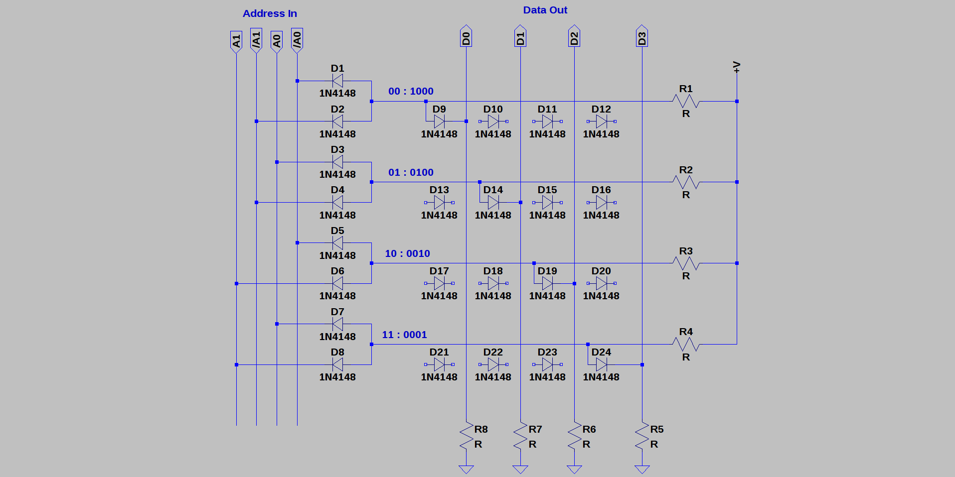
02/06/2017 at 18:41 • 3 commentsIt's nearly springtime, when a middle-aged man's fancy lightly turns towards thoughts of computers constructed from diodes... Seeing some recent posts (I'll have to look around for the links) made me finally realize that 2-stage diode logic gates with AND followed by OR is functionally identical to the AND/OR matrix found inside PALs, GALs, PROMs, and all the other simple programmable logic out there. See the diagrams on this page for details. In fact, the sum-of-products computed by this AND/OR cascade can compute any function of the input variables. I don't know why it took me so long to realize it. Using this formulation, a ROM with diode-decoded address lines looks like this:
![]()
It's a 16-bit ROM of four words of four bits each. An inverted version of each address line is required as an input. I only connected one diode for each word, but you can get the idea. The inputs are required to sink current, which means reversing the output diodes on DDL gates, but that's very easy to do. You need to choose (or eliminate) the pull-up/pull-down resistors depending on the logic circuits you use to drive/read this array.
The main problem with this kind of implementation is fan-out. Each address line may be required to pull down a resistor for each word, which could add up quickly. In a practical implementation, address line buffers might be required for every N words - maybe a PCB with the buffers and some power-of-2 words could be made - like a 32-word ROM board.
Anyway, I finally "got it" with the AND/OR cascade of diode gates. It took long enough :-)
Now, we need a RAM with a similar design...
Diodes Only
A community project to explore diodes as active devices. Collaborators welcome; leave your transistors at the door.