-
The New Model
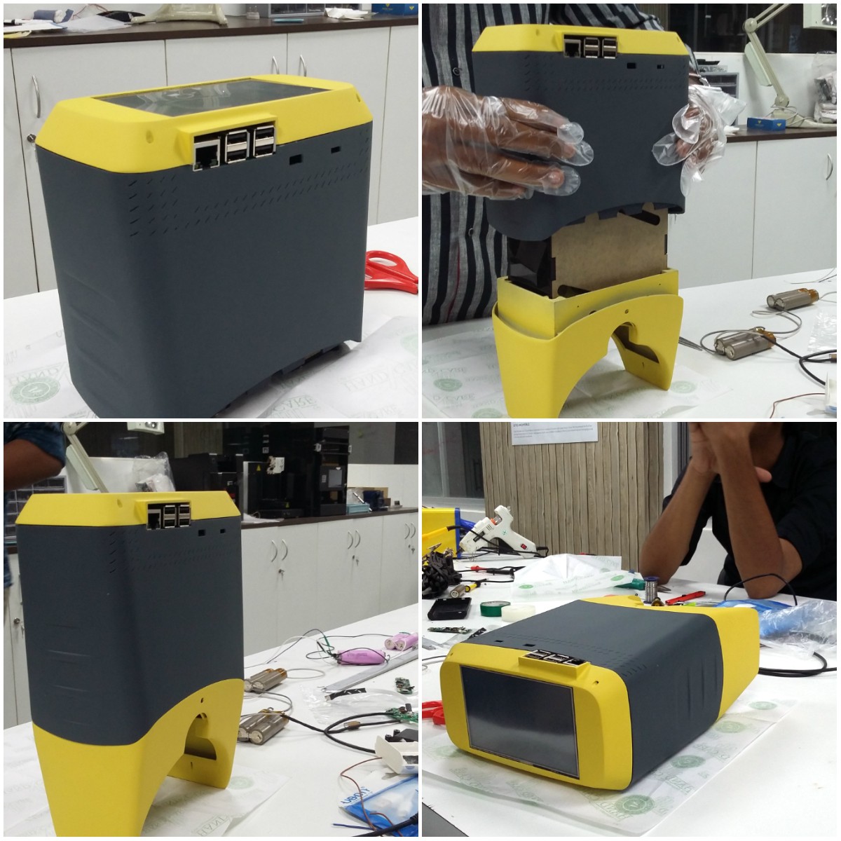
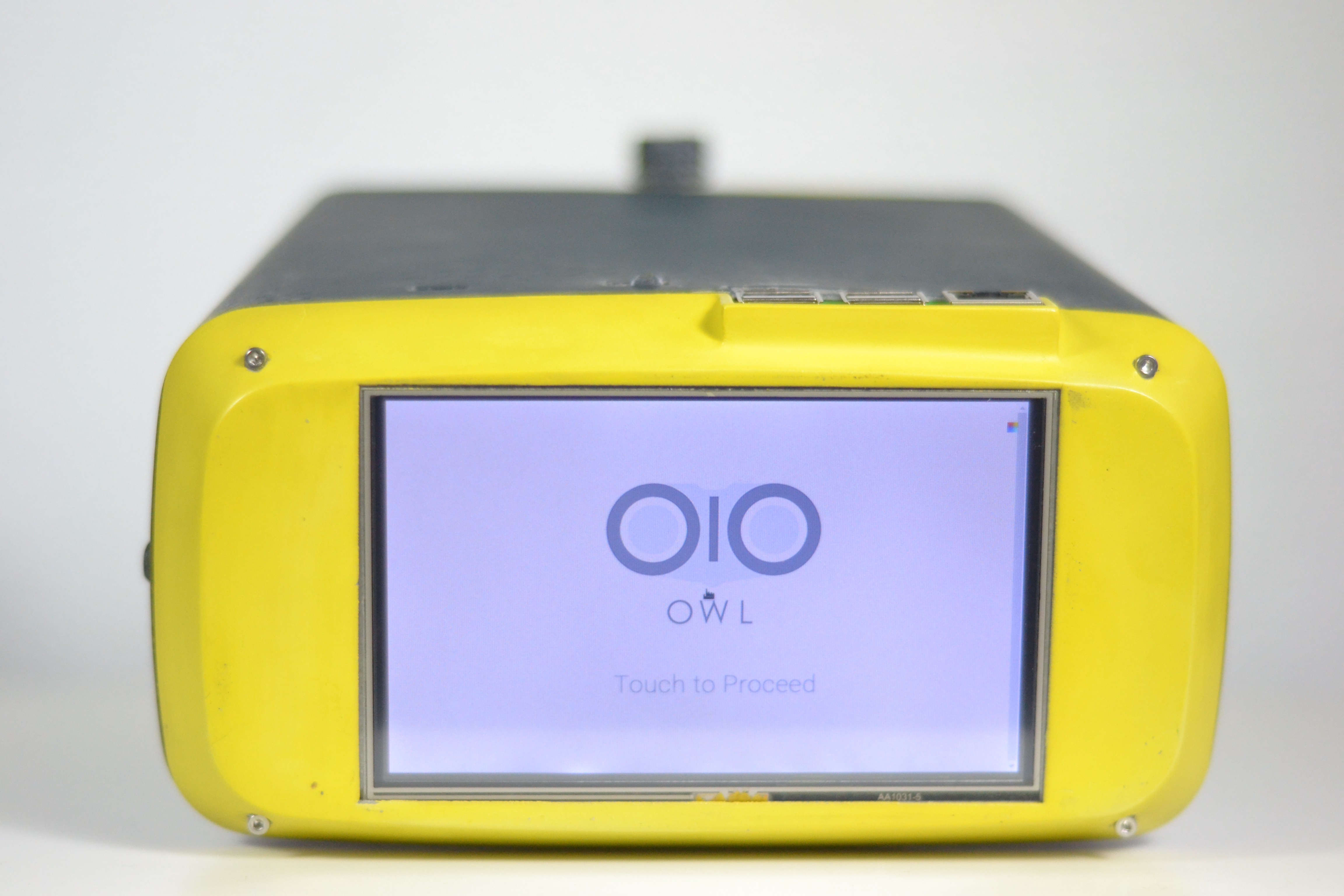
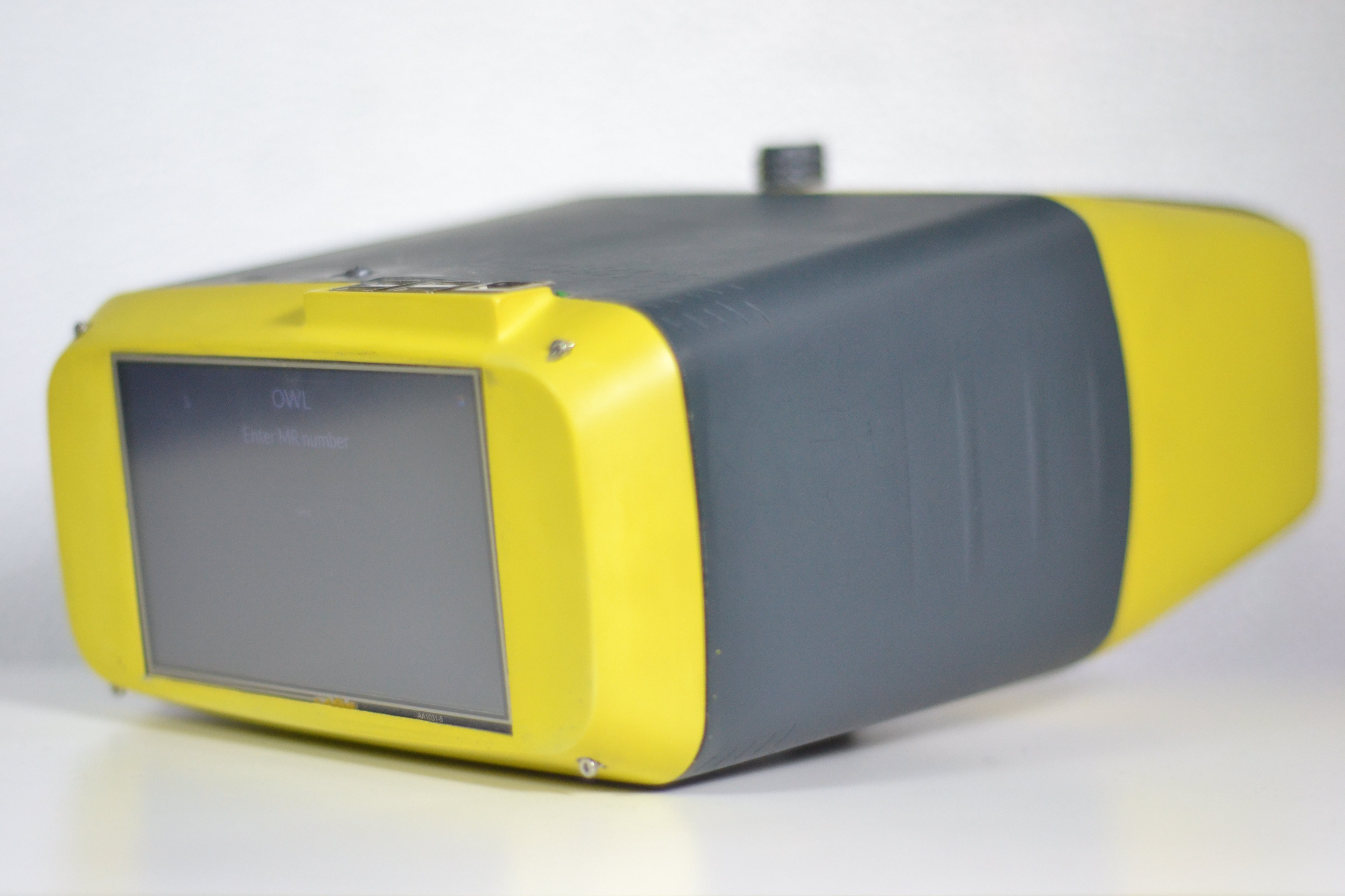
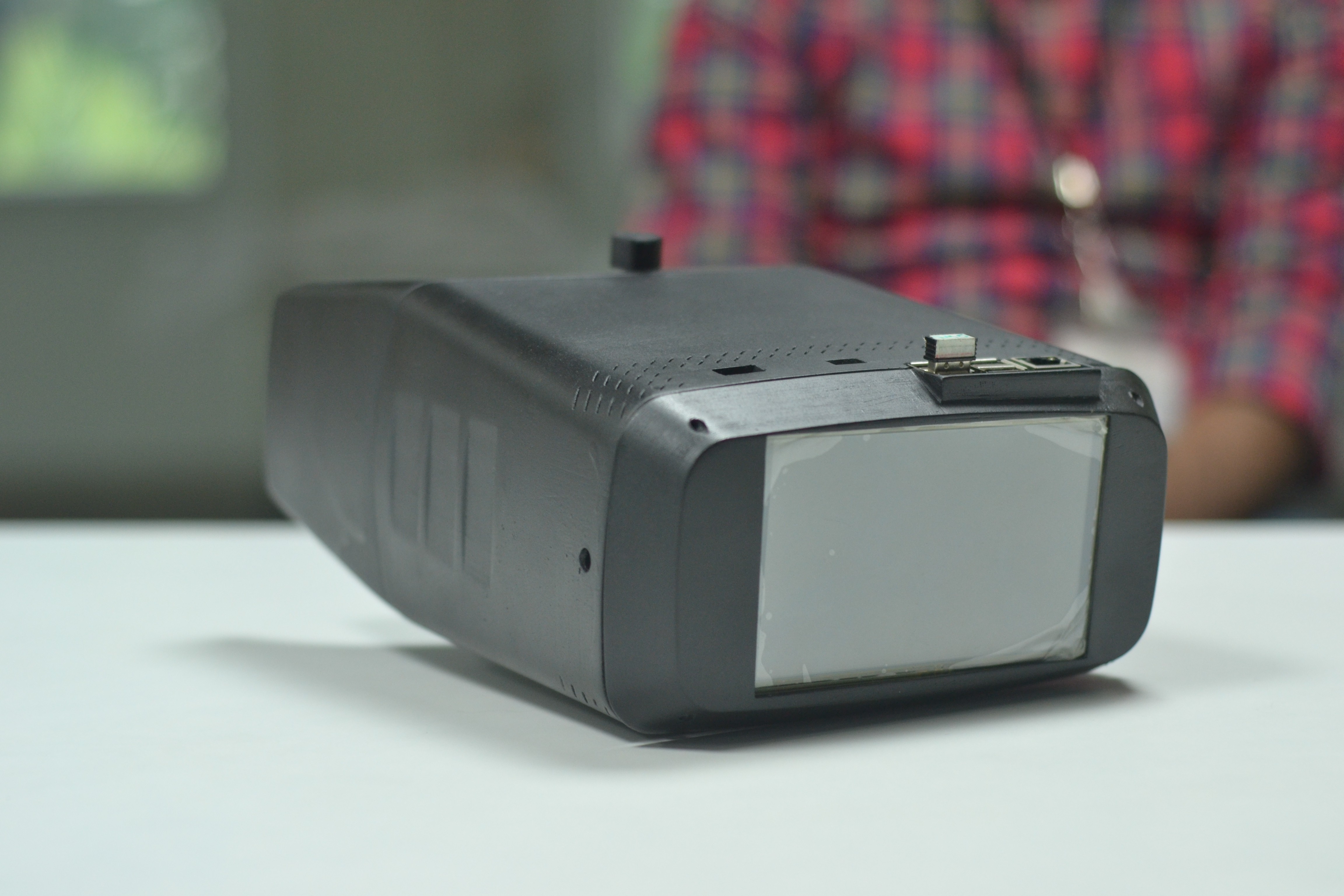
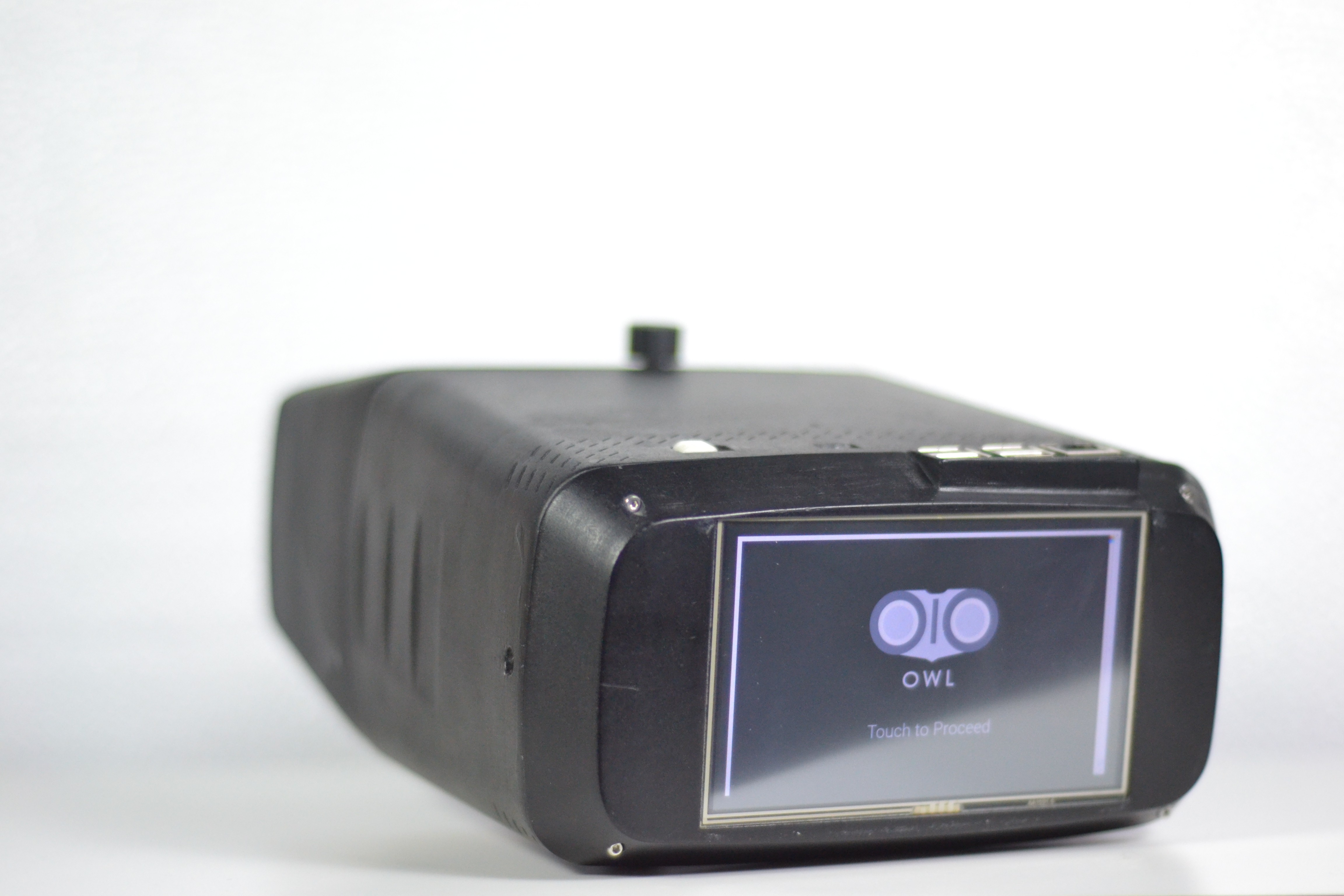
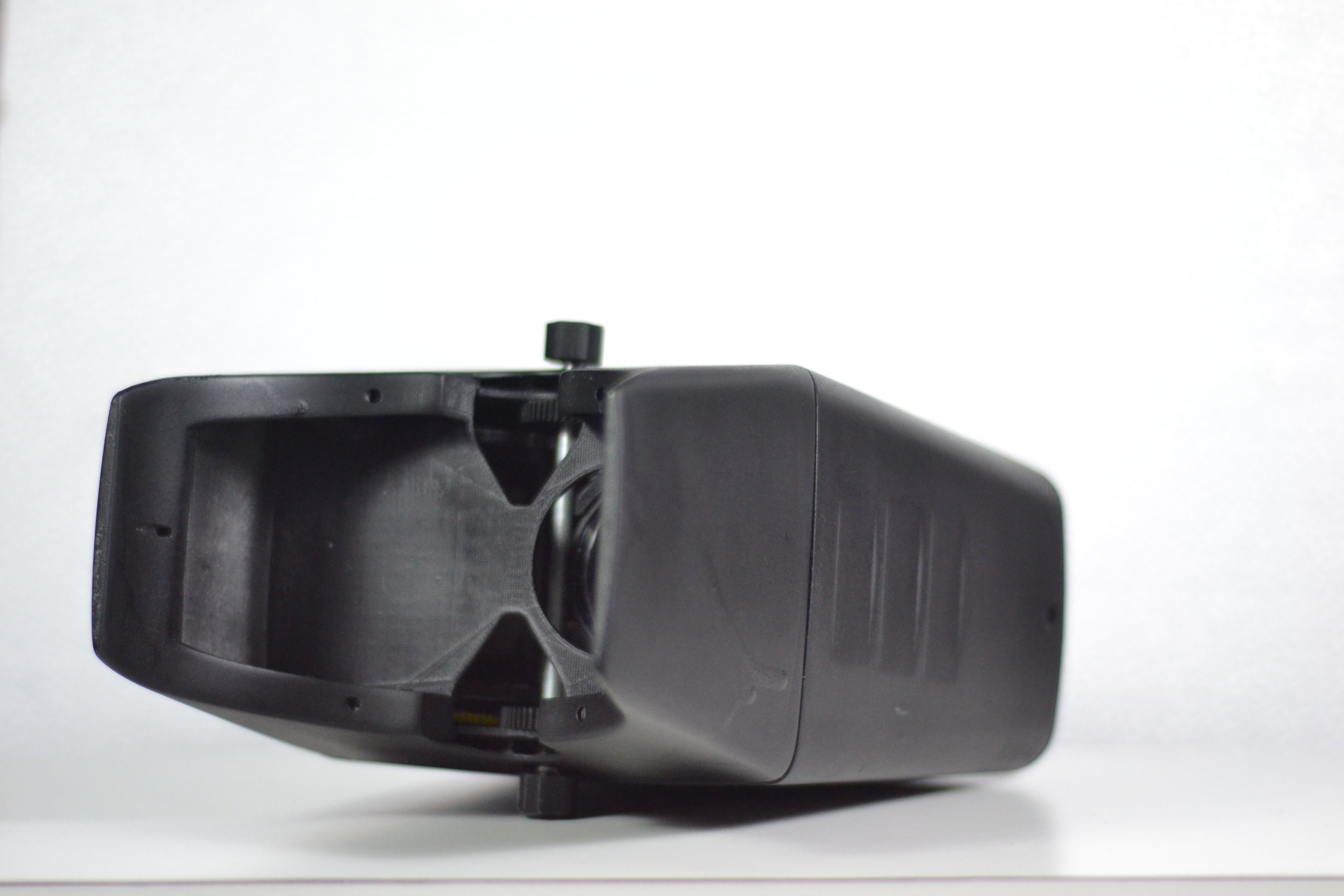
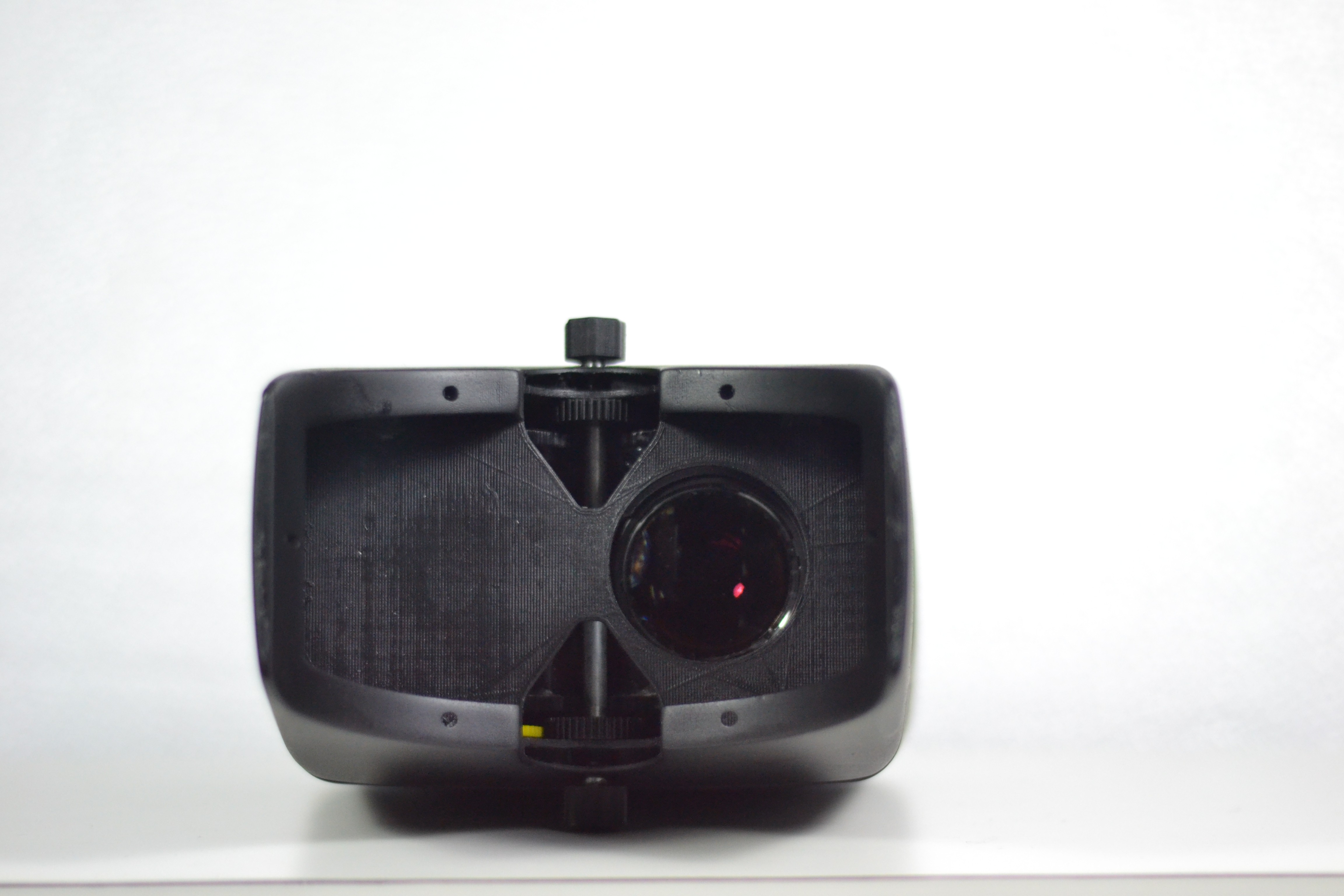
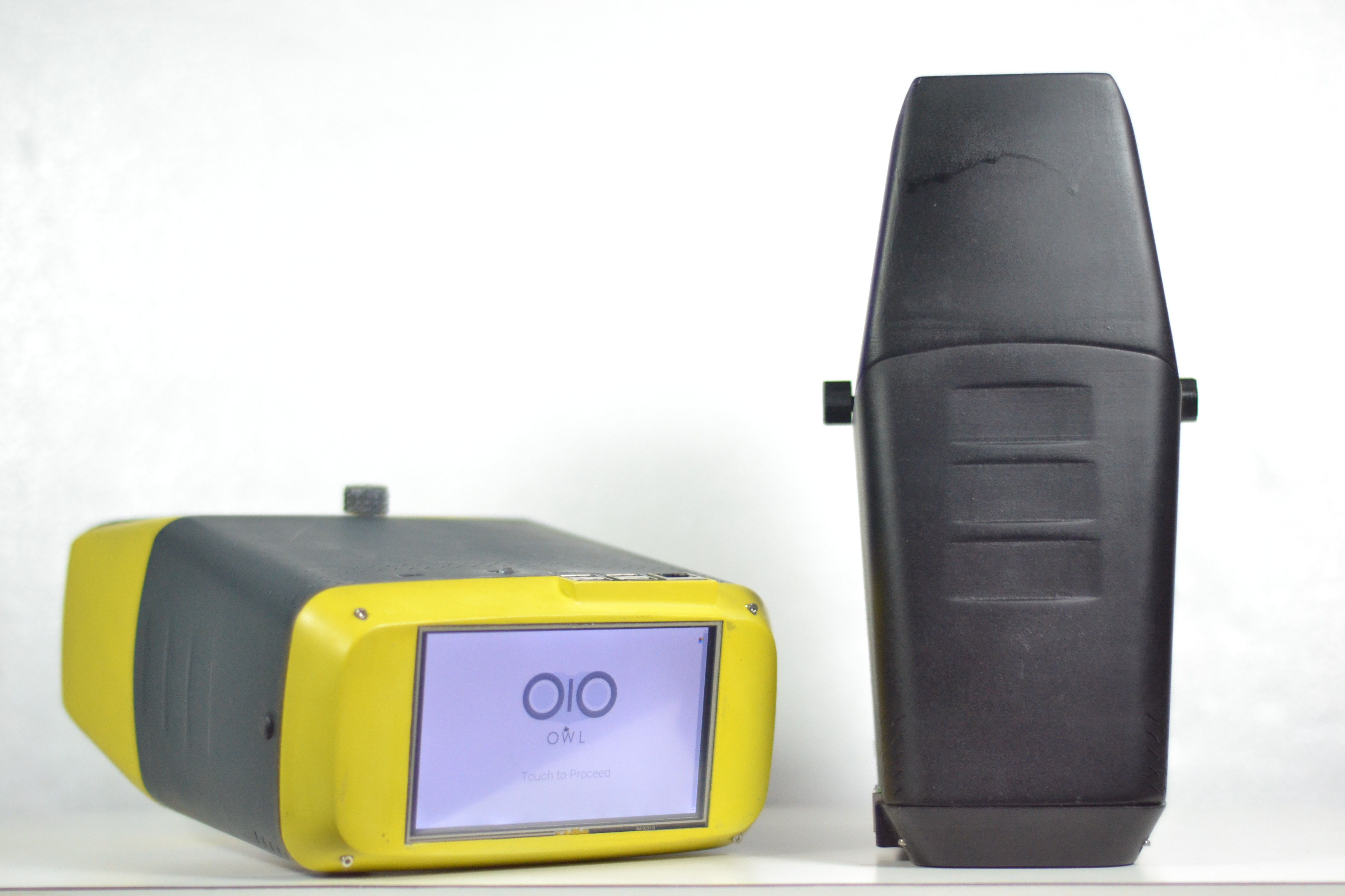
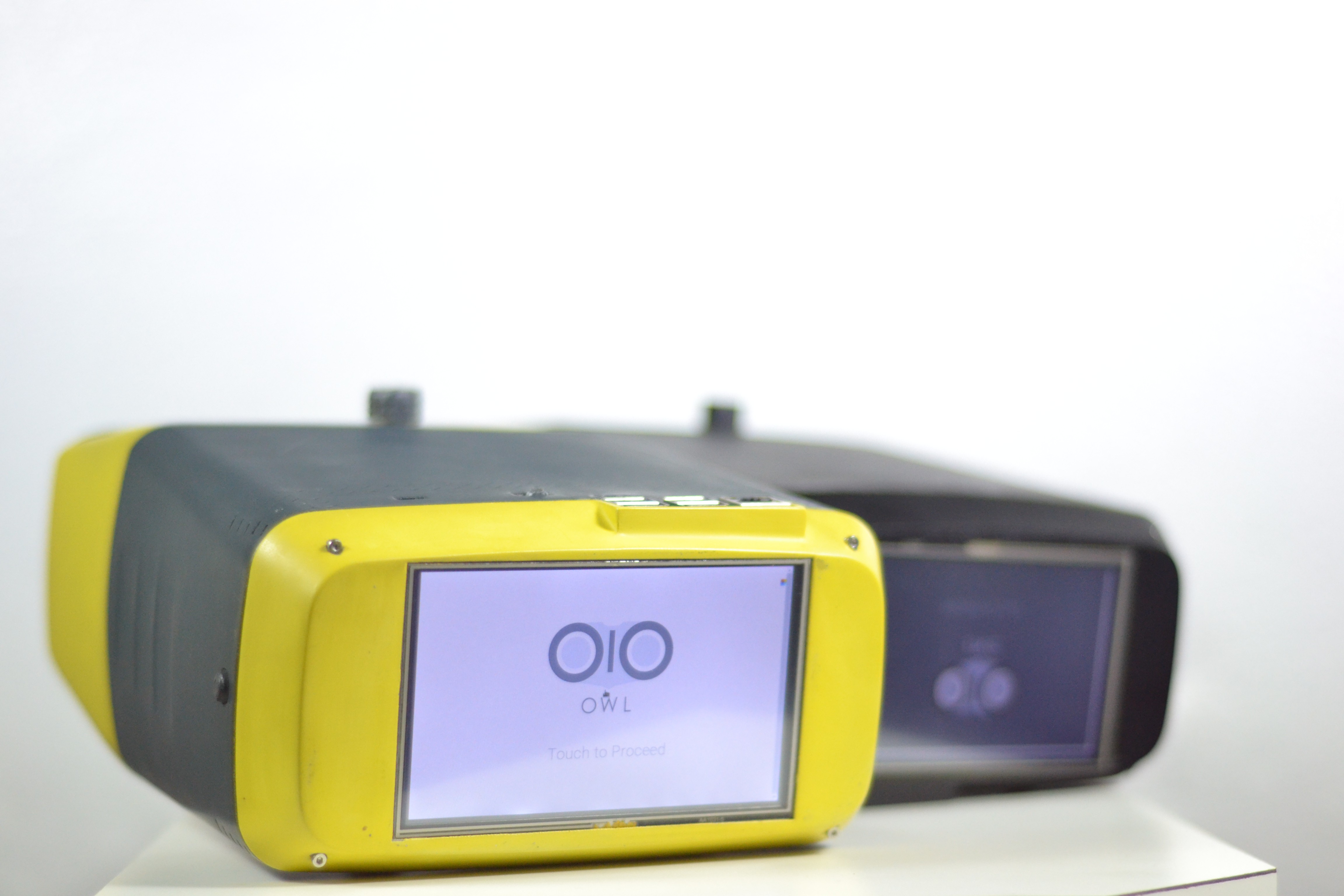
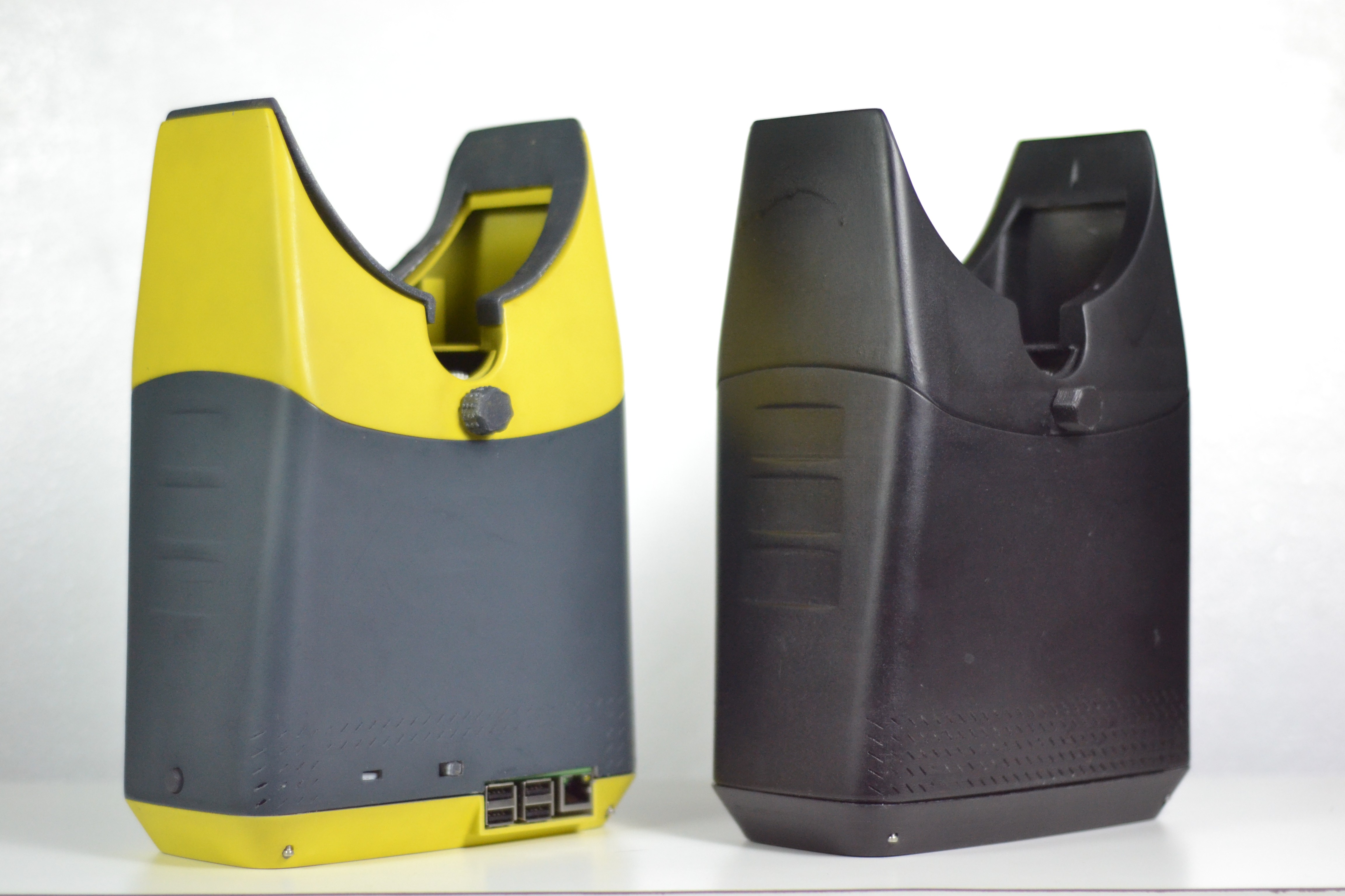
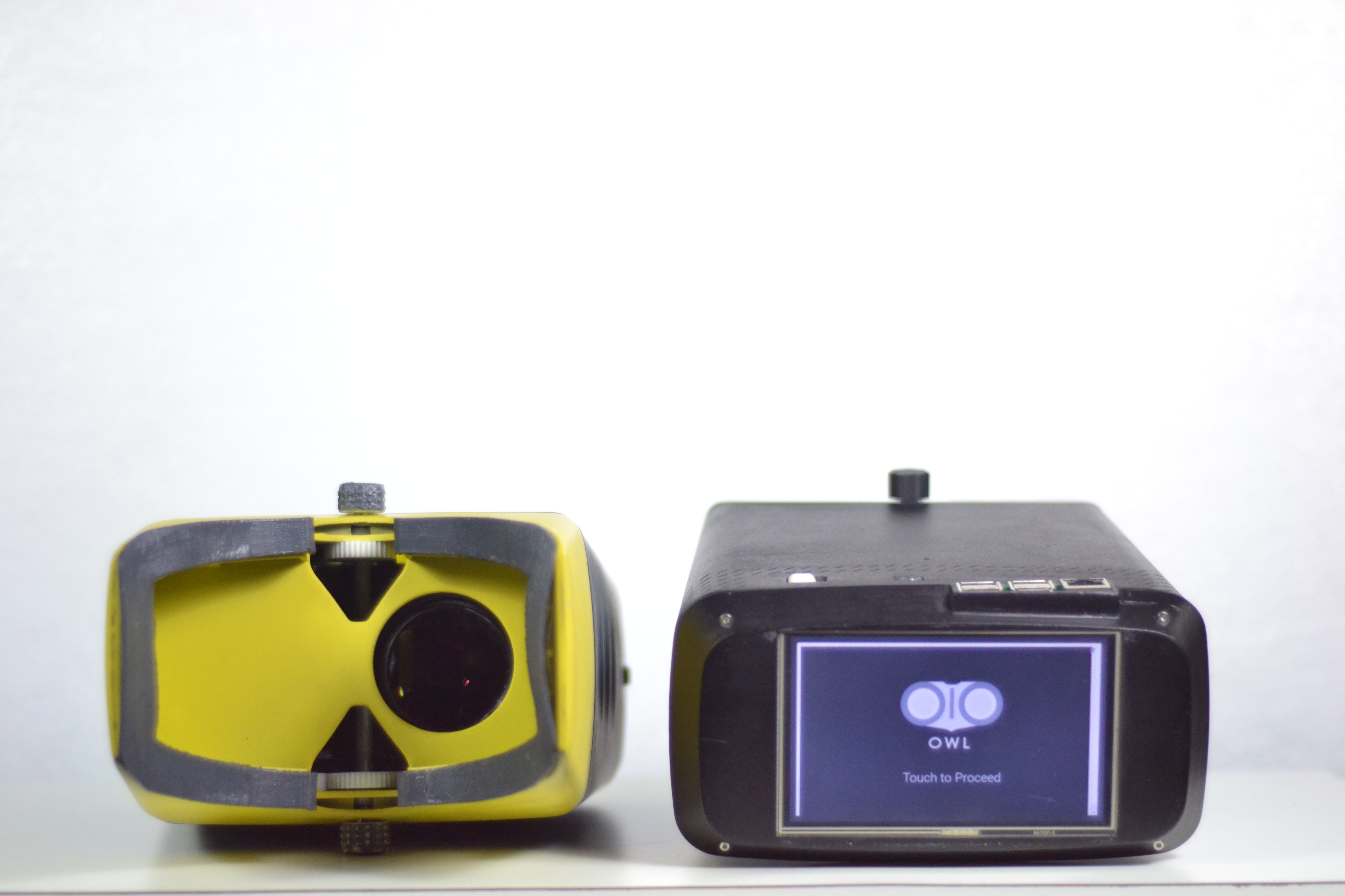
10/07/2016 at 14:49 • 0 commentsThe design models have been 3D printed and assembled. We made two devices, only the outer casings are different in the two models. One is printed on a SLS 3d printer (Nylon PA-12) and another one with an FDM 3D printer (PLA Black).
Both the models are working fine and were able to capture decent retinal images.
The SLS printed outer casing for OIO
![]()
The PLA printed and matte black painted OIO device
![]()
Assembled Devices
![]()
-
Design Considerations
10/07/2016 at 12:37 • 0 commentsEarlier version of the device was reconsidered in terms of following aspects:
• Accommodating for different refractive errors
• Aesthetics
• Ergonomics
• Weight distribution
OIO
![]()
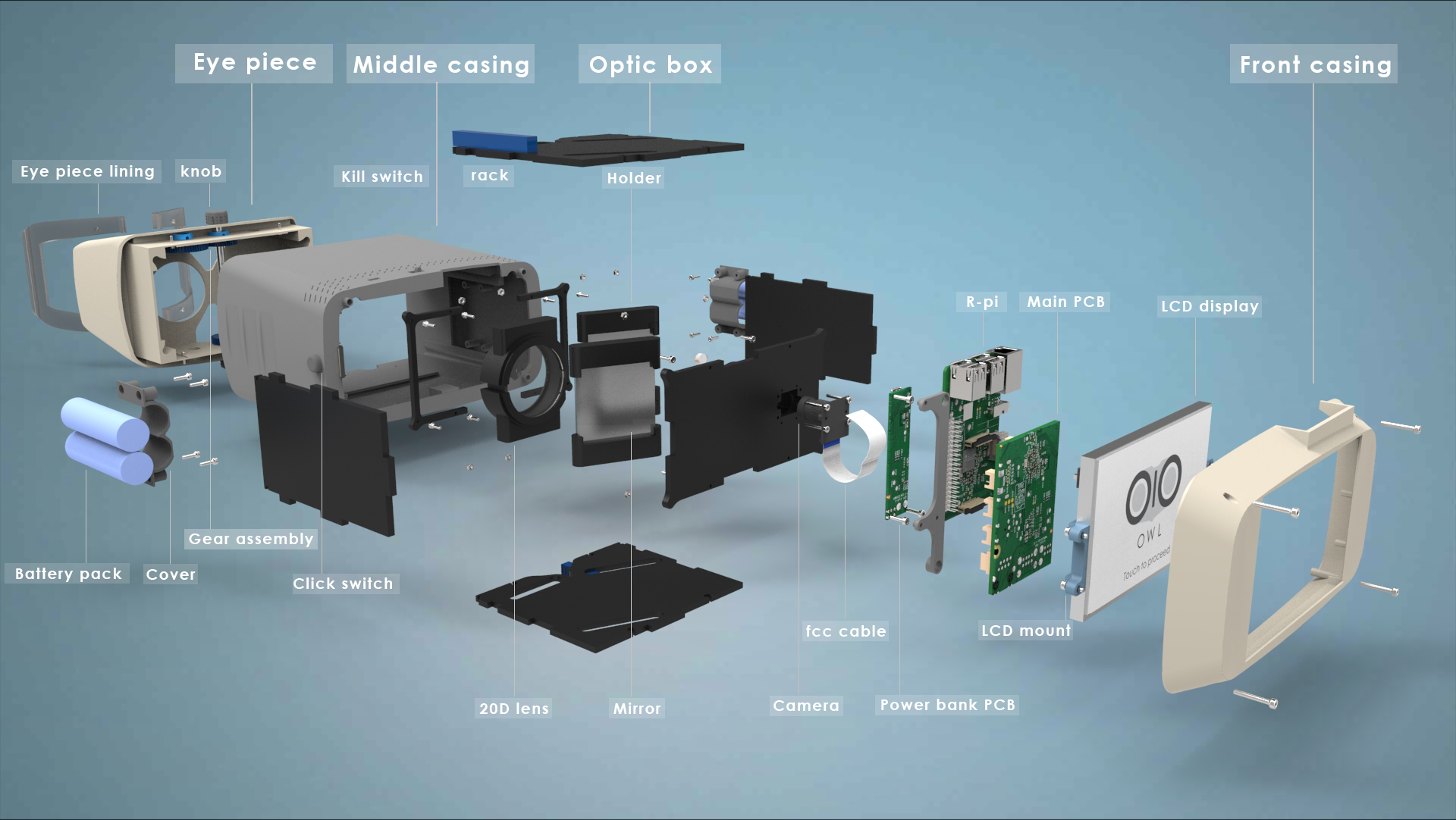
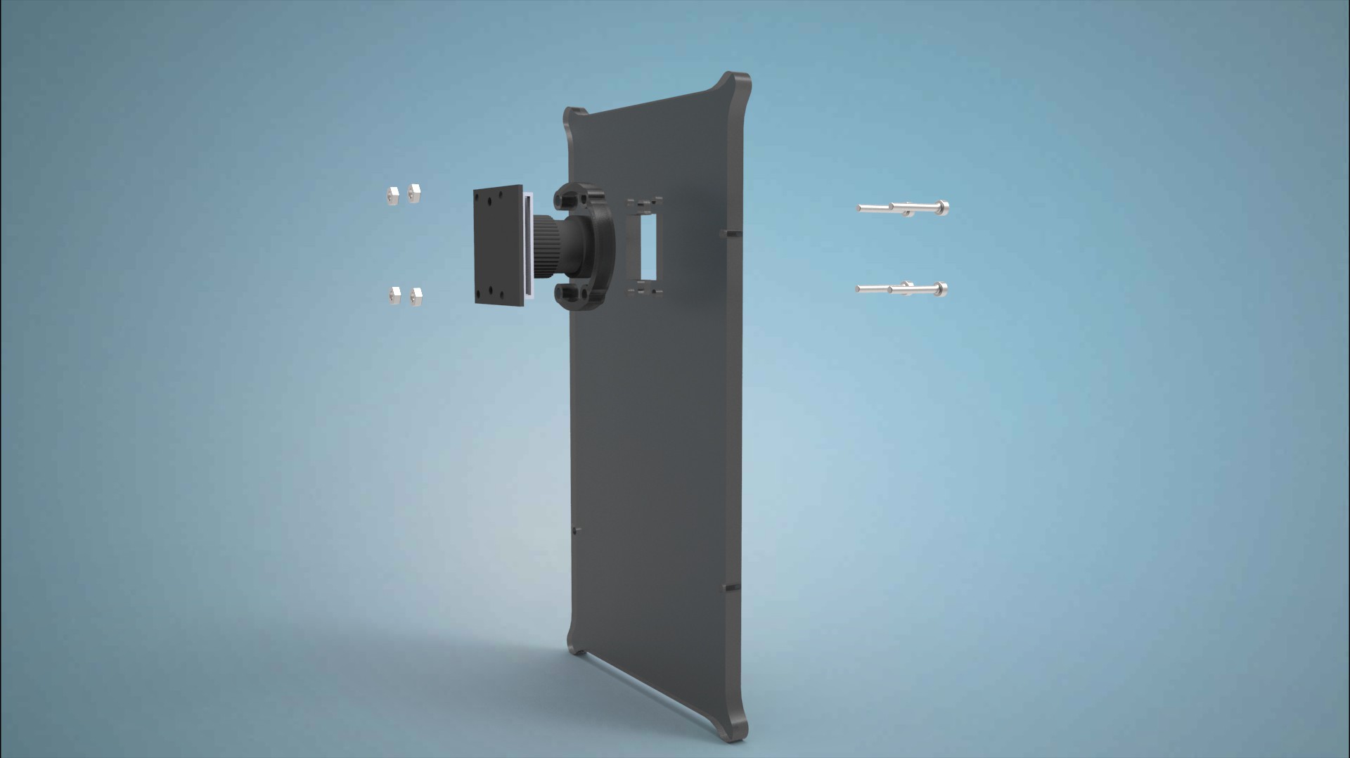
ASSEMBLY
![]()
EXPLODED ASSEMBLY
1. ACCOMMODATING FOR DIFFERENT REFRACTIVE ERRORS
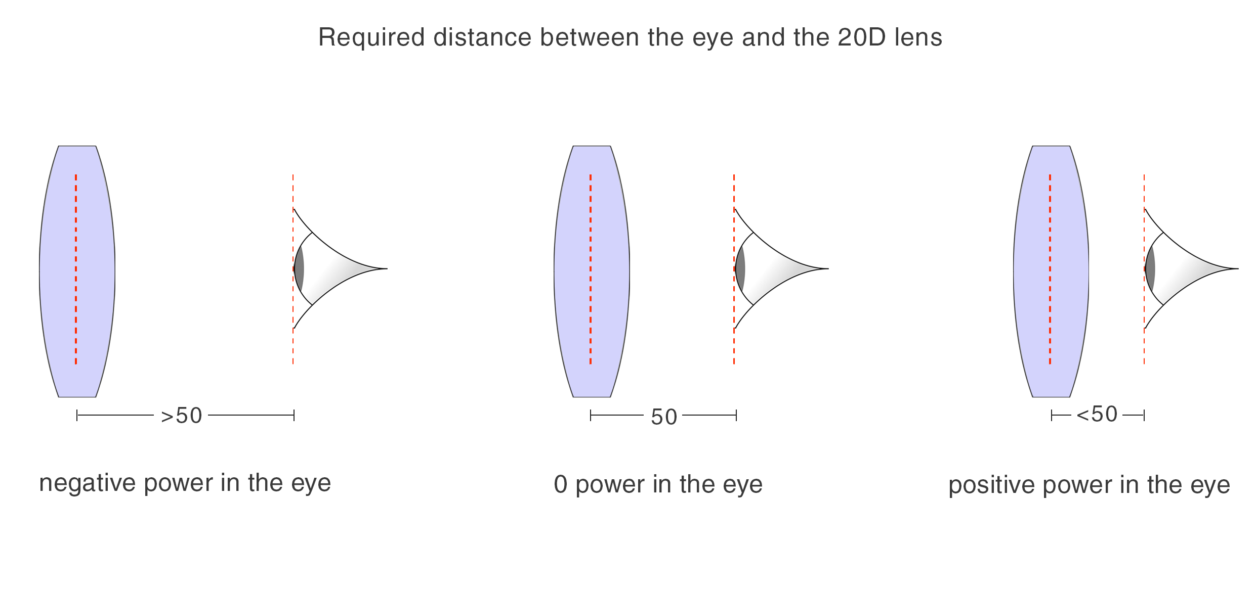
For different people with varying refractive errors, focal length for the 20D lens changes.
For an eye with normal refractive error, the distance between the 20 D lens and the eye has to be 50mm for a focused image of the fundus.
For people with negative errors, the distance goes on increasing and for people with positive refractive errors, the distance goes on increasing.
![]()
BEFORE
![]()
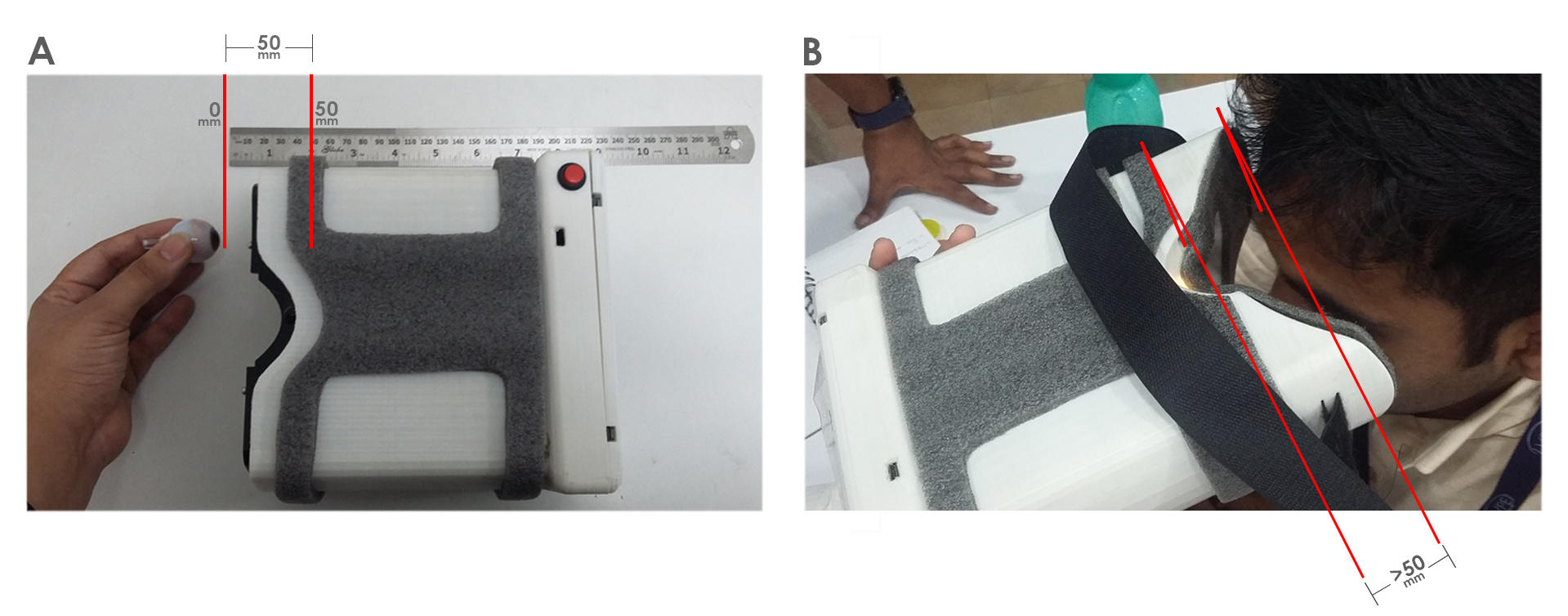
A. In the earlier iteration,the optic box was fixed at particular position such that the distance between the eye and the 20D lens was 50mm.
B. Position of the device with respect to the patient's eye with a negative refractive error (power) . As the person has some negative error, the distance between the eye and the 20D lens is more than 50mm. Hence the device has to be held away from the face to increase the distance.
AFTER
![]()
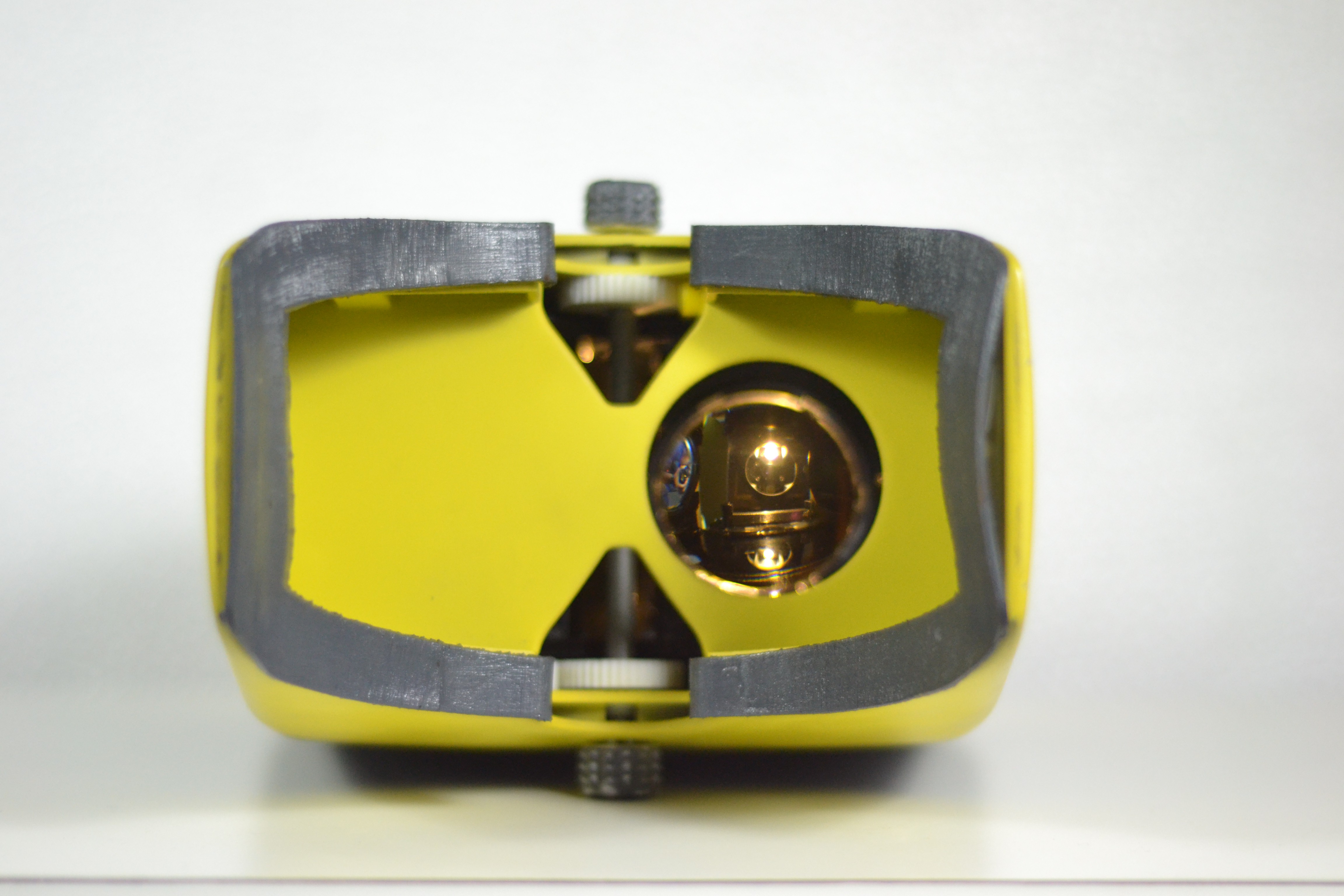
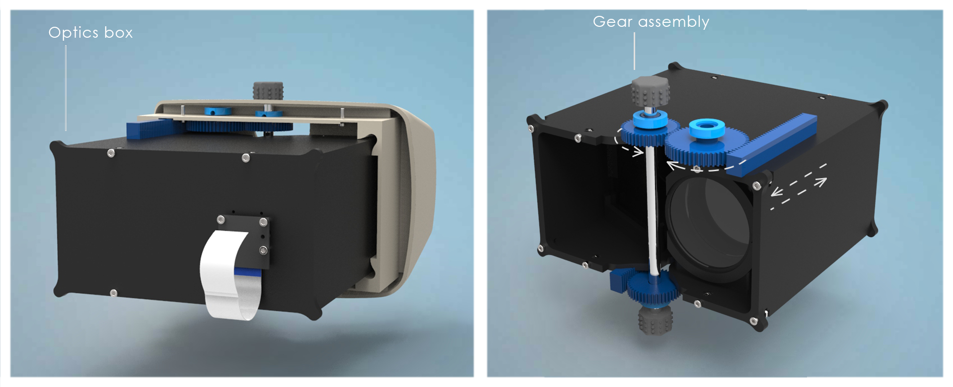
The optic box moves back and forth inside the device by means of sliders which are integrated as a part of the eye piece and the middle housing.
The box moves by the means of a rack and pinion assembly.
![]()
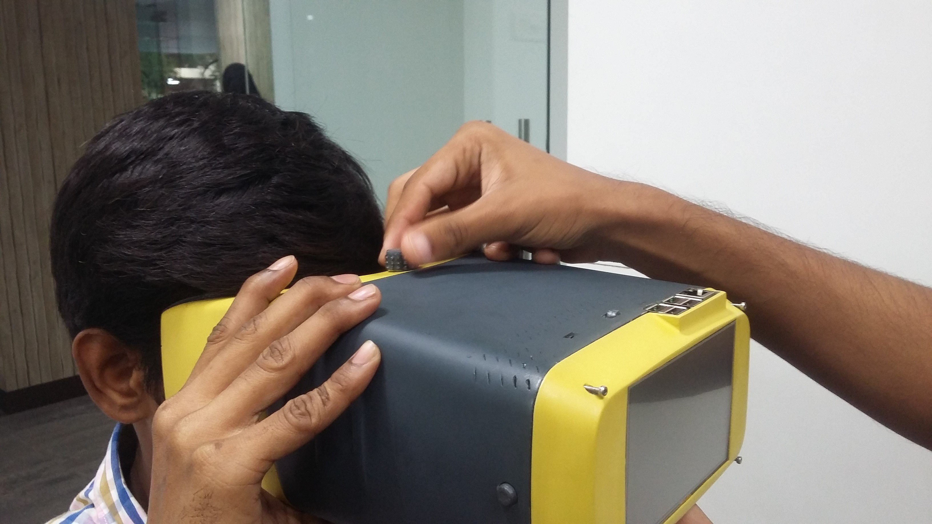
The distance between the eye and the lens can be adjusted by rotating the knob as in the image above.
2. AESTHETICS
The meaning that the appearance of a product communicates helps consumers to assess the product on functional, aesthetic, symbolic or ergonomic motives in this case a medical setting.
A. COLOR and MATERIAL
![]()
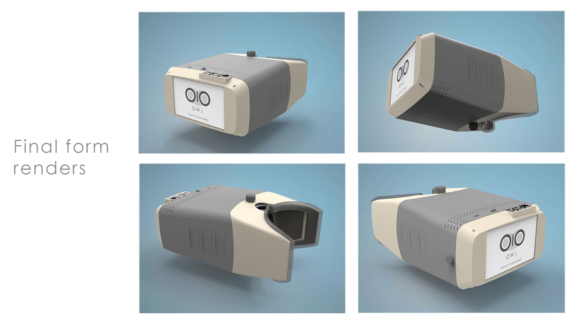
The subtle colors used, grey and beige, are suitable for a medical device. These colors have a calming effect on the patients.
![]()
The material used is medical grade and is safe for use.
The part of the eye piece which comes in contact with human skin has been made out of silicone. Thus it can be cleaned with alcohol swabs after every testing.
B. FORM FEATURES
The physical appearance or form makes the device look safe and easy to use.The basic aesthetics including contours and curves tend to make the product intuitive for the end user.
![]()
![]()
![]() There are suggestive grips provided at strategic places on both sides to ensure correct handling and positioning.
There are suggestive grips provided at strategic places on both sides to ensure correct handling and positioning.These provide a clear boundary between the interaction of the patient with the device and the clinician with the device.
The heat sinks provided on the outer housing near the R-pi add to the aesthetics of the device.
3. ERGONOMICS
![]()
![]()
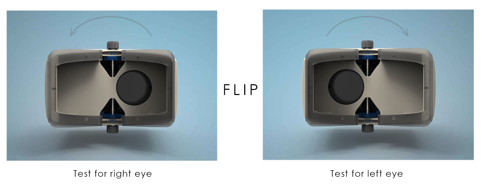
A.Symmetry along horizontal axis
The device has to be symmetric along the horizontal axis.
This is because only one eye is to be tested at a particular instance.
The cavity near the other eye is closed . To test the other eye, the device has to be flipped.
![]()
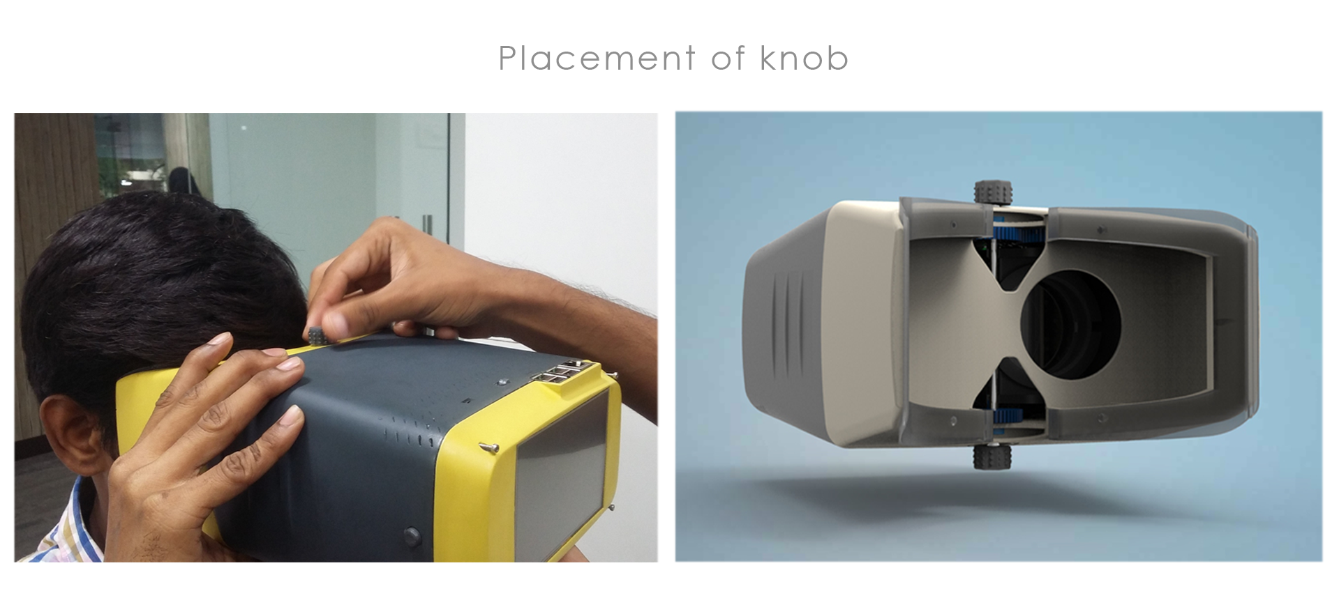
B.PLACEMENT OF SWITCHES AND KNOBS
![]()
The click switch is placed ergonomically at the side of the device.Thus, image can be captured for both the eyes by flipping the device.
![]()
The knobs for moving the optic box are placed at center bottom and center top of the device with a rod connecting the two
C. ERGONOMIC EYE PIECE
The eye piece plays the most important role in the device.
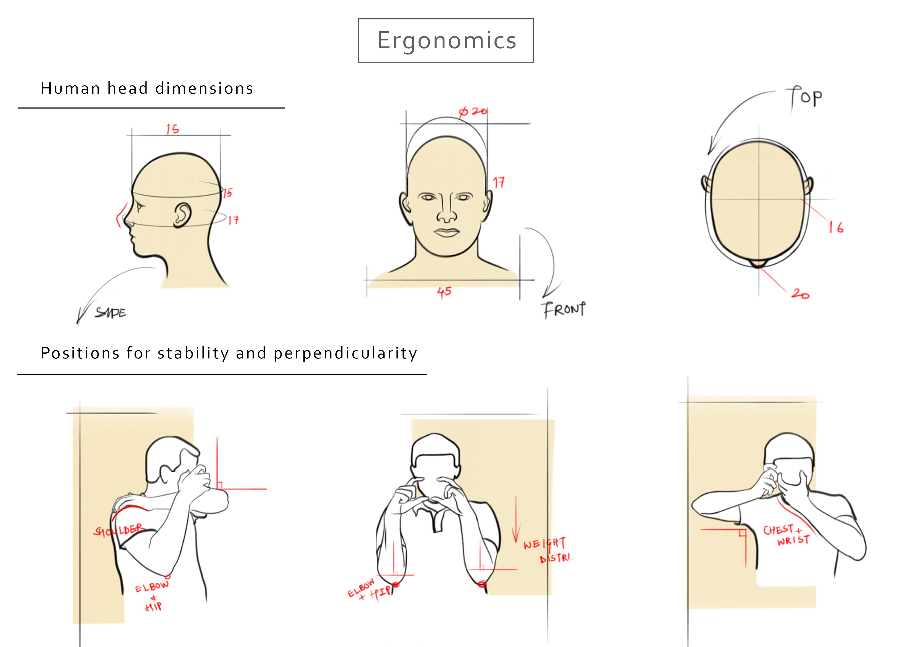
In a conventional fundus camera, the face of the patient is held steady by means of a chin support and the camera lens is placed perpendicular to the face setting.
As OWL is a hand held device ,holding the device perpendicular to the face plane was quite a task. If the device is not held perpendicular, only partial fundus can be observed.
Hence, the eyepiece had to be designed in such a way that it is a 95 percentile ergonomic fit and aligns perfectly onto the face perpendicularly.
![]()
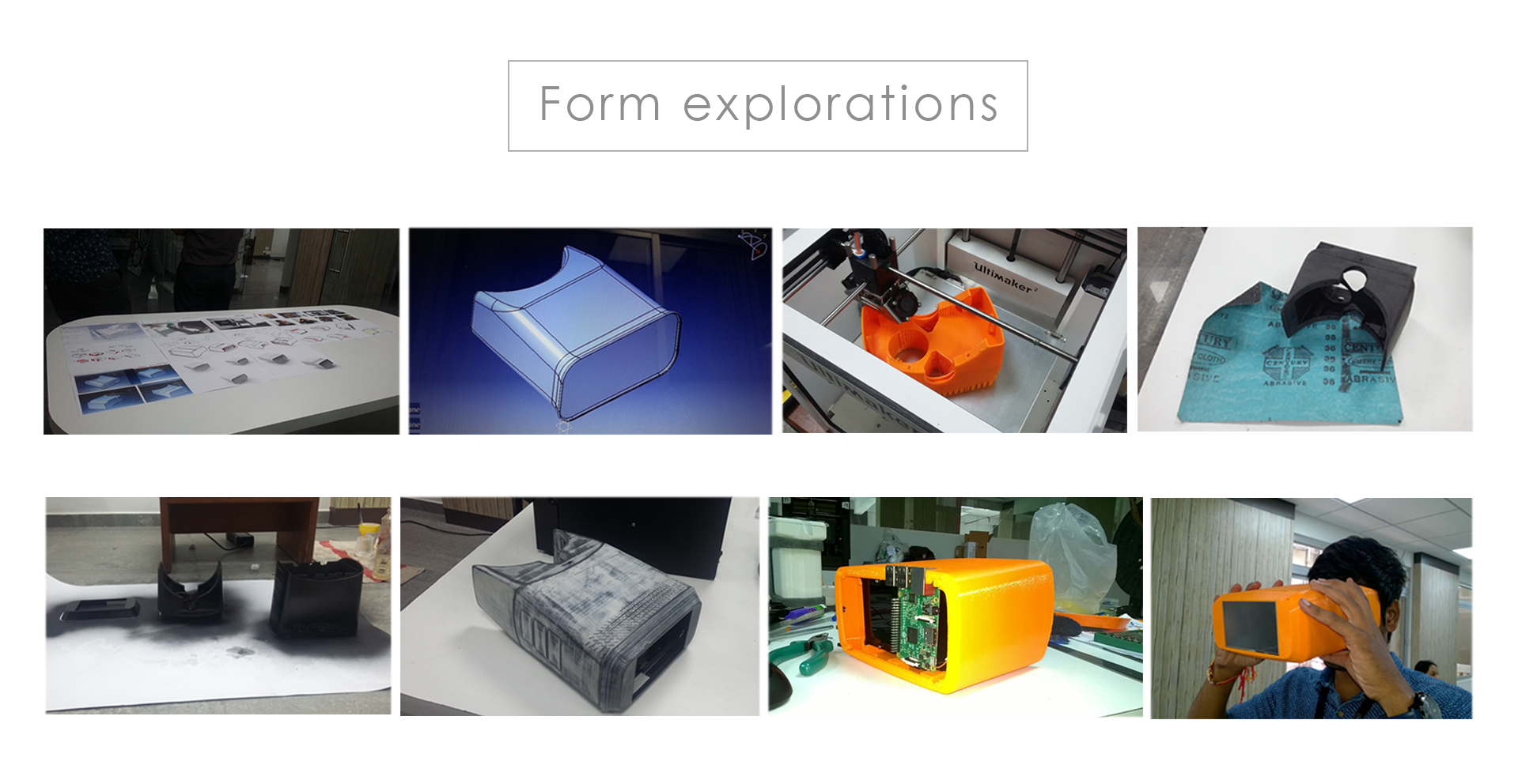
Several mock prototypes were tried and tested to get this particular ergonomic shape.
Also the protruding end at the temples ensure a further assurance of a perfect fit.
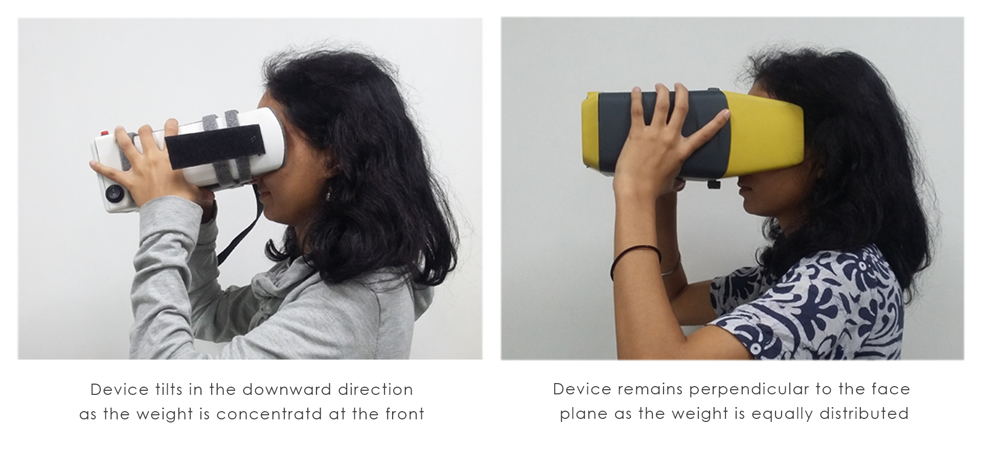
4. WEIGHT DISTRIBUTION
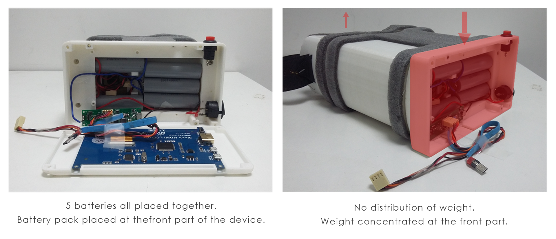
The earlier prototype had the battery bank at the front of the device.
Hence, the device tended to sag(hence it was not perpendicular to the face plane)
BEFORE
![]()
AFTER
![]()
The batteries have been re-distributed at the middle portion of the device to reduce weight at the front end.
As a result, the sagging reduced and the device stayed perpendicular to the face plane.
![]()
-
Optimization of Electronic Components
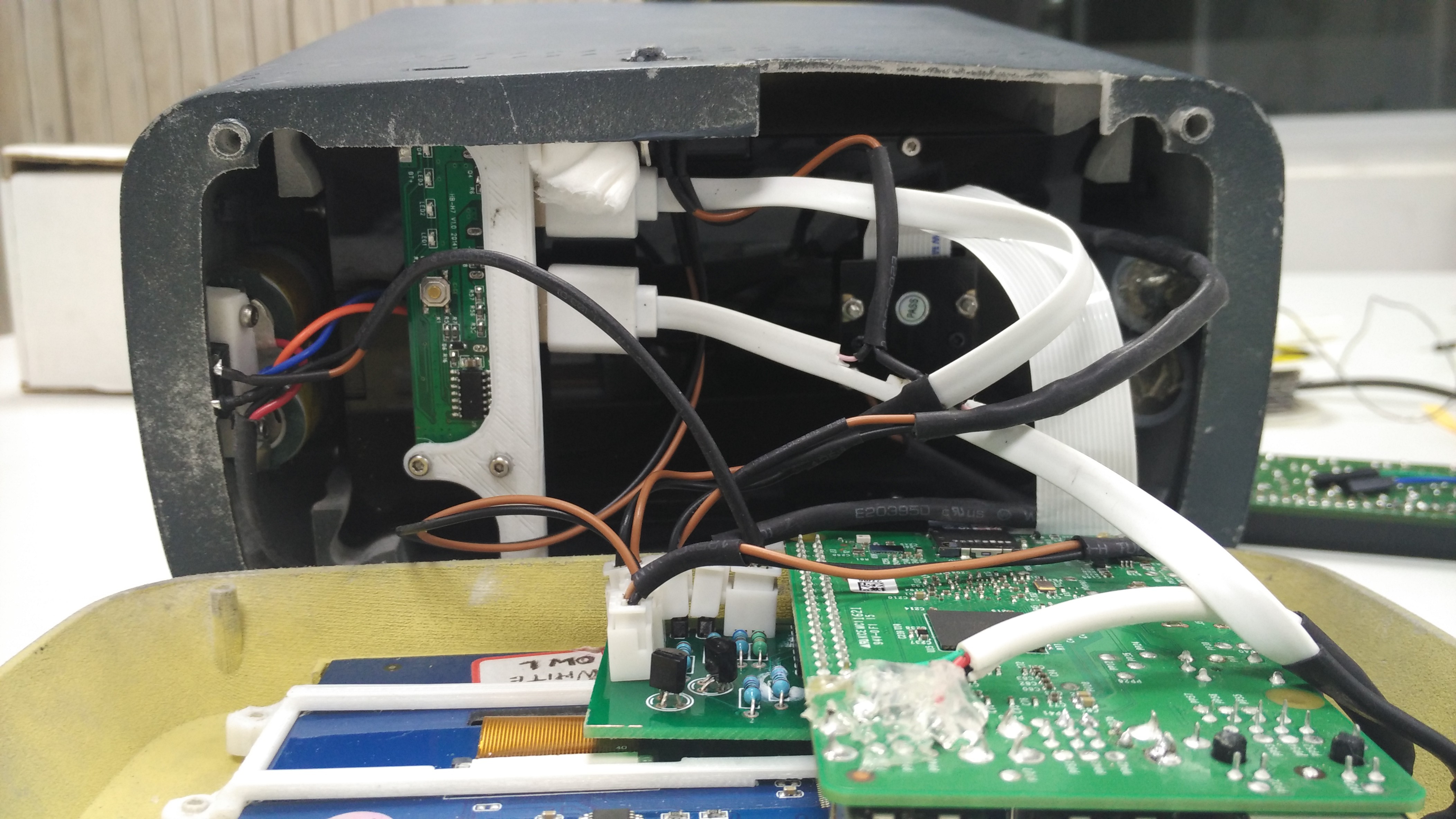
10/06/2016 at 08:46 • 0 commentsThe messy wires inside the device can be taken care by decreasing the lengths of the wires. All the connectors should be standardized so they can be easily reproducible.
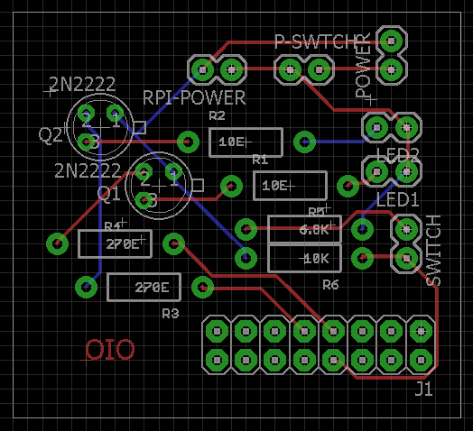
We can start with the PCB. The earlier PCB was used for prototyping. It has 8 slots for the multiple LED's for testing to get the proper illumination on the Retina. Now we know, we only need single LED to shine the Retina. So the extra slots can be removed and the PCB can be compressed.
![]()
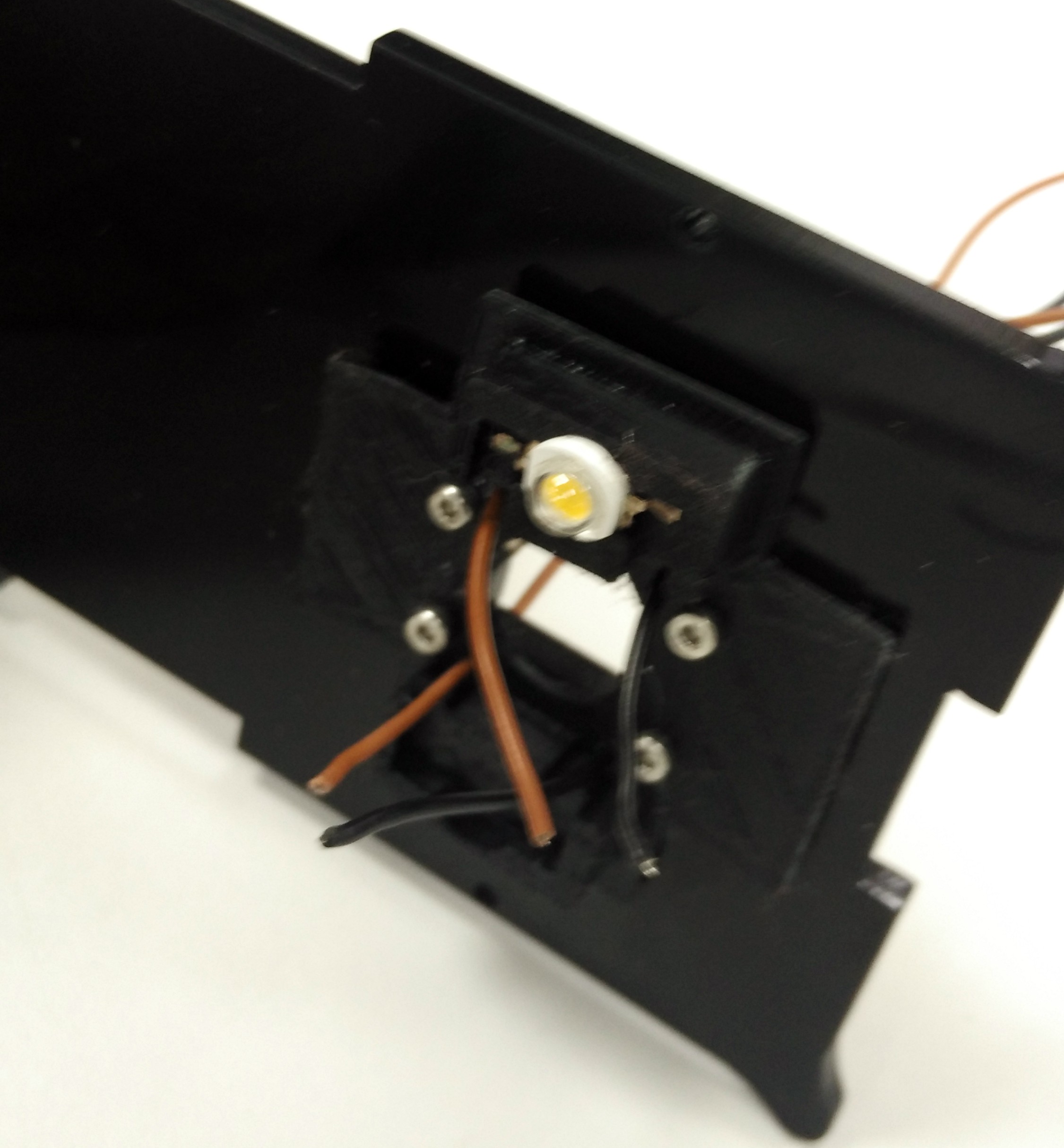
LED Placement
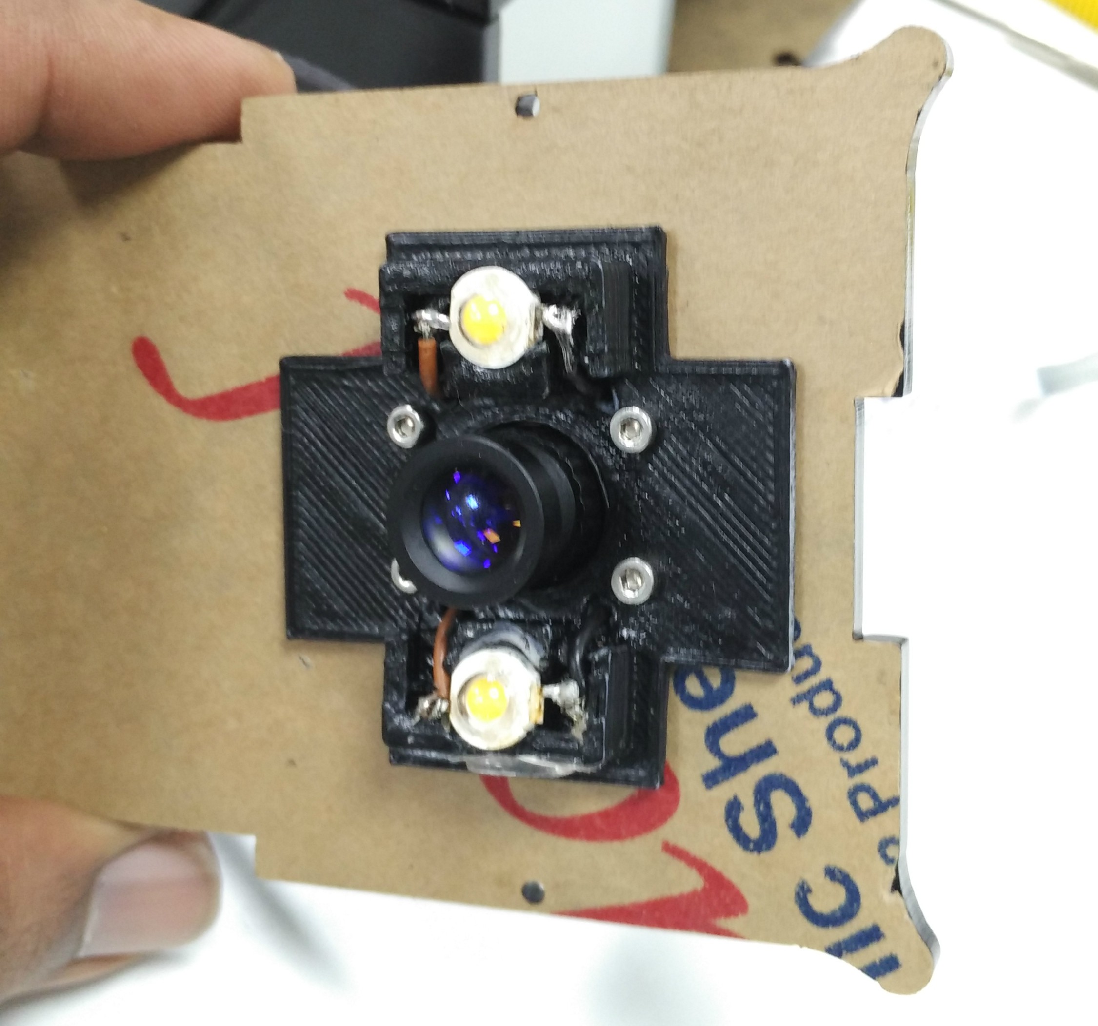
If you see the LED, it is placed on the top of the camera by which we are capturing the image of the left eye's Retina. If we need to get the same standard image on the right eye as well, then we need to place a LED on the bottom so that when the device flipped it comes on the top of the camera. Thus we can get standard images from both eyes.
![]()
TWO LED's
So a new PCB with only 2 LED ports can be made.
PCB Design
PCB Assembly
![]()
Touch cable on R-Pi
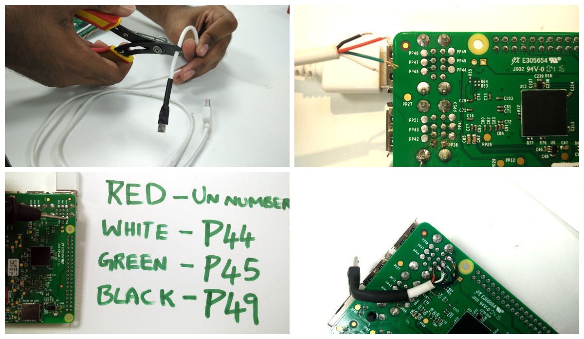
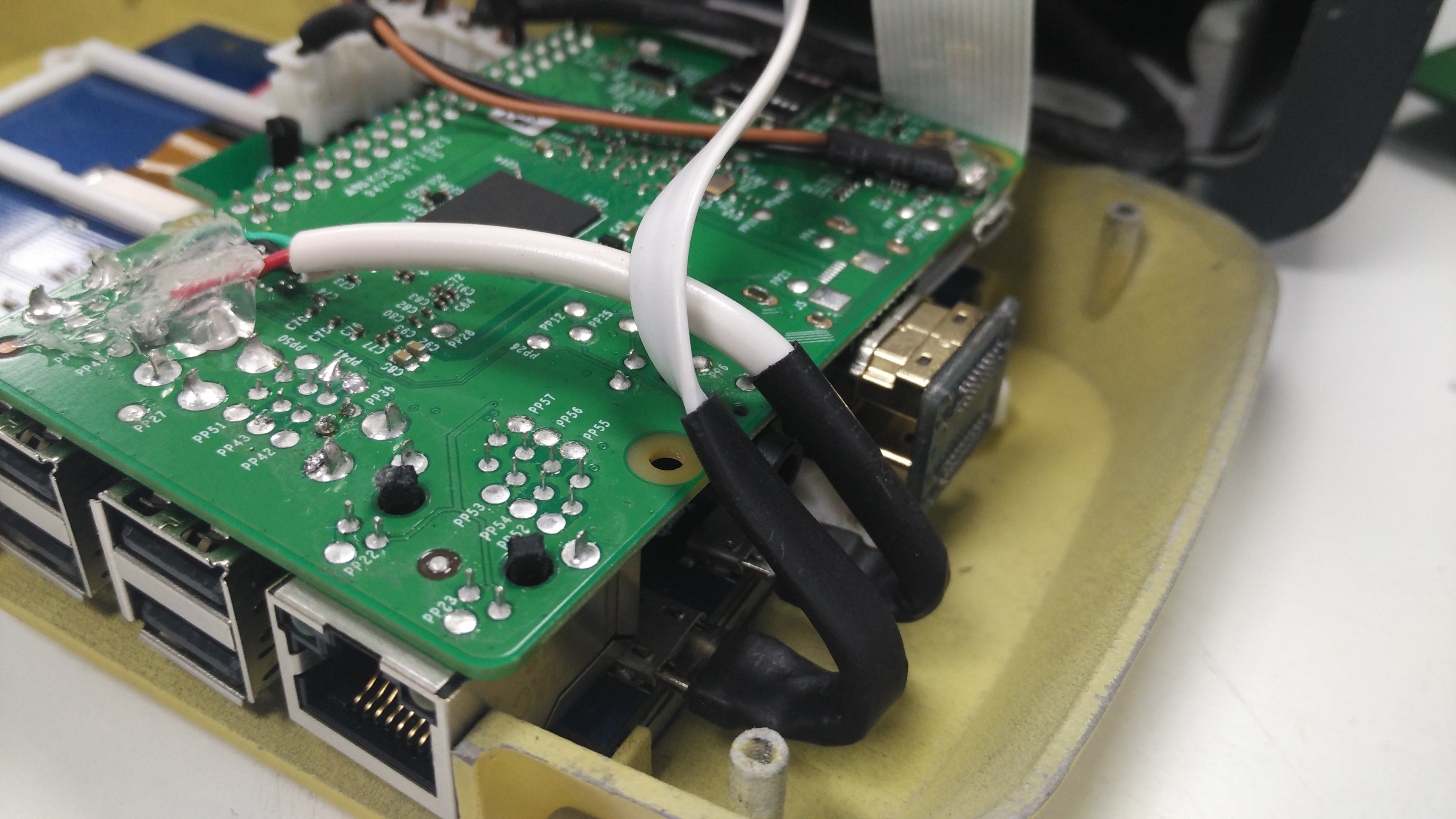
The cable for touch from one of the R-Pi USB ports to the screen can be by passed. By finding the corresponding solder connections for a USB port on the R-Pi we can solder the USB cable's wires directly to those points and decrease the length of the wire.
![]()
Power Input for R-Pi
The micro USB power input to the R-Pi can be by passed by soldering two terminals to the +/- on the R-Pi and connect them on the PCB
![]()
Power Cables from Power Bank
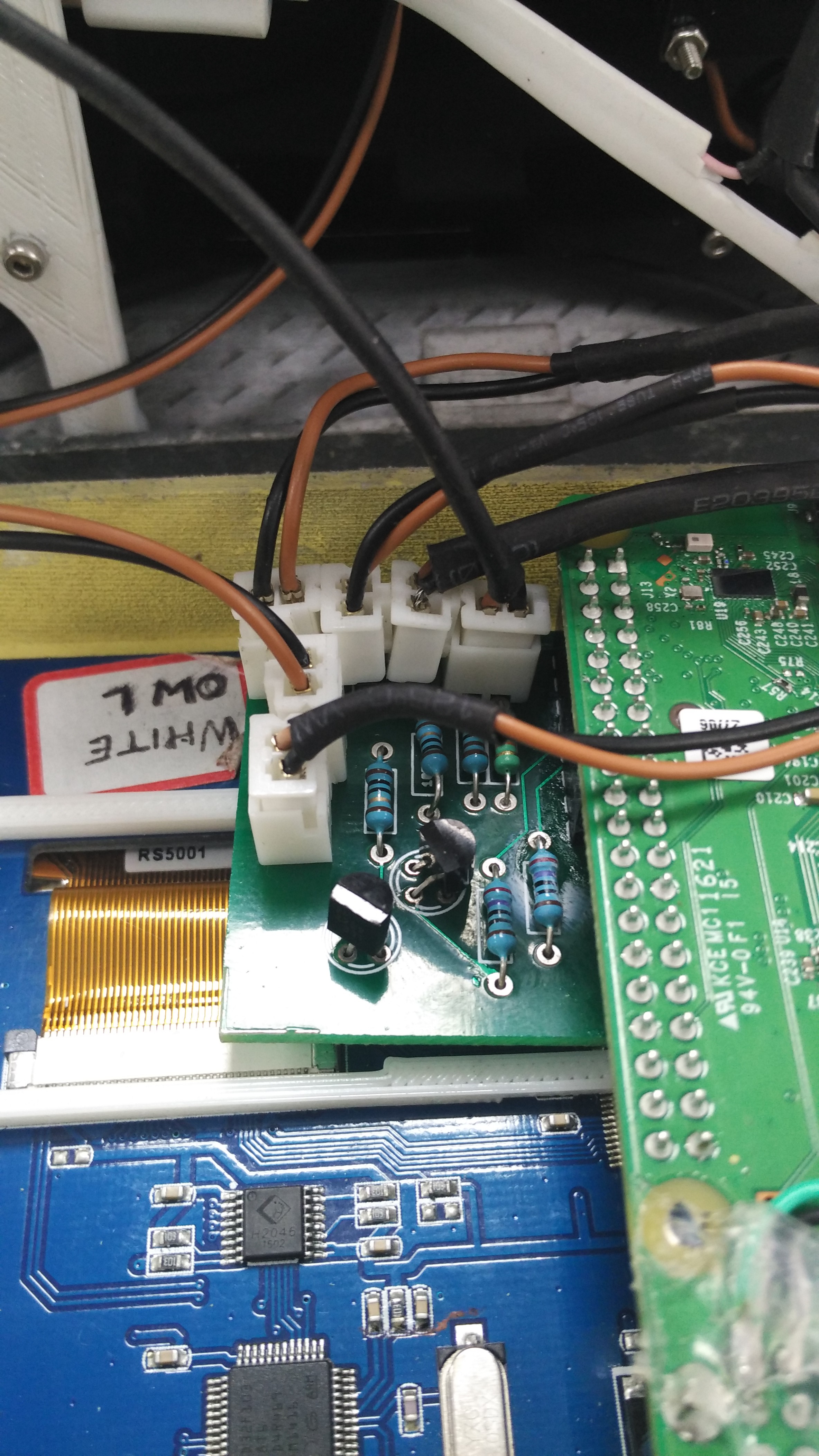
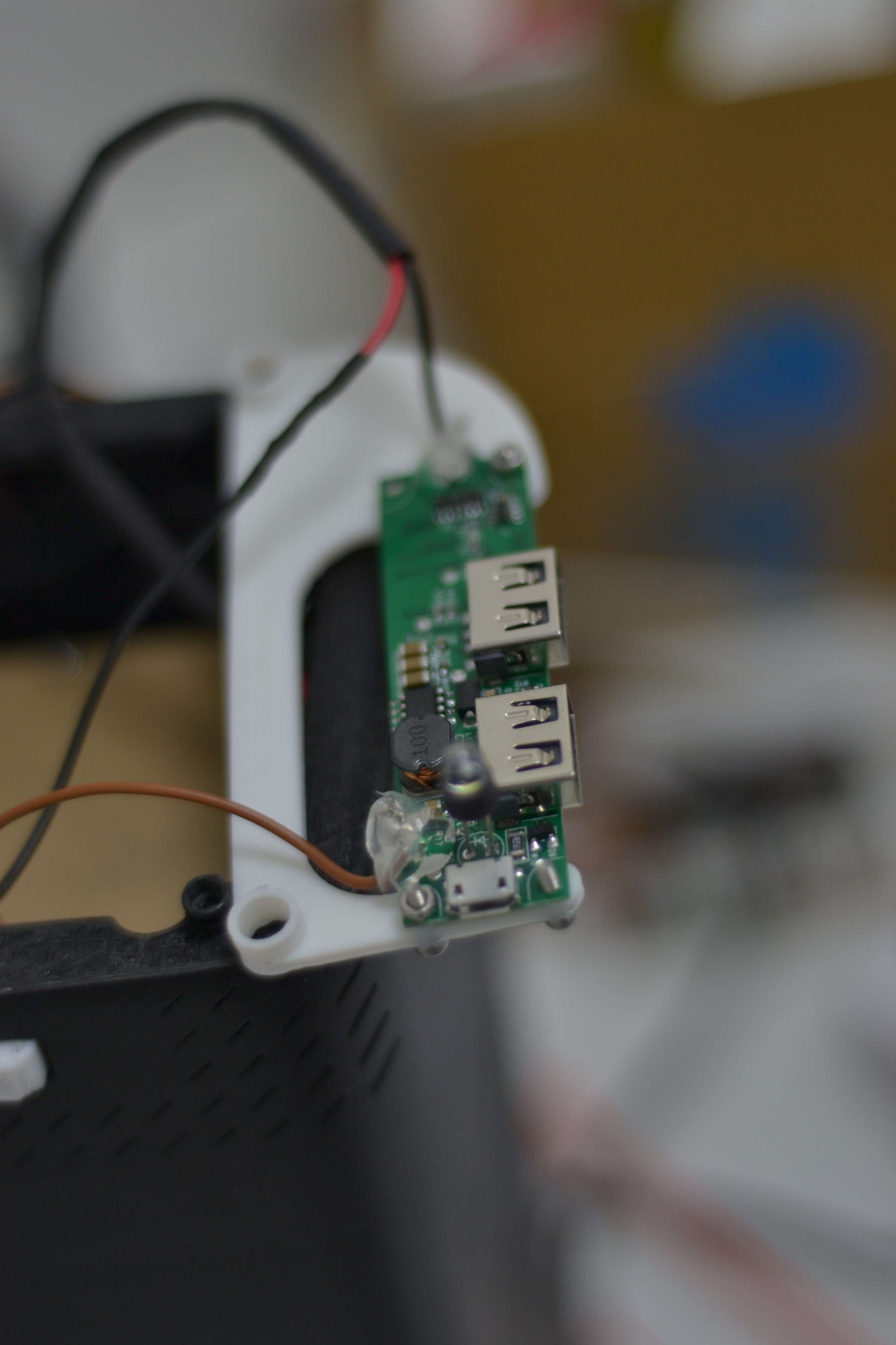
Power bank has 2 USB female ports. One is 2.0A and another 1.0A. The PCB need to drive the R-Pi and the LED's so 2.0A can be directed to PCB. Instead of desoldering the USB ports on the power bank PCB connect a 2 pin female connector to a USB cable (Soldering micro USB female to the PCB is time taking). This will connect the power bank PCB through USB and to the main PCB it acts as a power input terminal with a 2 pin connector.
![]()
LCD screen couldn't take sufficient power from the touch port. As a result the touch malfunctions once R-Pi starts accessing the camera. So we need another power source so that's why we are using the 1.0A for the Screen.
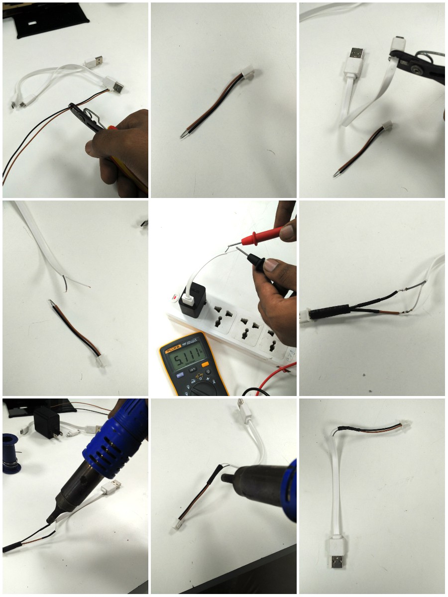
R-Pi and screen works on the same power source which is always on. For the R-Pi a switch slot is already given. Now the screen works on an independent power source which should be connected to a switch. So we need to add another switch to the screen power cord (Can add a 5V relay but it drains the power bank). Slit the cable and add a slide switch any one of the terminals.
The end of the cable is micro USB which is covered by a thick plastic layer. Because of this the cable can't bend and fit into the enclosure of front piece. So chip off the plastic with a knife and insulate it with a heat shrink.
![]()
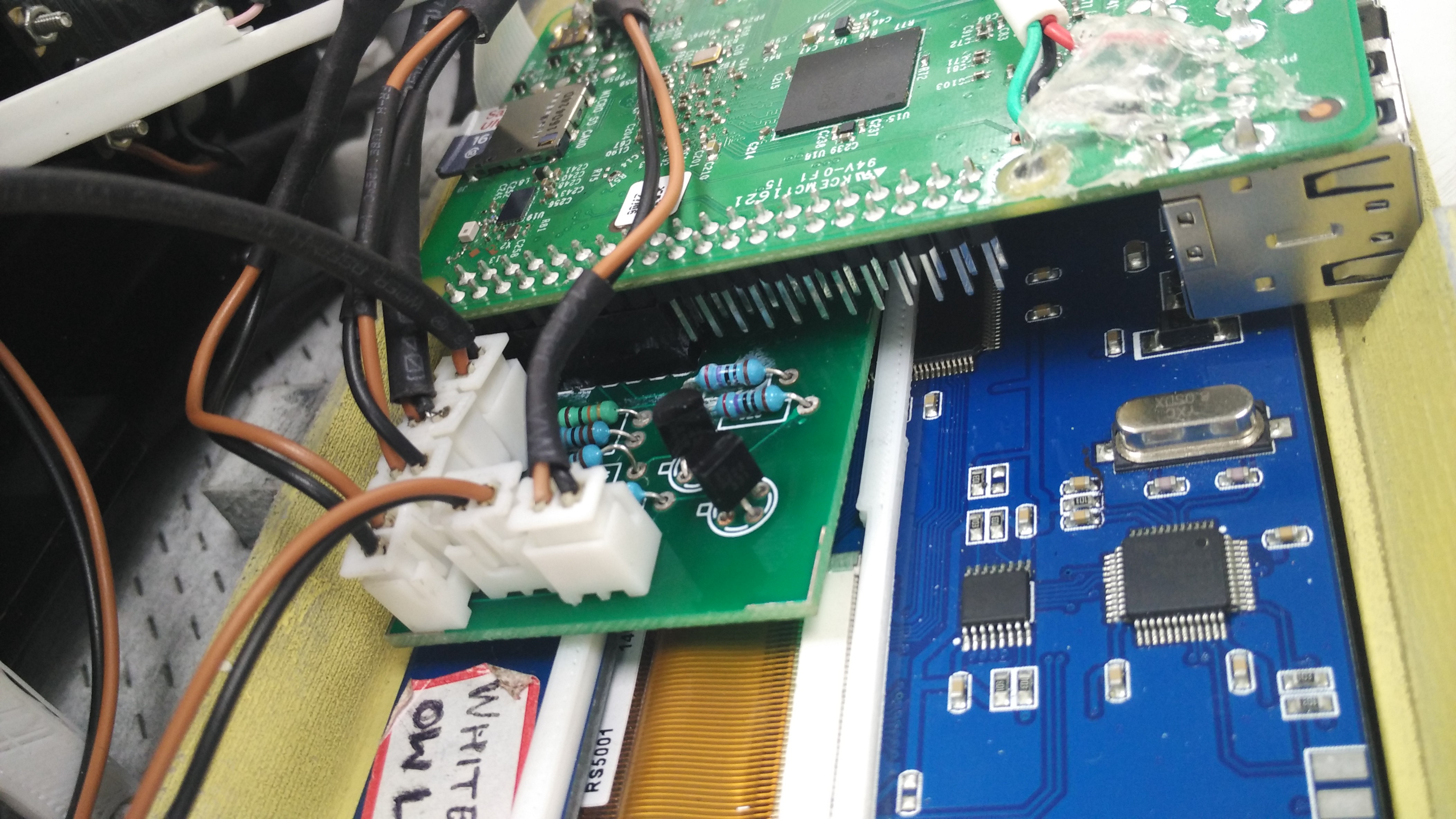
Connectors Standardization
![]()
OUTPUT
![]()
![]()
![]()
-
Multiple Minor Software Tweaks
10/04/2016 at 04:31 • 0 commentsA number of minor tweaks were done to the software to make sure that the software runs smoothly.
Individual tweaks can be viewed from the GITHUB repo.
Here we'll mention about the two major updates that were done which may not be visible normally.
1) Changing of the pins : The GPIO pins have been changed for the LEDs . This is because the printed PCB was fitting into the GPIO only in that manner.
Although there was no major update in the code that was there but the pins are now changed and it can be something hard to find.
2) Allowing multi-threading in the flask app : The flask app was crashing every now and then whenever we wanted to get the theia grading. This was later solved using the following attribute while running the app.app.run(host='0.0.0.0', threaded = True)Earlier it was giving an 'Internal Server Error' if Theia returned no value or timed out.
Next up is creating a robust system for handling all types of errors. -
Design Changes: Internal Assembly
09/22/2016 at 12:26 • 0 commentsOptic Box:
For making the device screen people with different refractive error the optic box had to be moved inside the casing. To achieve this, a sliding system was created by making positive rails on the optic box and negative rails inside the casing.
Optic Box
The box has stress at the edges as its weight is concentrated at the rails. Hence the strength of the edges of box had to be increased. Holes at the edges were provided for mounting screw fasteners to increase the strength of the optic box.
Sliding System with Rails
Rack and Pinion Mechanism:
To impart motion to optic box, rack and pinion mechanism has been used. The rack has been placed on the optic box and the pinions are assembled inside the eye piece with a rod which transmits motion to different planes and eventually to the racks. The pinions are assembled inside the eyepiece with the help of a bracket. The bracket holds the pinion in its place while giving it freedom to rotate in the plane.
Rack and Pinion Assembly
LCD:
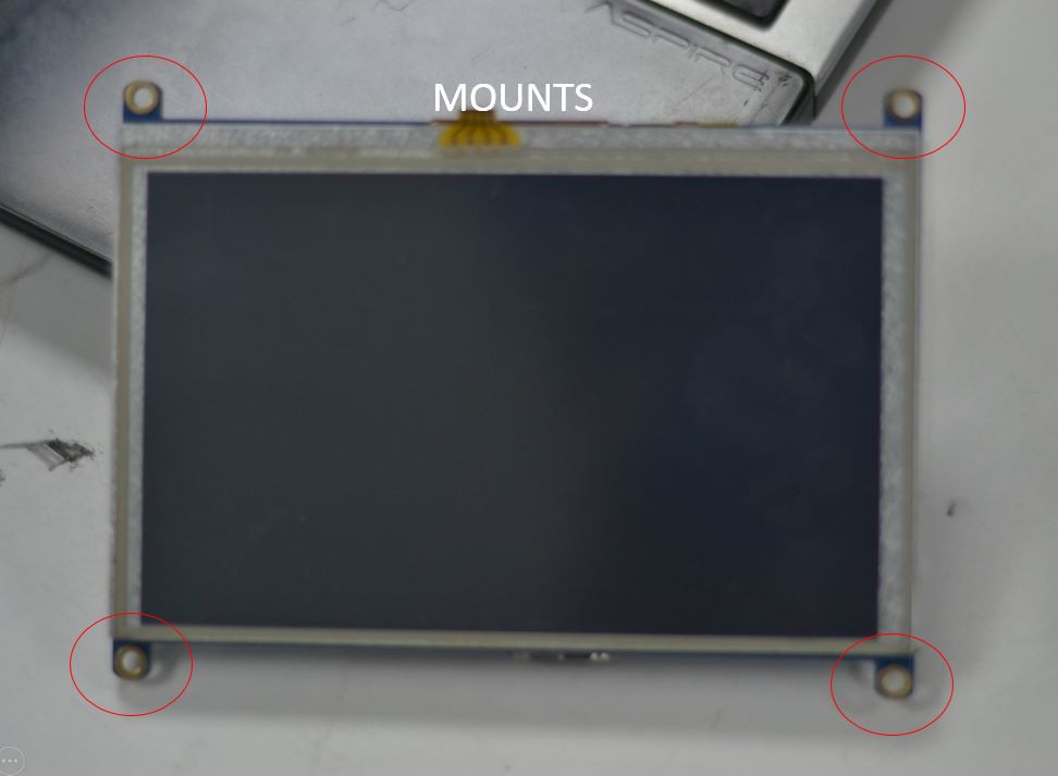
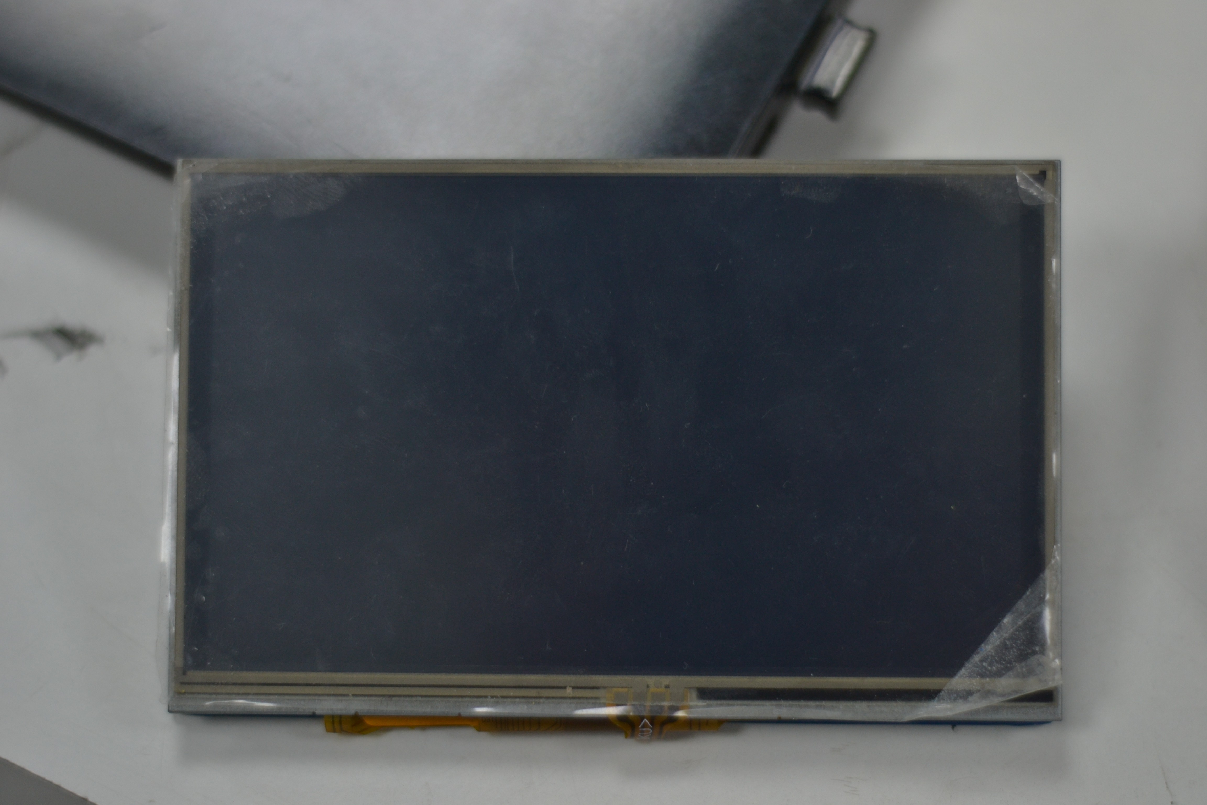
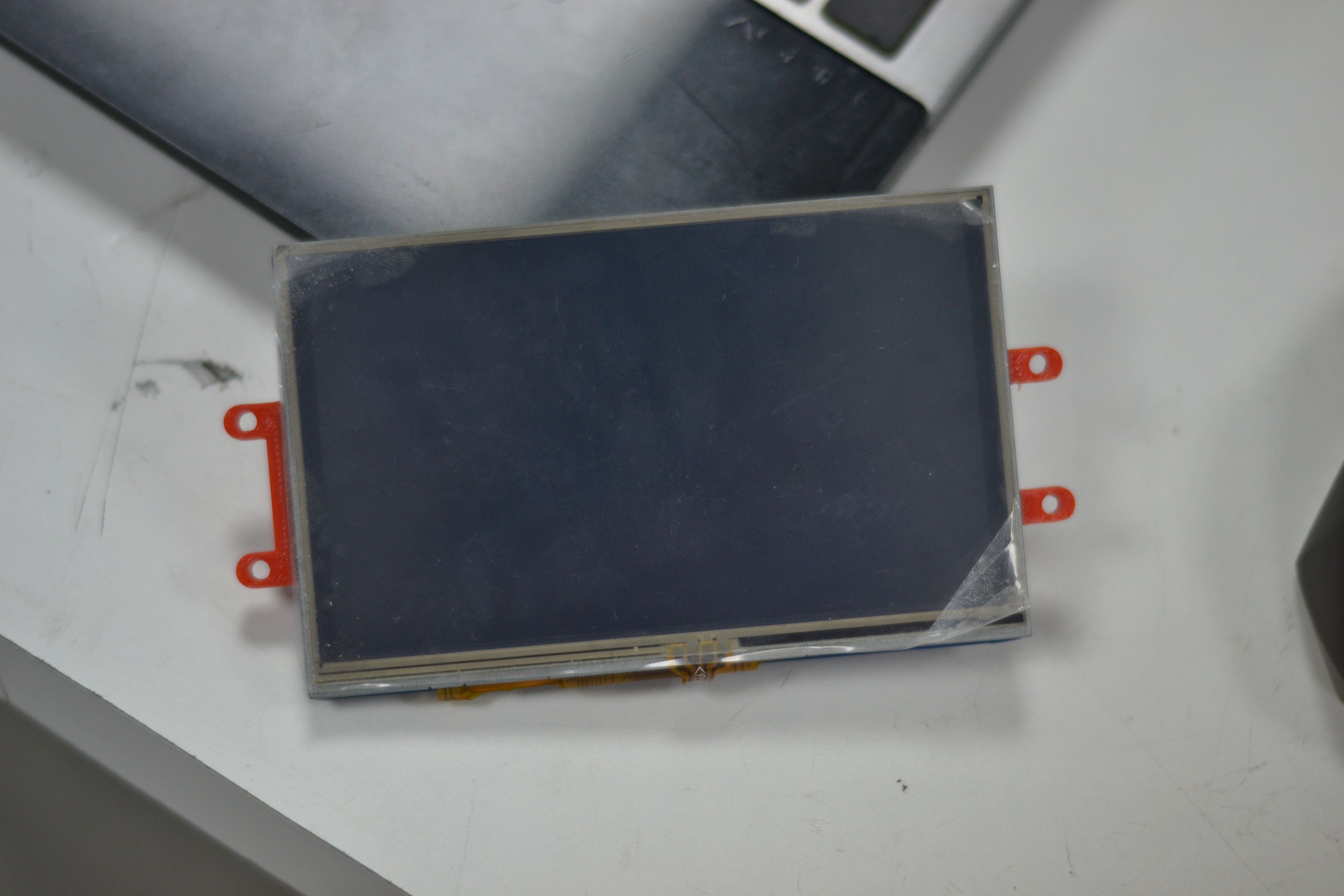
The Waveshare 5 inch LCD has mounts to assemble the LCD onto a surface using screw fasteners.
LCD with mounts
But, to accommodate the LCD inside the front casing we have to cut the mounts that come with the LCD.
LCD without the mounts
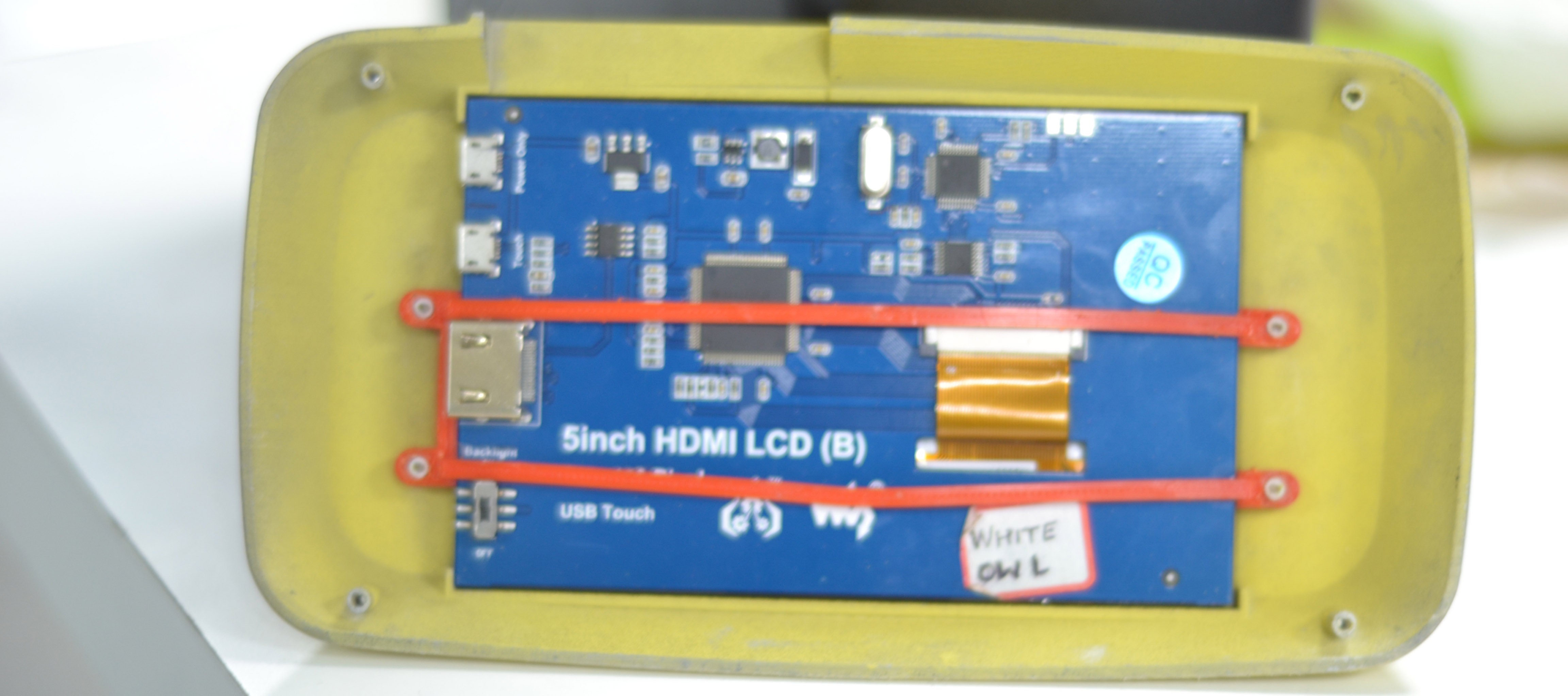
To assemble the LCD with the Front casing we made a support for the LCD which would act like a mount for the LCD.
LCD with printed support
![]()
LCD Assembled inside the middle casing
![]()
PCB of Batteries:
The PCB of the Batteries has to be placed inside the Middle casing. To assemble it inside the middle casing a mount has been created on which the PCB is fastened with the help of nut and bolt fasteners.
Batteries with the PCB
PCB with the mount
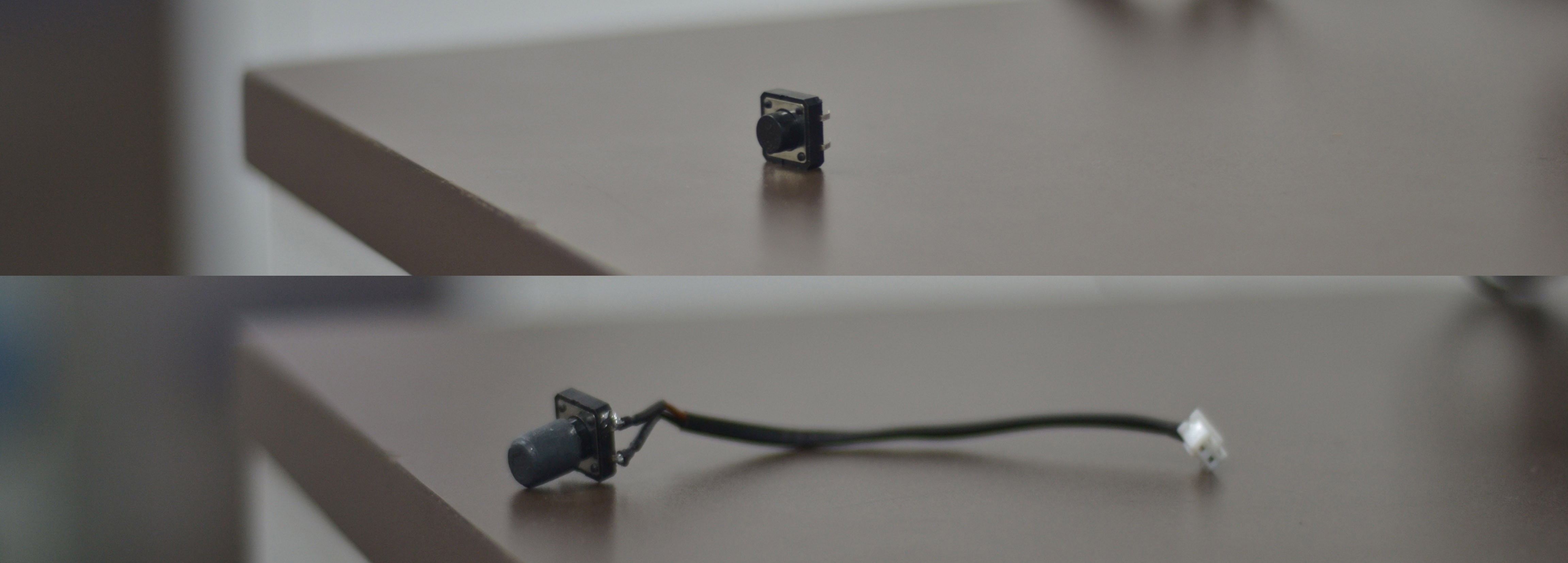
Click Switch:
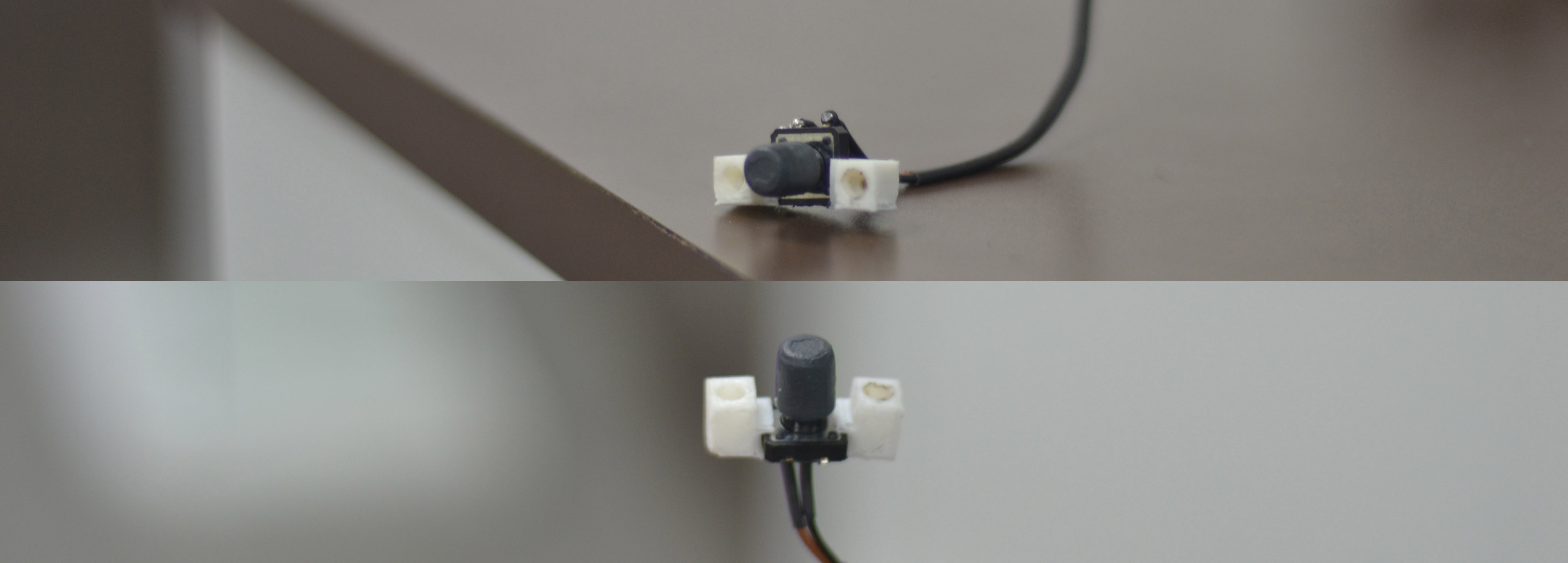
The Click switch has been mounted inside the middle casing using a mount. It is first mounted into the mount and is then assembled inside the middle casing using screws.
![]()
Mount for Click Switch
![]() Click Switch
Click Switch
![]()
Click Switch with mount
![]() Click Switch Assembled inside the middle casing
Click Switch Assembled inside the middle casing
![]()
Knob:
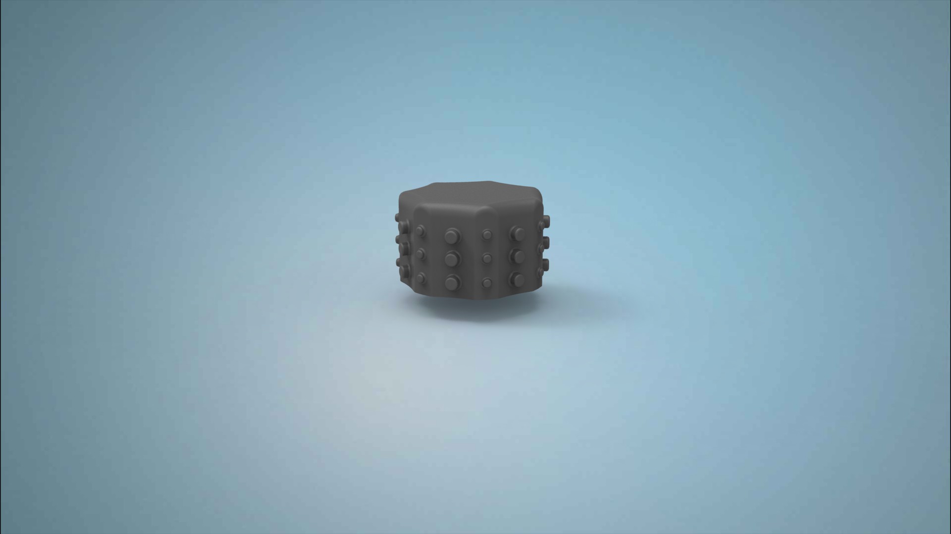
The knob made earlier was slippery, thus the total motion imparted was not transmitted due to slipping. The knob is given texture to increase grip and friction and help in transmitting motion to the rod.
![]()
Textured Knob
Toggle Switch:
To regualte power to raspberry pi and LED's, a switch has been incorporated in the pcb. But there wasn't any switch to on/off the LCD screen. Thus a double switch was made which would facilitate as a switch to both the screen and raspberry pi,LED.Here are some of the images showing the making of a double switch.
![]()
The Cable with a switch
![]()
Double Switch
![]()
Double Switch inside the Middle casing
Camera Spacer:
To mount the camera to the Optic box a 4mm mount is used to create space between the optic box and the camera. This is needed to ensure that the camera is perfectly centered and parallel to the plane of sight.
![]()
Spacer
![]()
Camera without spacer
Camera with spacer![]()
![]()
Assembly of Spacer with camera and Optic box
-
Electronics - Power Bank & Custom PCB
09/16/2016 at 06:16 • 0 commentsThis log talks on how to assemble the internal circuits of Open Indirect Ophthalmoscope.
Dismantling:
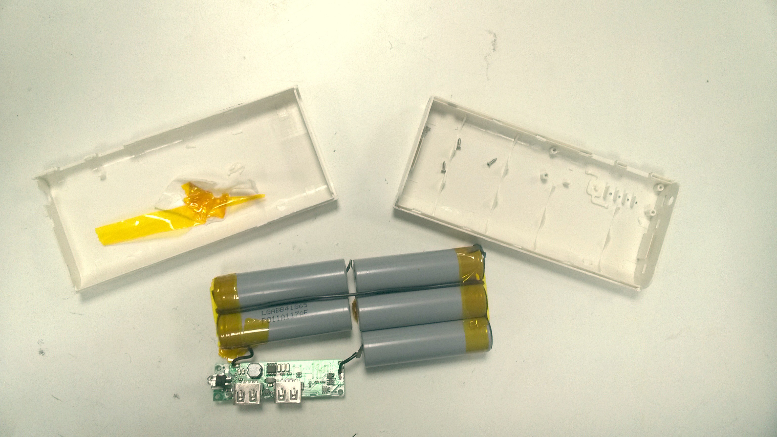
Crack open the power bank (13,000 mAh power bank with power output of DC 5V, a device with two output USB ports such that one gives a current of 2.1 Amps and the other 1 Amp.)
The reason for choosing a power bank with two such outputs is that the LED circuit and the RasPi together need a higher current, which in this case is being powered by the 2.1 Amp port and the display is powered by the 1 Amp port.
While doing this, care should be taken that the circuit is not damaged. Power cables are soldered onto the PCB, therefore after cracking, do not jerk open the bank.
Here are some references for the power banks that can be used.
http://amzn.to/2cNw0av
http://amzn.to/2d4wjNt
It is preferable to use a power bank with the USB A Type and Power Bank Charger - USB B Type on adjacent sides. This makes the assembly easier.Remove the batteries carefully from the casing. There should be five batteries, remove one battery out from the circuit by cutting the metal plate interconnecting the batteries.
![]()
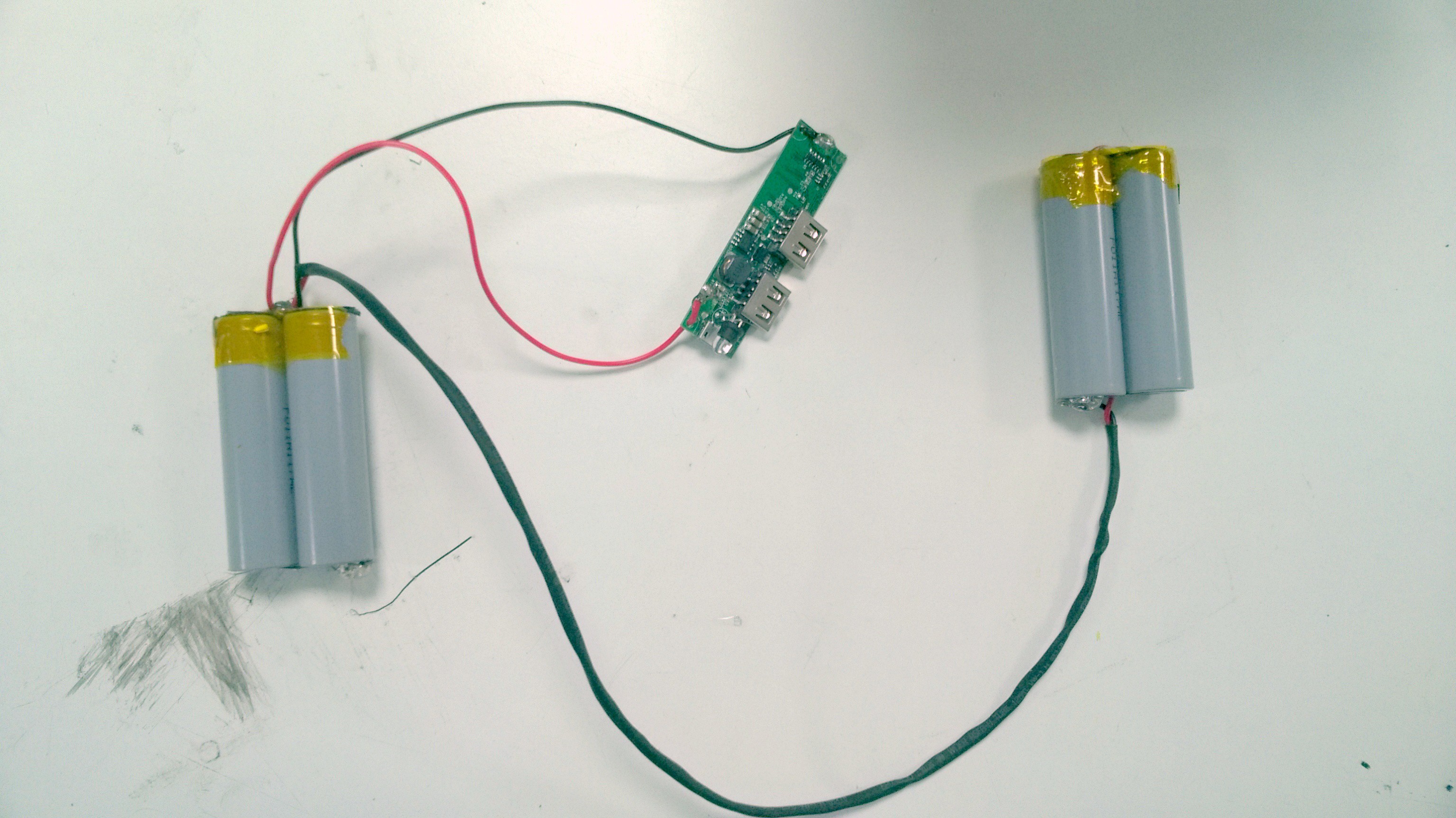
Once this has been done, separate out the batteries into sets of two with both sets electrically parallel to each other. At this point connect two sets of wires connecting two sets of batteries, while doing so place the heat shrink material in the wire, this will be used to make the wires appear seamless and give them strength once all the connections have been soldered.
![]()
The separation of batteries is done so as to provide an even weight distribution throughout the chassis. Placing two sets of two batteries each makes the weight balance out horizontally.
These wires should be placed such that the ones connecting the positive ends are slightly longer than the negative ones. Carefully pass the positive wire in the crevice between the batteries. Solder the negative terminals. The resultant battery setup should look like this:
This allows the batteries and the wires to seamlessly fit in the battery encapsulation groove in the 3D printed assembly. Carefully place the batteries and check the wire lengths.
Now take the PCB from the power bank and increase the length of the wires connecting the batteries to the PCB. They should be connected onto a terminal 'B+' for the positive terminal and 'B-' for the negative terminal respectively. Solder the terminals and seal the solder with silicone glue to give the entire joint some strength.
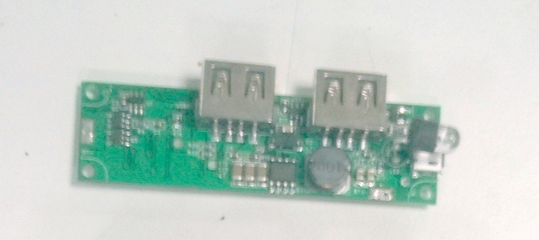
On the same PCB extract the USB ports by heating their soldered ends (4 Connections) from one side using a hot air blow gun or a solder gun and pulling from the other end simultaneously. Be careful to not pull too hard, as this might cause the circuit to get damaged.
![]()
After the USBs have been extracted, it's time to solder the cables connecting the power supplies to the PCB and the LCD.
Take a micro USB cable and cut off the non micro USB end. Strip this end and peel the wires out. There should be two wires (if you are using a charging cable) or four wires (if you are using a charging & data transfer cable). The standard colour combination is Red - for the positive connection and Black - for the negative connection. Solder the red wire to the positive end and black to the negative/ground on the power bank PCB at the 1 Ampere port. This cable will supply power to the custom LCD.
Take another set of two wires (red & black preferably) and solder the red end to positive and black end to negative/ground of the Power Bank PCB's 2.1 Ampere port. Take the other end of the wire and attach two female headers on to it. These will be connected to the custom PCB's power supply. This will be used to supply the power to the LEDs illuminating the retina and to the Raspberry Pi.
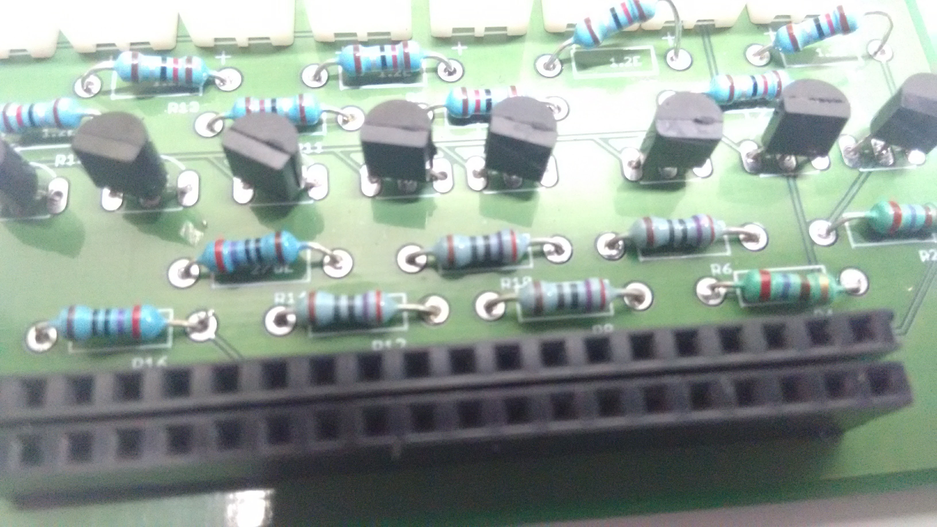
Soldering the Ras-Pi Shield PCB
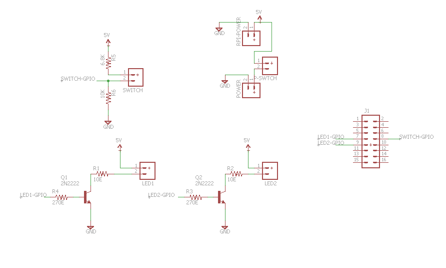
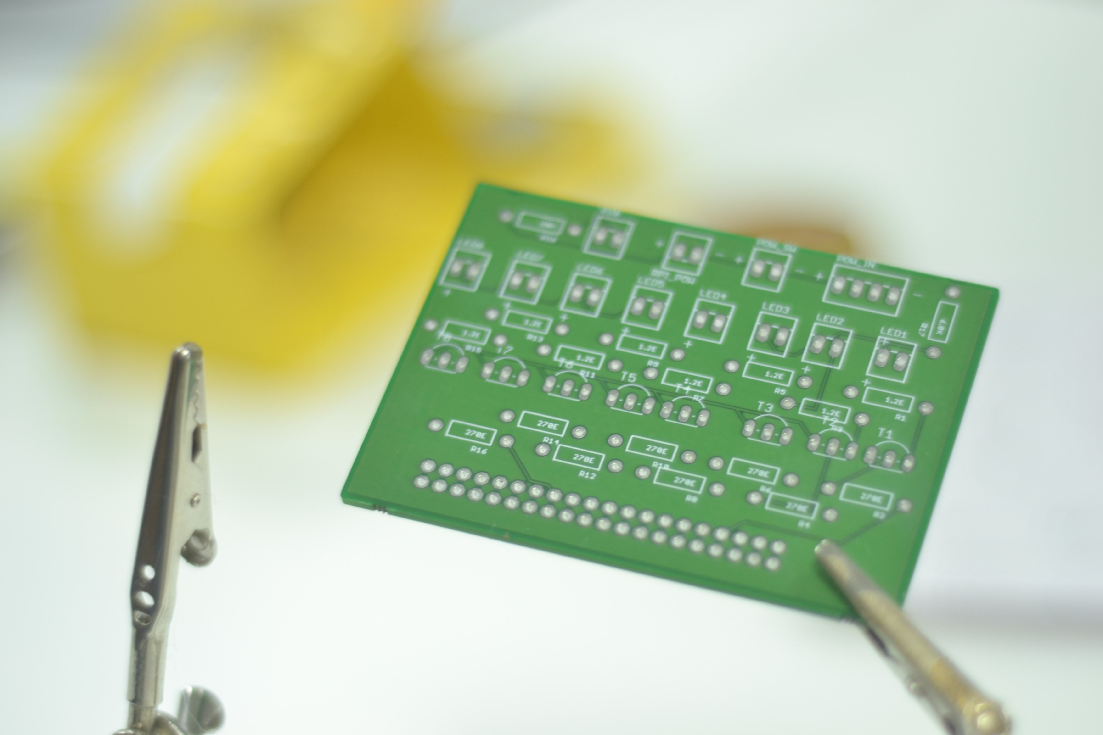
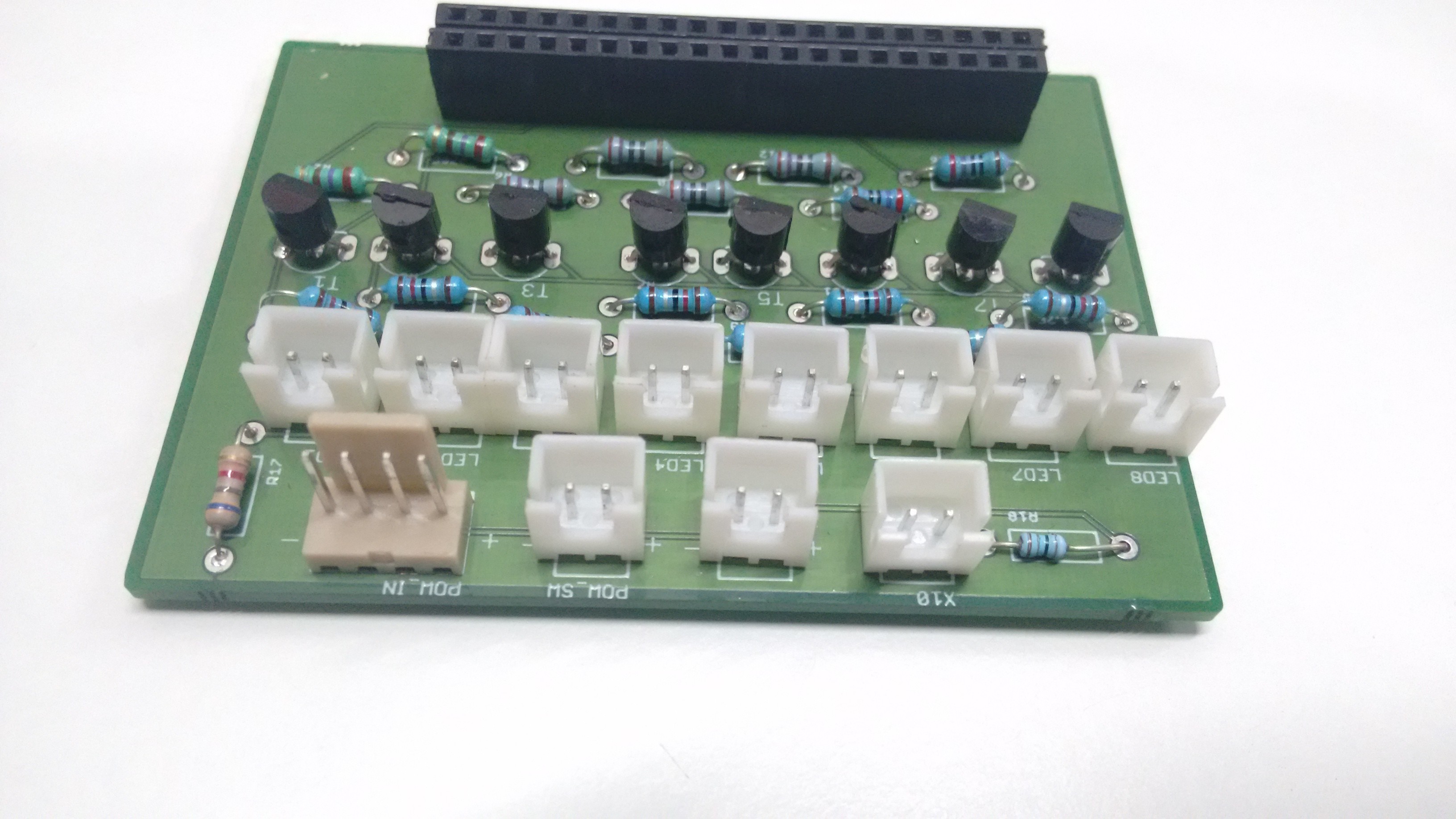
Place the 2N222 Bipolar Junction Transistors (BJTs) carefully on the PCB. Most PCBs come with a hemispherical marking and a flat end marking to ensure correct orientation. Though this may not be true in all cases, in such a situation one way to understand the placement is to place the transistor such that the flat side if facing you and the pins are pointing upwards, in the orientation the pins are in the order - Emitter-Base-Collector from left to right (clockwise order). The connections of emitter base and collector are as follows with standard notations applicable.
![]()
For any other clarifications please refer to the Schematic and Gerber files.
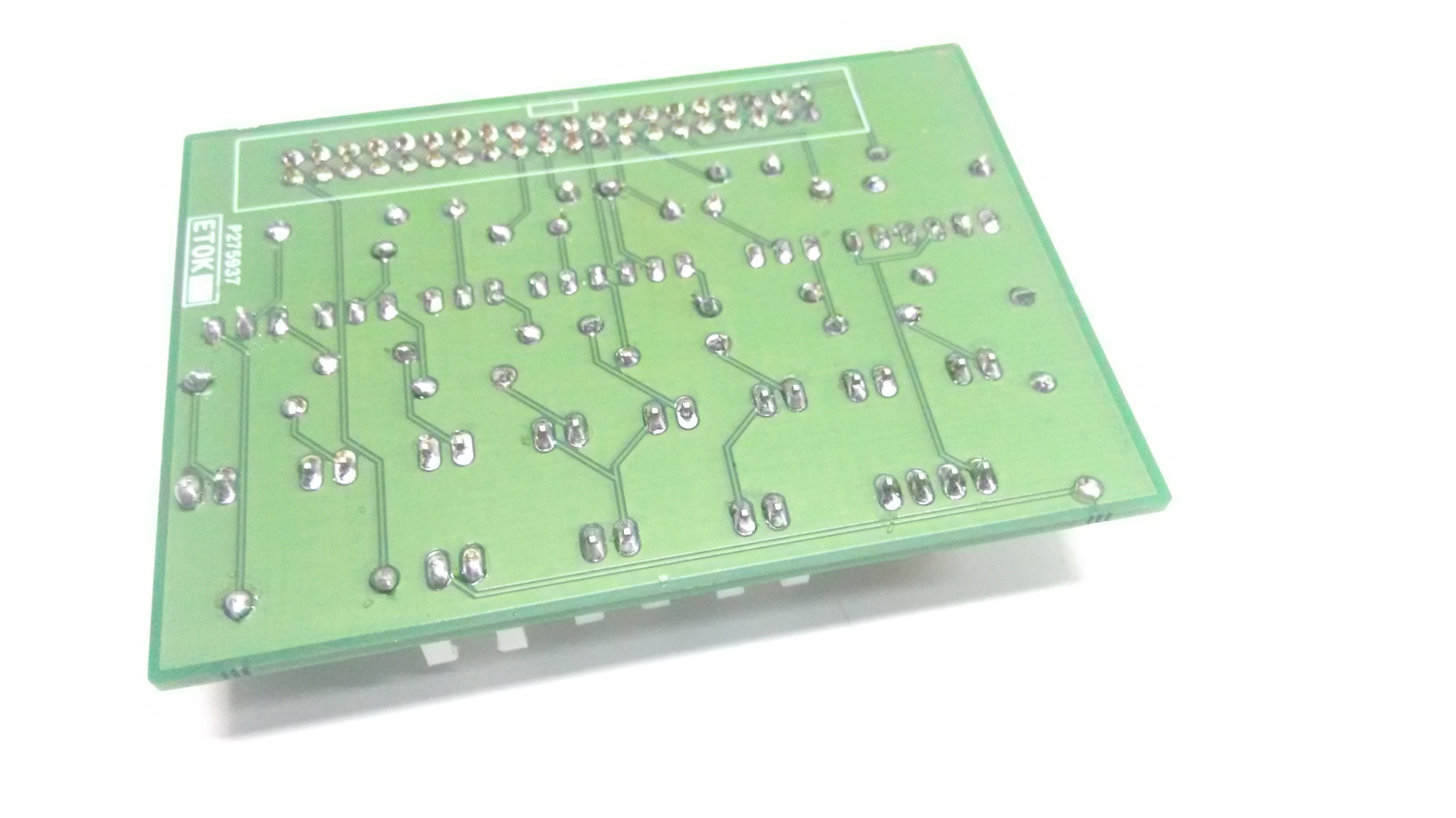
Place the female headers on the rail that falls directly on to the Raspberry Pi GPIO Pins. Remember the pins of the RasPi are male headers. Once this is done, solder each node separately and carefully. Ensure that there is no extra solder blob.
Now carefully take 8 resistors each of 270 Ohms (Colour Code: Red | Violet | Brown | Gold) and place them below the transistor on the ports marked as | 270E |. Solder each carefully and cut off the extra metal from the terminal.
Again take 8 resistors each of 12 Ohms ( Colour Code: Brown | Red | Black | Gold ) and place them at the ports above the transistors, marked as | 1.2E |. Solder each carefully and cut off the extra metal from the terminal.
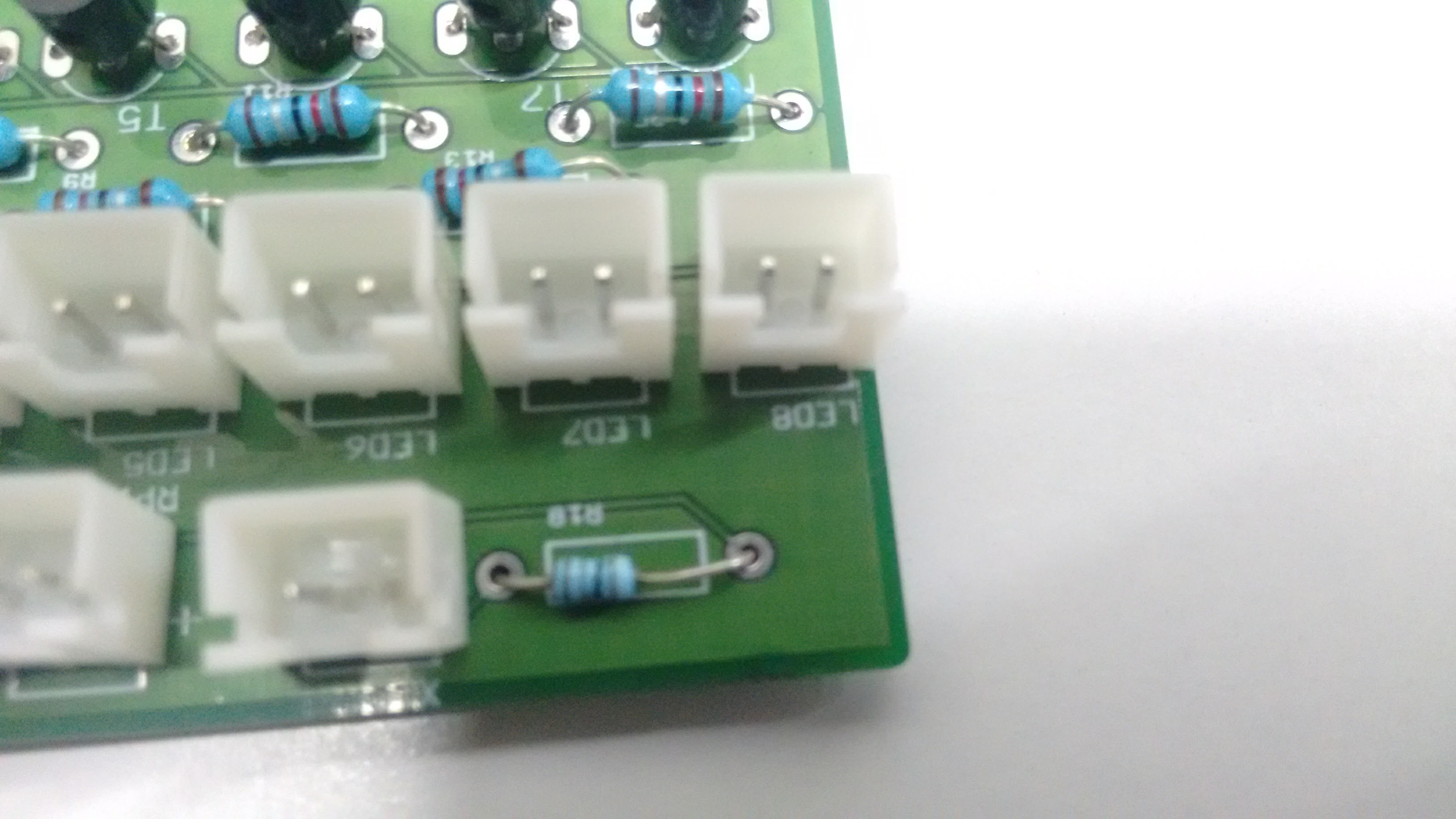
Take a 10K Ohm (Brown | Black | Orange | Gold) resistor and place on the top left slot for it labelled as R18. Solder and remove extra ends from the terminals.![]()
![]()
Take a 6.8K Ohm ( Blue | Grey | Red | Gold ) resistor and place on the top left slot for it labelled as R17. Solder and remove extra ends from the terminals.
![]() Now take 11 two-pin male headers and place them on the top of the PCB. Solder them carefully form the other side of the PCB.
Now take 11 two-pin male headers and place them on the top of the PCB. Solder them carefully form the other side of the PCB.Take a 4-pin male header and place it on the power port on the top right of the PCB, adjacent to the 6.8 K Ohm resistor and solder carefully.
The PCB should look like this once everything has been soldered.
![]()
![]()
-
Design changes
09/03/2016 at 10:53 • 0 commentsPain points in the present model and ideation for next prototype:
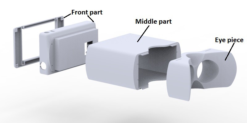
The earlier device housing was made in three part assembly which made it easy to assemble and disassemble during bugging. So the same method will be used in the coming prototype as well. The three parts are
- Eye piece (Through which the camera see's the eye)
- Middle part (This houses the optical setup with the camera)
- Front part (This contains screen, Rpi and PCB's)
![]()
Detailed description of pain points and ideation process.
The user interaction of the device:
- Eyepiece fitment on the examinee eye
![]()
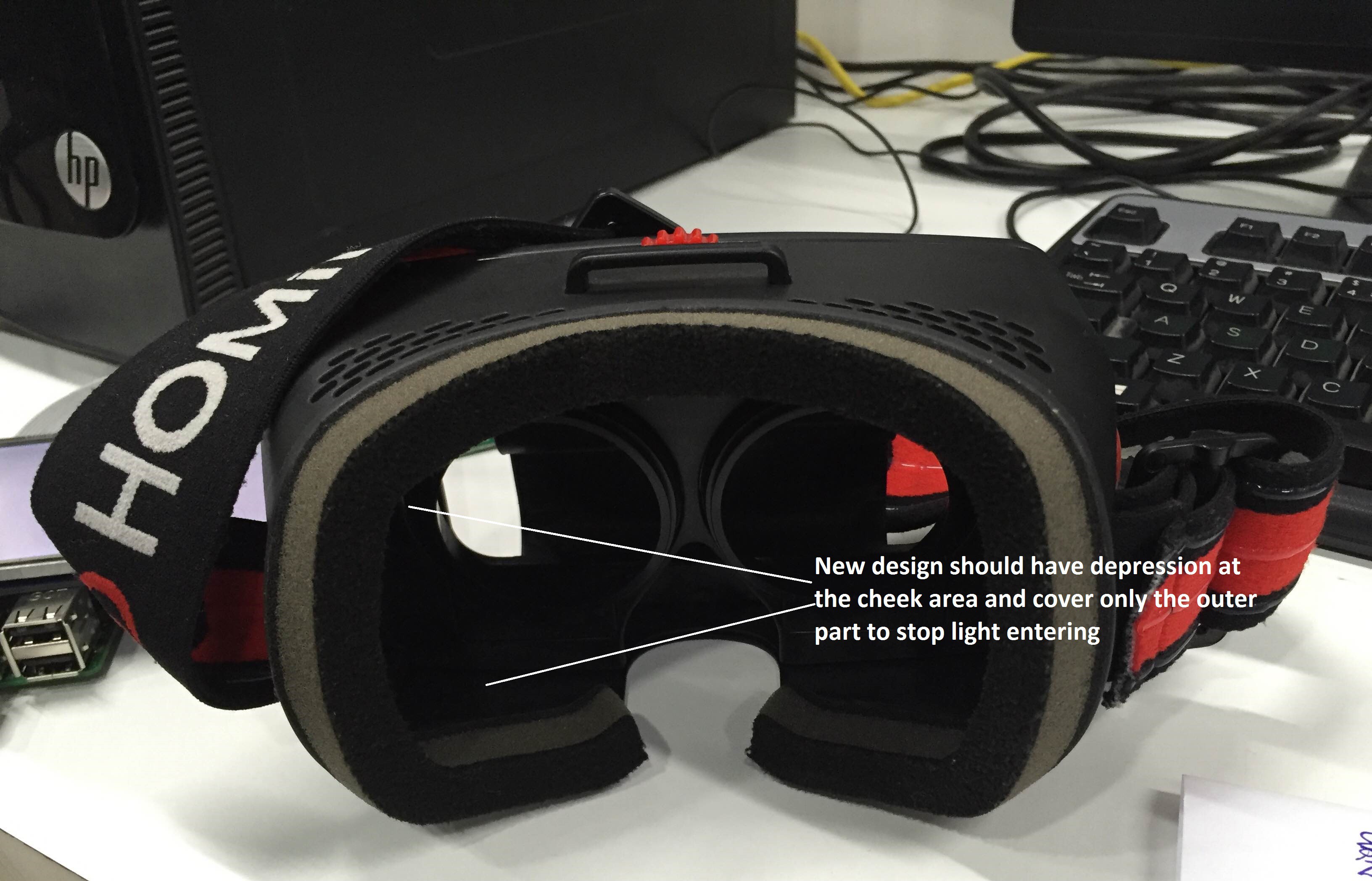
- The present model doesn't have proper grip to hold it. This caused slipping of the prototype while testing . Proper gripping has to be given to hold the device while testing.. This can be solved by giving embosses with ergonomic hand detailing on the middle part of the device.
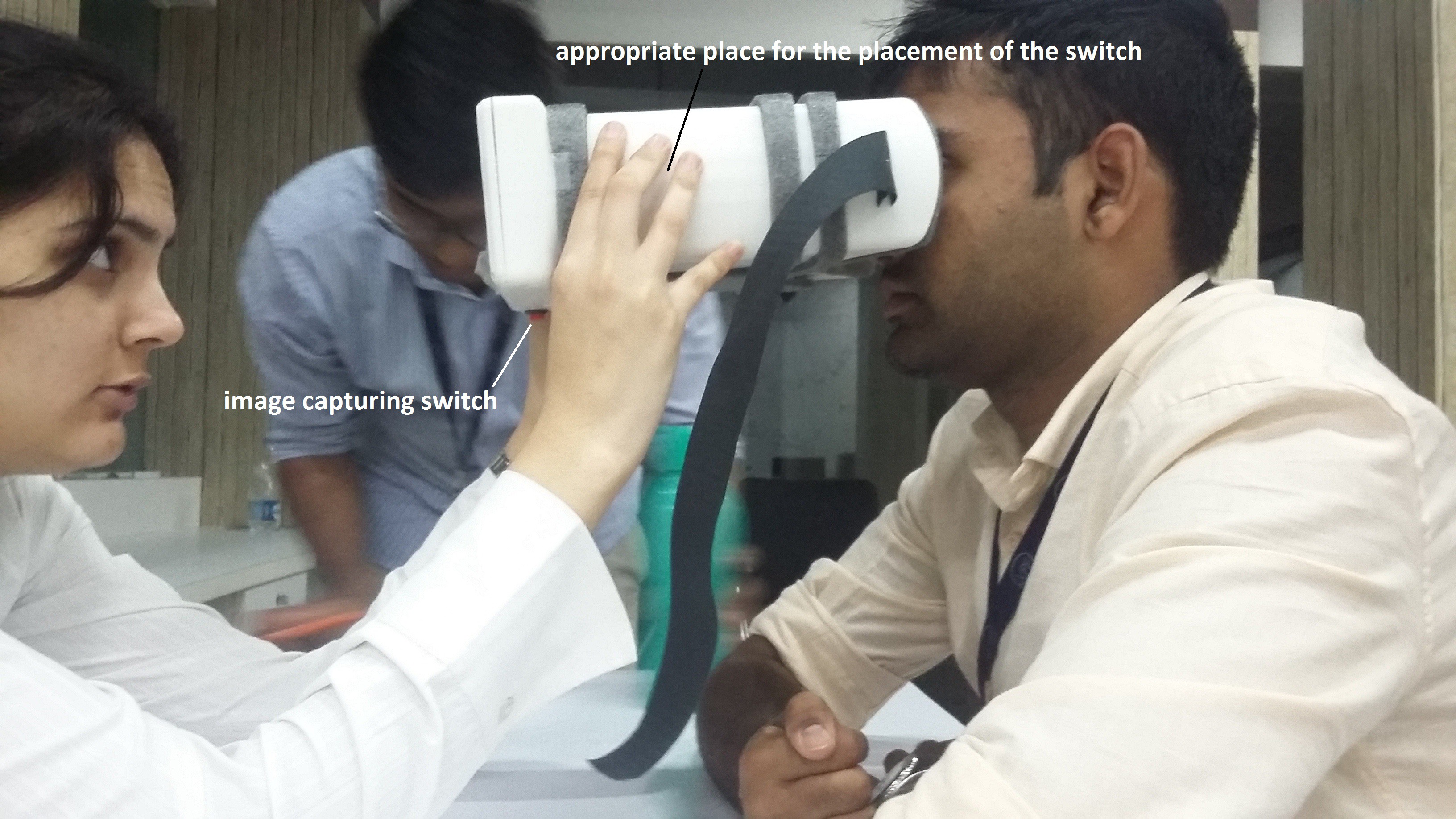
- Image capturing switch is too far from the screen and is not easily accessible
while taking the picture. The device front part is bulkier than the palm so
reaching for the touch screen is a bit difficult with simultaneously focusing the retina and taking the image.
![]()
- Heat buildup due to processors running on camera and Rpi. So vents have to be provided on the outer surface for convective heat transfer through air.
The focusing issue:
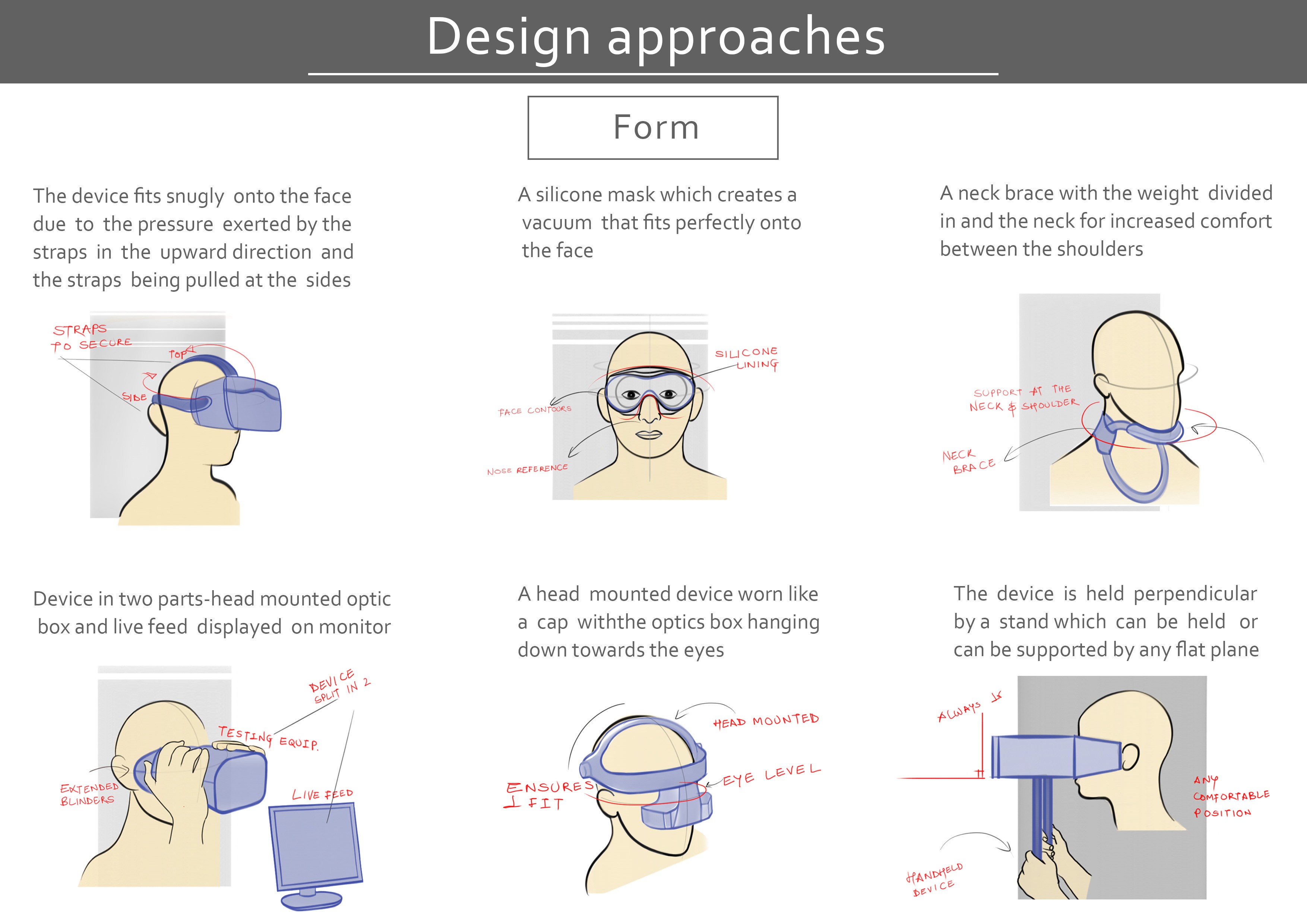
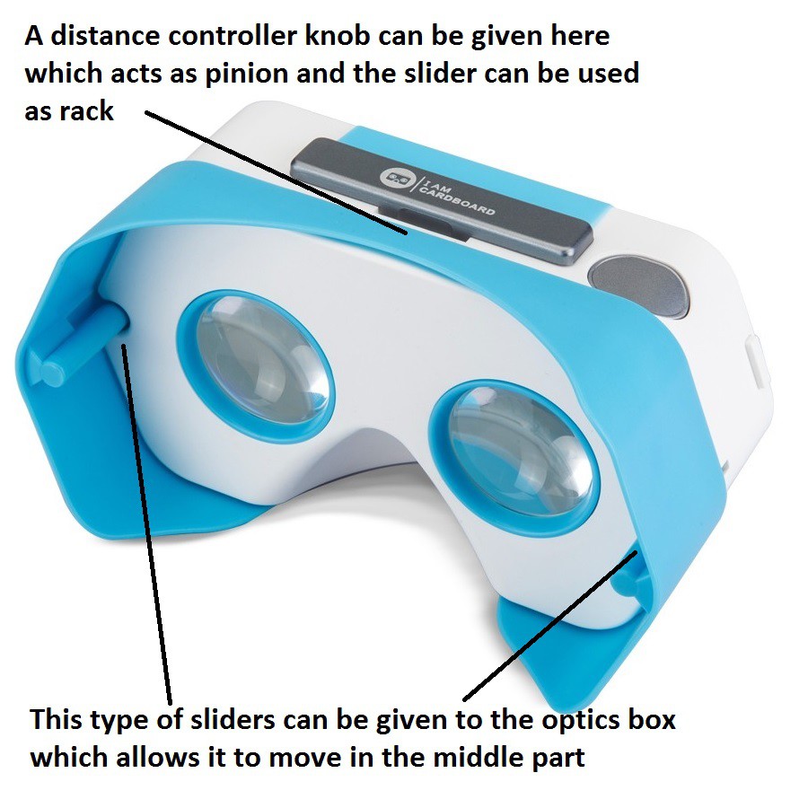
- Same problem as in VR headgear, because of different refractive
errors the lens should be moved front and back to get the retina in camera's
focus. In our case the lens alone shouldn't be moved as it changes the field of view
of retina. The whole optics box has to be moved to compensate for the
refractive error. This can be achieved by adding a sliding mechanism to the box
and a rack and pinion mechanism to control the distance between the eye and the
lens.
![]()
Device orthogonality with the examinee:
- While capturing the image the objective lens(20D) plane has to be
parallel to the subject's eye lens plane. In the present prototype this is not
happening because of uneven mass distribution towards the back.
![]() If not parallel we get distorted images of the retina as the camera and light won't focus the retina properly. By keeping the device orthogonal to the examinee we can ensure the planes of 20D lens and lens of the eye are parallel to each other.
If not parallel we get distorted images of the retina as the camera and light won't focus the retina properly. By keeping the device orthogonal to the examinee we can ensure the planes of 20D lens and lens of the eye are parallel to each other.![]() It can be done by two methods one by adding a headband as normally used in VR headgears. Other option would be arranging components in such a way it redistributes the whole weight and achieve orthogonality as keeping an head band with the device needs sterilization every time after use and feels little invasive for the patient.
It can be done by two methods one by adding a headband as normally used in VR headgears. Other option would be arranging components in such a way it redistributes the whole weight and achieve orthogonality as keeping an head band with the device needs sterilization every time after use and feels little invasive for the patient.
Selecting proper prototyping technique:
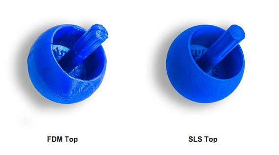
- Present prototype was made on an FDM 3D printer. After printing on an FDM printer we
need to remove supports and excess plastic either with cutting tools or
grinding tools. Lot of postprocessing has to be done in getting smoother
surface. This causes uneven dimensional tolerances. Once we add the sliding mechanism
and three piece assembly device the surface should be really smooth for movements and ease of assembly. This can be overcome by printing those parts
with an SLS printer.
![]()
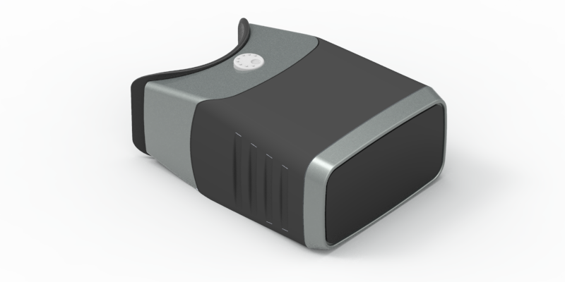
Mockup
![]()
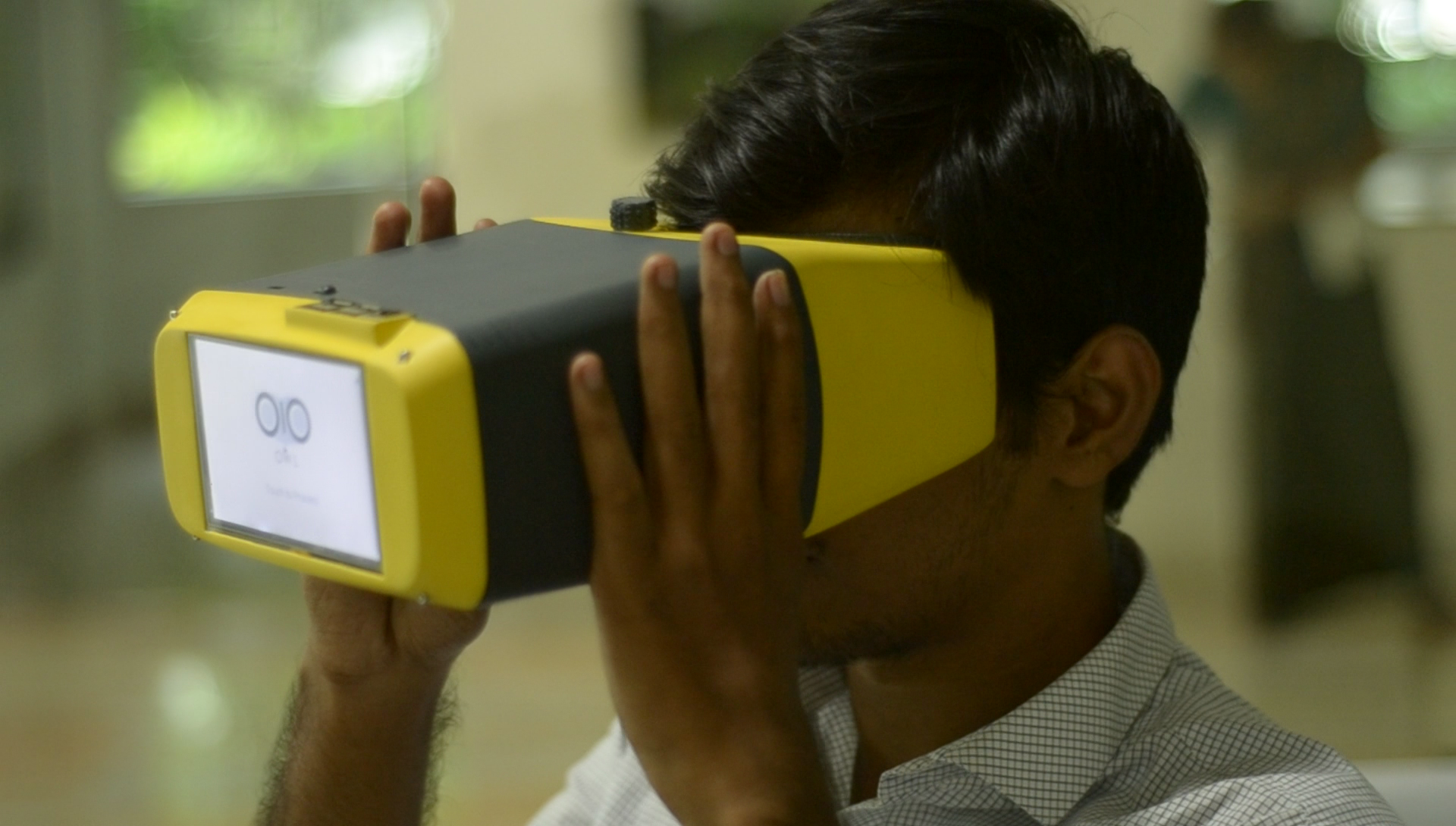
Open Indirect Ophthalmoscope
An open-source, ultra-low cost, portable screening device for retinal diseases















 Click Switch
 Click Switch Assembled inside the middle casing





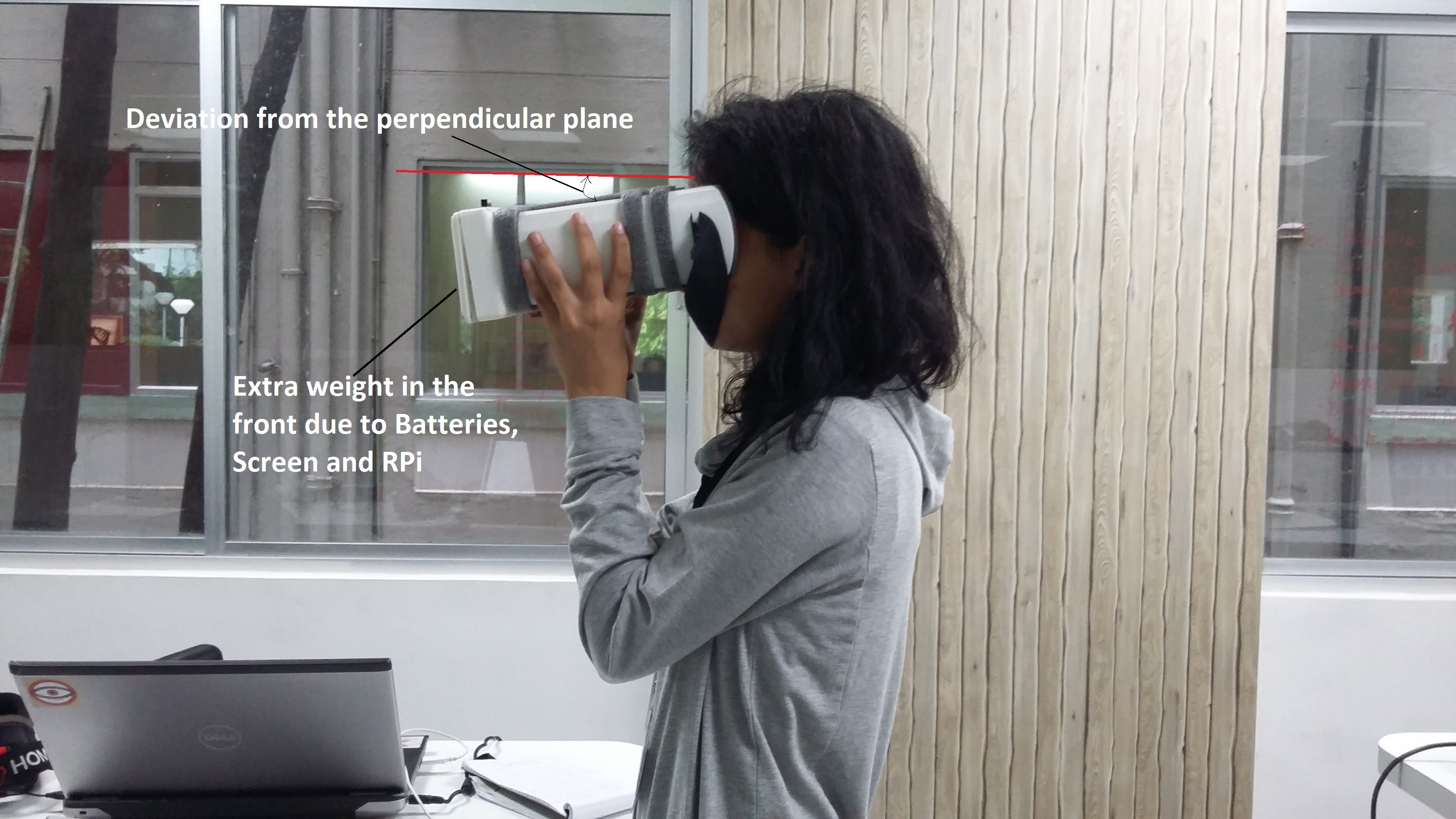 If not parallel we get distorted images of the retina as the camera and light won't focus the retina properly. By keeping the device orthogonal to the examinee we can ensure the planes of 20D lens and lens of the eye are parallel to each other.
 It can be done by two methods one by adding a headband as normally used in VR headgears. Other option would be arranging components in such a way it redistributes the whole weight and achieve orthogonality as keeping an head band with the device needs sterilization every time after use and feels little invasive for the patient.