I have yet to check the schematic for errors so I will wait until I do that to post it, but I spent a little time doing up a design based on topology 3.
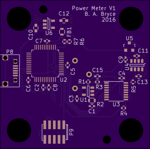
I used a lot of 0402 parts. I did this largely to minimize the signal path length between the critical analog components. The photodiode goes on the back of the board if you are wondering it is the 3 holes in the exact center of the PCB.
U2 is the transimpedance amplifier. U3 is the PGA/Instrumentation amplifier. U4 is the ADC. U5 is the voltage reference.
Overall I'm happy with this as a first cut. I think I can remove the pull-up resistors for the I2C based on the manual of the ATSAMD21 but I put them on there to be safe. I could and still may reduce the size of the board by moving the microcontroller to a 5x5 QFN package and removing the standard 1.27 pitch ARM SWD/JTAG header (P9).
Maybe I will make a little locking pogo pin fixture.
Discussions
Become a Hackaday.io Member
Create an account to leave a comment. Already have an account? Log In.