Target specifications:
Wavelength range: 400-1000 nm
Power range: 50 nW - 50 mW (higher with ND filters)
Accuracy: better than 1% for most of range
Sensor size: 4 mm diameter circle
Interface: Virtual serial port
Optical post: Metric or Imperial
A simple USB silicon pin photodiode based laser power meter
To make the experience fit your profile, pick a username and tell us what interests you.
We found and based on your interests.
Target specifications:
Wavelength range: 400-1000 nm
Power range: 50 nW - 50 mW (higher with ND filters)
Accuracy: better than 1% for most of range
Sensor size: 4 mm diameter circle
Interface: Virtual serial port
Optical post: Metric or Imperial
One of the parts on the board, the DAC, has a package that is called SOT-23-8.. In my haste in making it I took no notice of the pitch of the pins presuming that it was the same as a SOT-23-5 or SOT-23-6. Alas it is not. In fact the part is 0.65 mm pitch but with the size of a SOT-23. And so although I received my PCBs for this first version I can put them to no good use. I have sent out a revised PCB as a result. With luck I shall have something by mid-July to test.
I could of course bodge something but given all the other pulls on my time it will have to keep until the real testing can be done with a real board.
So the parts for the first prototype are here but the boards will take a bit more time.
When I broke open the box, I took a good look at the pin diode. Though its rather comparable to commercial detectors it is a bit smaller.
The diode would be easier to use if it were larger area, the problem is that area costs money (and dark current). 60-100 dollars a sensor would get a 30 sq. mm to 100 sq. mm detector. This being an order of magnitude more isn't that appealing. Nevertheless it is possible.
I also note that in the smaller detector realm there is a reasonable choice from Thor Labs that you can get with a NIST calibration ($$$) or without (reasonable). It might be interesting to build a version compatable with that footprint to gain a NIST traceable result.
Probably the better solution to the size of the detector is just to use single convex lens. The system will already be compatible with a lens tube and thus one can get an effective diameter of 25 mm if a lens is used (presuming the laser is reasonably collimated coming in). Using a lens does introduce another offset/loss to correct for, but that loss is published and so should not be too hard to remove either.
It will be interesting to see what kinds of calibration and accuracy I can develop with this detector when the boards arrive.
I have sent out the first iteration of the design to OSHpark for fabrication. I wanted to get it out the door to have a basic meter available as quickly as possible. My available time will quickly go to zero once August arrives.
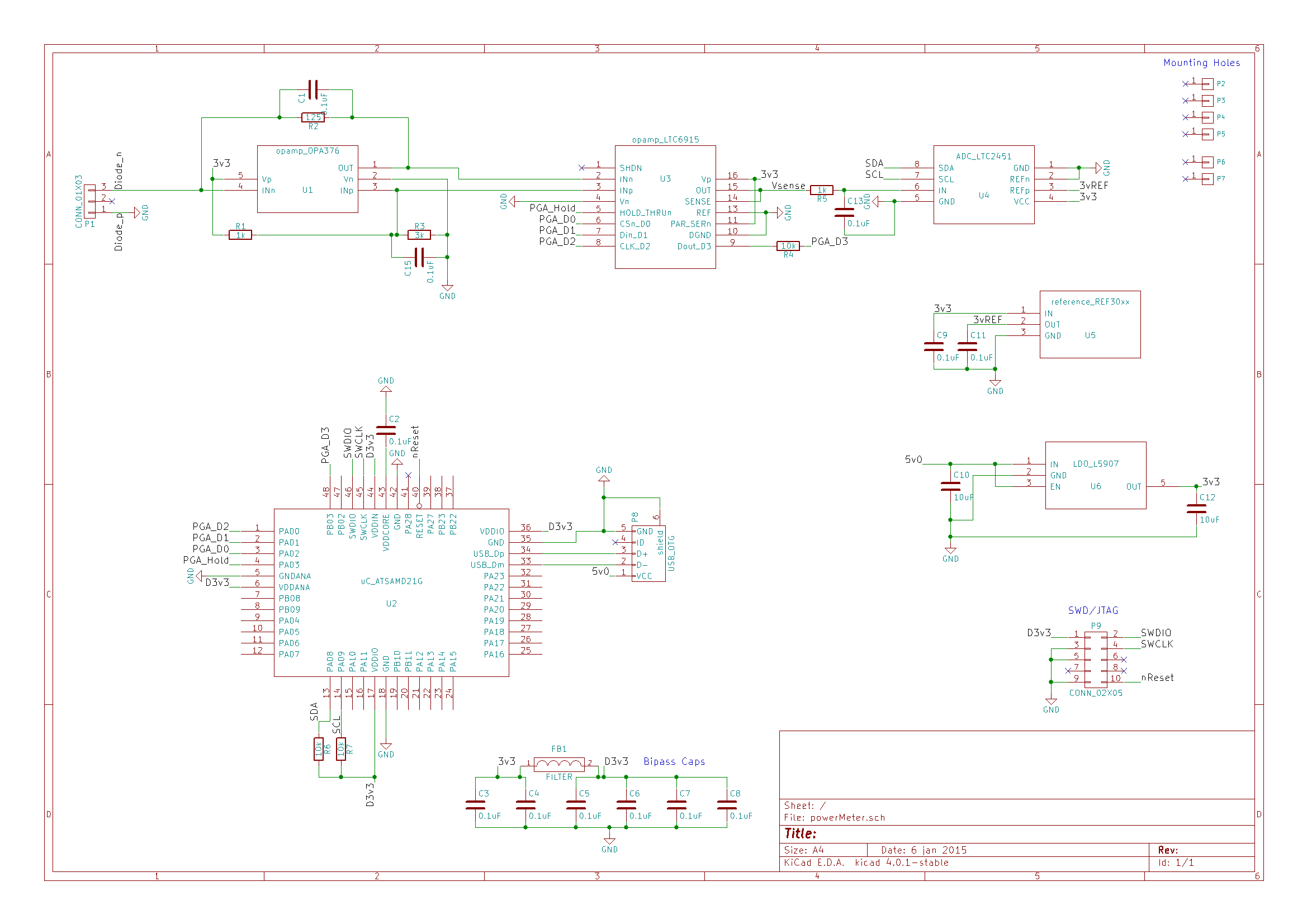
I added one pull-up resistor to the reset pin but in my quick look over today everything else seemed okay.
Should have everything in a couple weeks to try it out.
I have yet to check the schematic for errors so I will wait until I do that to post it, but I spent a little time doing up a design based on topology 3.
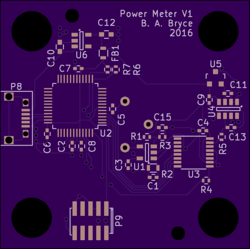
I used a lot of 0402 parts. I did this largely to minimize the signal path length between the critical analog components. The photodiode goes on the back of the board if you are wondering it is the 3 holes in the exact center of the PCB.
U2 is the transimpedance amplifier. U3 is the PGA/Instrumentation amplifier. U4 is the ADC. U5 is the voltage reference.
Overall I'm happy with this as a first cut. I think I can remove the pull-up resistors for the I2C based on the manual of the ATSAMD21 but I put them on there to be safe. I could and still may reduce the size of the board by moving the microcontroller to a 5x5 QFN package and removing the standard 1.27 pitch ARM SWD/JTAG header (P9).
Maybe I will make a little locking pogo pin fixture.
Given the current limits of the ICs involved, it is worth taking another look at the possibility of doing without them. This was discussed previously with this very simple topology:

Here the reverse bias on the diode is a function of the current. Let the reverse bias be Vbias. If the diode would become forward biased at the max laser intensity we expect then at 1/10 the light intensity the reverse bias would be 9/10 of Vbias.
Why does the reverse bias matter? Because in a pin photodiode the electric field helps get electrons and holes out of the device. If there is a lifetime for the carriers in the diode then they will relax back to equilibrium (i.e. lost to us) with a characteristic time, that is:
The time spent in the junction if dominated by field assisted transport is directly proportional to the voltage if the field drops only over the intrinsic region of the semiconductor/diode.
The validity of this assumption can be seen by if the capacitance of the diode is changing as a function of bias.
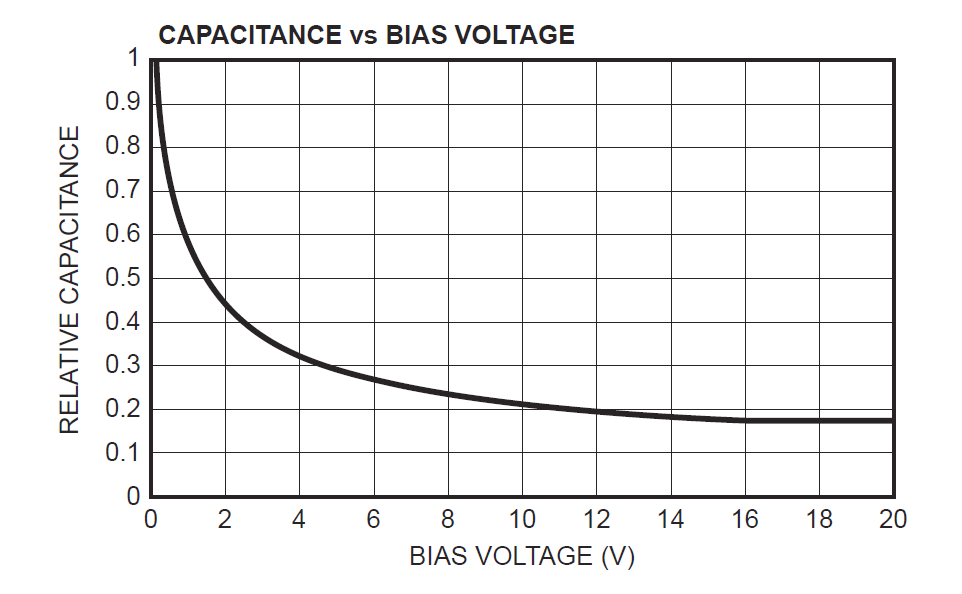
For the diode we have selected for a large reverse bias this is pretty much true but for a reverse bias between 0 and 5 V it certainly is not true.
However for the moment we shall assume that it is true. Further we will make another assumption that we loose exactly 1/e of he carriers at 1 V reverse bias, and that at this bias we are already field transport dominated.
This is quite a lot of assumptions but not totally unreasonable. In a pin diode the i region is fairly thick and does most of the absorbing. So diffusion based transport is less important. Because the i region is thick and low doped most of the field does fall across it. We know the pin photodiode gets most of the carriers out because it would be a terrible detector if it did not and we know it is possible to do experimentally.
So with all of these assumptions, what happens if we double the voltage, well then we cut the time in half. We do about 23% better. This would be a significant difference.
If on the other hand at 1 V the transit time is 1/3 of the lifetime then we have about 95% of the carriers collected and 2 V would make it 99.8%.
So does the bias changing on the diode matter? It could be huge error or a tiny one. The good news is that it can be measured, the bad news is that it is a function of how much light you put in too as that moves the quasi-fermi levels around. Even if the external voltage of the device is carefully fixed the field distribution inside the diode will still change some with the injection level.
Given the issues with sinking currents this topology might be worth revisiting for its simplicity.
When I wrote the first analog design log entry I proposed 4 topologies that might be used to solve the problem.
I decided quickly that not having a constant reverse bias on the diode could lead to sticky issues with the response function also being a function of the input power.
So I started to look at buffered designs based on transimpedance amplifiers. All well and good except I overlooked something at 3 AM and that is that the amplifiers have finite output resistance (of course). They can only source or sink a few mA or perhaps 10s of mA. Indeed the chosen zero offset amplifier from LT can only sink 2 mA for a supply around 3 V. For the power range we would need to sink up to 100 mA. The good news is that LT6230 which was chosen for the last topology can source/sink at least 25 mA. With a typical value of 40 mA. OPA378 is similar at 30 mA so all together this means that the feedback resistance will need to be set to something more on the order of 100 ohms rather than 50.
OPA376 also looks like a good alternative. It has a typical offset voltage of 5 uV and noise of 0.8 uVpp in 0.1-10 Hz. It can source 30 mA and sink 50 mA. It has higher offset drift than OPA378. AD8615 looks like a possible choice as well though at much greater offset, it can drive a massive 150 mA! AD8615 is probably a better choice for the 4th topology and OPA376 is probably the best part I have found for the 3rd. Flattening the sensitivity function of the detector by choosing a detector coated to do better in the near-UV would improve the high power headroom as well.
If we wish to self-limit the amplifier to a drive of 30 mA with a supply of 3.3 V then the feedback resistance should be nominally 110 ohms rather than 50. For a sensitivity function peaking at 0.7 A/W, this would correspond to a laser power limit of just over 40 mW (280 mW for the best case). If the noise floor in band is of order 1 uV, then this corresponds to current of 9 nA or about 3 times the dark current. For a sensitivity of 0.1 A/W this is a should mean a minimum detectable power of about 90 nW (12 nW for the best case).
With the first cut electronic design largely squared away conceptually, I turn to the physical mounting of this power meter.
The expensive commercial power meters tend to have heatsinks on them to stabilize the detector. This could be a problem at high powers for the current design but it won't be clear until it is built.
Apart from dissipating heat the system has to be mounted to an optical post. In the past I have taken the approach of using a cage plate and tapping it to mount the PCB.
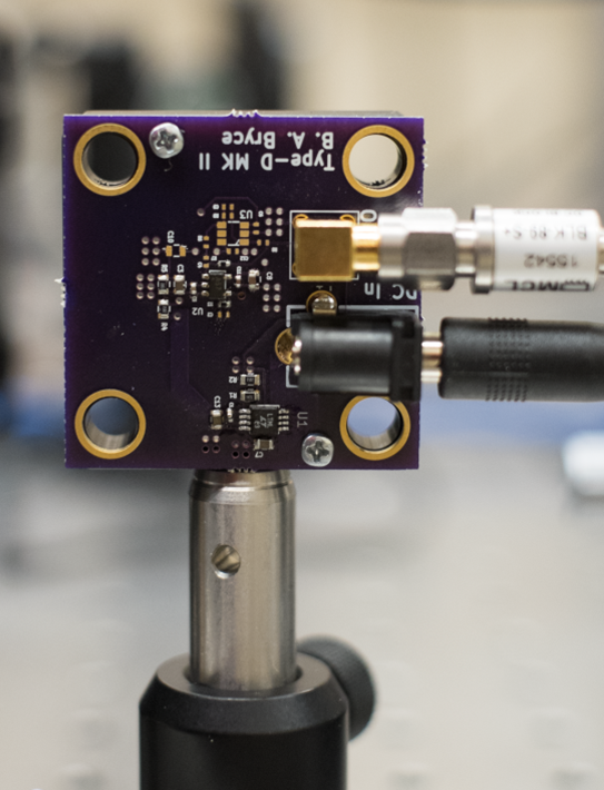
Here is an example of an amplified photodetector I did in the past.
In the current device I will probably use an SM1 thread cage plate, which is available for imperial and metric posts. This will allow lens tubes or mounted optics to be used with the power meter, which will simplify the use of neutral density (ND) filters use or focusing optics if the beam diameter is larger than 4 mm.
My standard mounting method is not shielded but a cover could be produced at need.
In this update I will consider the analog and digital aspects of the analog front-end discussed in the previous log entry.
We need to resolve currents on order of 10 nA to 60 mA. The front-end design did this by converting this to a voltage via an effective resistance of nominally 50 ohms.
This results in voltages from 500 nV to 3 V. The instrumentation amplifier chosen has settable gain in powers of 2 from 1 to 4096. Thus for the minimum voltage with the maximum gain, will become just over 2 mV.
If the reference for the analog to digital converter (ADC) is 3 V and we had a perfect 16-bit then we would be able to resolve voltages in nominally 45 uV steps.
ADCs are not perfect though. They have properties like integral non-linearity, differential non-linearity, the voltage reference will have a percentage error, and more. Nevertheless to resolve 2 mV should only require a perfect 12-bit ADC.
Getting an effective number of bits of 12 out of 16 should not be an impossible task. For our initial design we will choose LTC2451 for this purpose. We will use an external 0.2% accurate 3V voltage reference.
With the ADC taken care of the signal is now digital and any solution that gets the digits to a computer is basically equivalent. So the choices here are far more arbitrary.
I am currently using a lot of ATSAM parts for projects and have some code already worked up for simple virtual serial sensor applications. As a result I will select ATSAMD21 for the microcontroller. We will start with the G15B flavor as 32 KB should fit everything easily, but if we need more space there are larger one available.
The virtual serial port will allow reading the current power and storing calibration data on the particular module via simple ASCII based commands. I will write a python library to encapsulate the functions.
The simplest command set would be:
r - read the current current level
c - read the calibration table
w - write the calibration table
Everything else could be taken care of in the python library.
A final note is that the ATSAM series all contain ADCs. The SAMD21 contains a 12-bit ADC, but its accuracy is not great and its effective number of bits is around 9.5. Given the cost of the mechanical parts of this system an external higher performance ADC probably makes more sense.
Now that we have a transducer (subject to change of course), we have to use that transducer to convert light into a number displayed on a computer screen.
There are two parts of that solution: the analog part and the digital part. In this entry I will just focus on the analog part because that is the more tricky part.
The big issue with this sort of power sensor is the dynamic range of the signal.
We need to measure signals from say 10 nA to 10 mA. That is 6 orders of magnitude. There is more than one way to attempt to solve this problem. Like most engineering problems there are advantages and disadvantages to each solution.
Whenever I see the phrase "orders of magnitude" I immediately think: log. After all if I need to plot a signal that ranges over orders of magnitude I will probably use a log scale.
As mentioned in previous in these logs the photodiode is essentially going to be a current source. If we could create a circuit that created a voltage that was proportional to log(I) then we could "compress" the dynamic range of this measurement.
Logarithmic amplifiers do exist. One log-amp I have used in the past is LOG101. It is a cool circuit.

If we wanted to use LOG101 to solve our problem the circuit topology is pretty simple. We reverse-bias the photodiode and feed the current into the log-amp, which converts the current into a voltage which is then sampled by an ADC and sent to the digital part of the circuit using I2C in this case.
At first glance it seems a great solution. The tripping points to implementing this idea largely are in making a precision reference current for the log-amp. If you take a look at the LOG101 datasheet you will see the output is actually the log of the ratio of two currents, one of which is the reference.
The other downside to using LOG101 is that it is a dual supply circuit. If this device is to be powered over USB then only +5V is available. DC-DC conversion can be used to create a -5V supply (probably using a charge pump) but it certainly would complicate the system, cost more and potentially be noisy (it can be a task unto itself to get switch mode power cleaned up nicely for such a sensitive measurement).
Let's return to the original problem, we need measure a signal that ranges over 6 orders of magnitude. One way to look at this problem is how many bits is that? This is log2(1e6) which is about 20-bits.
Log-amplifiers are nice but modern analog to digital converters (ADCs) have huge dynamic ranges. They are available in 24-bit flavors. In principle this means just a resistor and an ADC could solve the problem. In practice the input to an ADC should at least be buffered.

Taking this view it is possible to come up with this circuit. The amplifier (U1) is an instrumentation amplifier. Resistors R1 and R2 take the current from the photodiode and turn it into a voltage. If the value of R1 is well known then the current is known and from the sensitivity function then the power incident is known. The value of R2 may be 0 or it may be some fraction of the total resistance R (R = R1 + R2). If we place the negative terminal of U1 at the rail (0 V) then my suspicion is that performance will not be as good as if it is lifted off the rail slightly. This is the point of R2. Amplifiers can be rail-to-rail, but near the rails performance will never be as good. R1 sets the V/A gain, it is limited by the maximum current we expect to have output from the photodiode. This is of order 100 mA, given our rail (without DC to DC conversion) is at most 5V this implies 50 ohm is the nominal maximum for R.
If the instrumentation amplifier had a fixed gain this would also mean that it must be set low enough that the output voltage is acceptable to the ADC (which will have an input voltage range). Because 5V is the absolute maximum voltage in the system this implies a gain of 1. Thus we would have to rely solely on the ADC for the needed dynamic range (20-bits).
This is possible but a better way would be to pick an instrumentation...
Read more »Power meters use a few flavors of sensor: thermopiles, pyroelectric, and photodiodes are the most common.
Thermopiles and pyroelectric sensors basically rely on turning the light that hits them into heat and then inferring the laser power by how much the sensor has heated. From a laser *power* point of view this is nice, because they are not that sensitive to what wavelength the light is save for the variation in reflectivity of the sensor.
Photodioes are a bit more tricky. Lasers have a wavelength, and with that wavelength an energy per photon:So the energy per photon is Planck's constant * the speed of light / wavelength.
Photodiodes count photons, not energy.
To get the photon into the photodiode one must couple the light into the semiconductor crystal to have a chance to absorb the light. Some of the incident light will be reflected.
The
amount of a wave that is reflected from any interface between two
materials depends on the impedance mismatch between the two materials.
In optics the typical way to parameterizethe
impedance is the index of refraction. The index of refraction of
silicon is around 3.4, and the index of refraction of air is nominally
1. Fresnel's equations allow
the calculation of how much light will reflect off the surface. To
minimize this problem photodiodes are anti-reflective coated. Light
photovoltaic solar cells this often makes them look blue. The
anti-reflective coating is a thin film that typically is a quarter
wavelength of the wavelength of light the user most cares about.
If the photon goes into the semiconductor that makes up the diode it might get absorbed. The probablity of this increase the larger the energy of the photon. If it is absorbed it creates an electron-hole pair. If that electron-hole pair makes it out of the diode you get some current.
All of these considerations result in a optical response function for a photodiode. A typical response for a silicon photodiode is shown below:
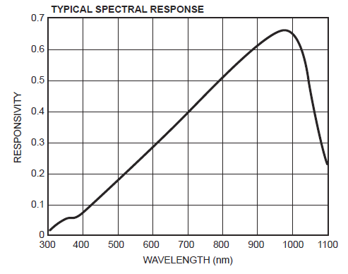
The response above is that of ODD-12W. Which is fairly typical of a silicon photodiode. Different anti-reflective coatings shift this around a bit. The responsivity of the diode is often plotted in A/W, here it is a relative scaling of A/W with respect to a fixed point at 632 nm where they report a typical value of 0.40 A/W.
The function peaks at high wavelength because for each W of power at those wavelengths there are more photons. The silicon meanwhile absorbs them less well, and the reflectance off the surface of the diode changes. These are the three main factors that produce the shape above.
If we want to use a photodiode to measure the power of a laser we must know the responsivity of the photodiode well at that wavelength. This almost certainly mean that the laser power meter will need calibration to be accurate. Although the datasheet's curve will get us close.
The reason I will choose to use a photodiode for this project is mainly because they are easy to work with and inexpensive. The main downsides are this complex responsivity function that requires careful calibration.
The photodiode I have initially settled on is ODD-12W. The characteristics I have looked for in my photodiode are:
(1) Low cost
(2) Large area
(3) Low dark current
The first is self-explanatory. The second is helpful if the laser beam gets large. Commercial power meters look to have photodiodes with diameters on order 6 mm. While these do exist from electronic part suppliers they are substantially more costly, as I result I choose a 4 mm diameter photodiode.
The laser parameter is the dark current. This is the current that the photodiode supplies when it is reversed biased and there is no light. Essentially it is scaling factor in the Shockley equation.
The reason it is important is that it represents a noise level of current that the diode produces. For the ODD-12W the typical value of dark current is 3 nA. This will set a lower bound on our ability to detect the laser power. Near 400 nm the responsivity function is nominally 0.1...
Read more »
Create an account to leave a comment. Already have an account? Log In.
Become a member to follow this project and never miss any updates
 Paul Andrews
 mihai.cuciuc
 jbb
jbb
 Jakob Wulfkind
I added a background photo of a pretty HeNe laser with an unshielded gas discharge tube. Thanks to Tommy Markstein/Wikipedia for supplying it!