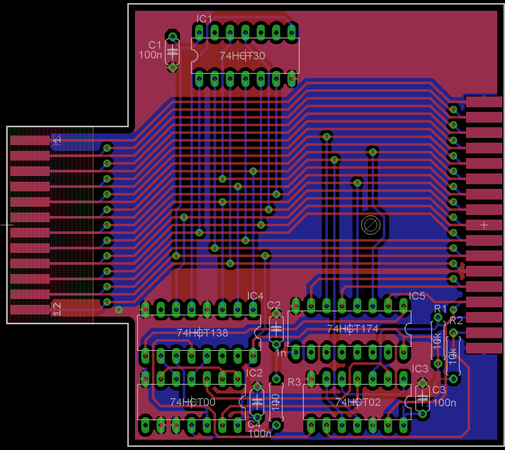
I've just routed the PCB for the bankswitch cartridge. The routing was manually done and it took some time to optimize the disposition of the TTLs as well as the pins and gates of the NAND and NOR chips so the board can easilly be built at home (or in cheap PCB manufacturing services). All tracks are 16 mils and no unnecessary via have been used.
 There are still some room for improvement ,though.
 danjovic
Discussions
Become a Hackaday.io Member
Create an account to leave a comment. Already have an account? Log In.