The Bankswitch cartridge implements the three most common schemes named F8, F6 and F4. The working of the bankswitches is depicted on the table below.
Address  -Address Lines--   Bankswitch/Bank selected
         1 11               8K    16K   32K
         2 1098 7654 3210   F8    F6    F4
$1FF0 0001 1111 1111 0000   -     -     -
$1FF1 0001 1111 1111 0001   -     -     -
$1FF2 0001 1111 1111 0010   -     -     -
$1FF3 0001 1111 1111 0011   -     -     -
$1FF4 0001 1111 1111 0100   -     -     0
$1FF5 0001 1111 1111 0101   -     -     1
$1FF6 0001 1111 1111 0110   -     0     2
$1FF7 0001 1111 1111 0111   -     1     3
$1FF8 0001 1111 1111 1000   0     2     4
$1FF9 0001 1111 1111 1001   1     3     5
$1FFA 0001 1111 1111 1010   -     -     6
$1FFB 0001 1111 1111 1011   -     -     7
$1FFC 0001 1111 1111 1100   -     -     -
$1FFD 0001 1111 1111 1101   -     -     -
$1FFE 0001 1111 1111 1110   -     -     -
$1FFF 0001 1111 1111 1111   -     -     -
Then:
- F8 bankswitch uses 2 regions of 4K selected by bit 0 of the address lines.
- F6 bankswitch uses 4 regions of 4K selected by bits 3 and 0 of the address lines.
- F4 bankswitch uses 8 regions of 4K selected by bits 3, 1 and 0 of the address lines.
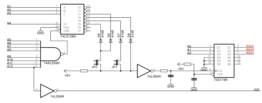
By using two configuration pins it is possible to force the levels of address lines 3 and 1 at the input of the bankswitch register in order to select the desired scheme. By forcing A3 and A1 it is possible to use the F8 scheme (8K). For 16K games A1 is kept constant and the bankswitch is the F6. At last, if neither A3 nor A1 is selected the F4 bankswitch enables the use of 32K games.
Schematic:
The schematic of the bankswitch is on the picture below. Notice the delay RC network from the output decoding to the address latch as well as the reset circuit on the /CLR pin of the LS174.
Bankswitched cartridge connector:
The bankswitched cartridge connector inherits the pinout of the original cartridge but has some extra pins for the extra address lines A12~A14 as well as a pre inverted A12 (Chip select). It has also two bankswitch selecting pins.
The bankswitch scheme can be selected by connecting the jumpers
 JP1     JP2   ROM Size
 open    open   8K (F8)
 close   open  16K (F6)
 close   close 32k (F4)
                               +------+
                         /BSF8-|1   34|-
                         /BSF6-|2   33|-
                         /BSF4-|3   32|-
                      /A12 /CS-|4   31|-AA13
      +------+            AA12-|5   30|-AA14
   A7-|1   24|-sGND         A7-|6   29|-sGND
   A6-|2   23|-VCC          A6-|7   28|-VCC
   A5-|3   22|-A8           A5-|8   27|-A8
   A4-|4   21|-A9           A4-|9   26|-A9
   A3-|5   20|-A11          A3-|10  25|-A11
   A2-|6   19|-A10          A2-|11  24|-A10
   A1-|7   18|-A12          A1-|12  23|-A12(not bankswitched)
   A0-|8   17|-D7           A0-|13  22|-D7
   D0-|9   16|-D6           D0-|14  21|-D6
   D1-|10  15|-D5           D1-|15  20|-D5
   D2-|11  14|-D4           D2-|16  19|-D4
  GND-|12  13|-D3          GND-|17  18|-D3
      +------+                 +------+
Particularities of the 32K cartridge
Due to the fact that the lines A12,A13,A14 are not consecutively connected to A0,A1,A3 but to A0,A3,A1 the blocks 2 to 5 on the 32K cartridge appear to the game out of its sequential order on the ROM.
Instead of blocks: 0,1,2,3,4,5,6,7 (A12<=A0, A13<=A3, A14<=A1)
we have the blocks: 0,1,4,5,2,3,6,7
To workaround this issue there are two alternatives:
- Split the ROM file into 8 chunks of 4K and reorder them in the 0,1,4,5,2,3,6,7 order
- Switch the lines A13 and A14 in the ROM cartridge
 danjovic
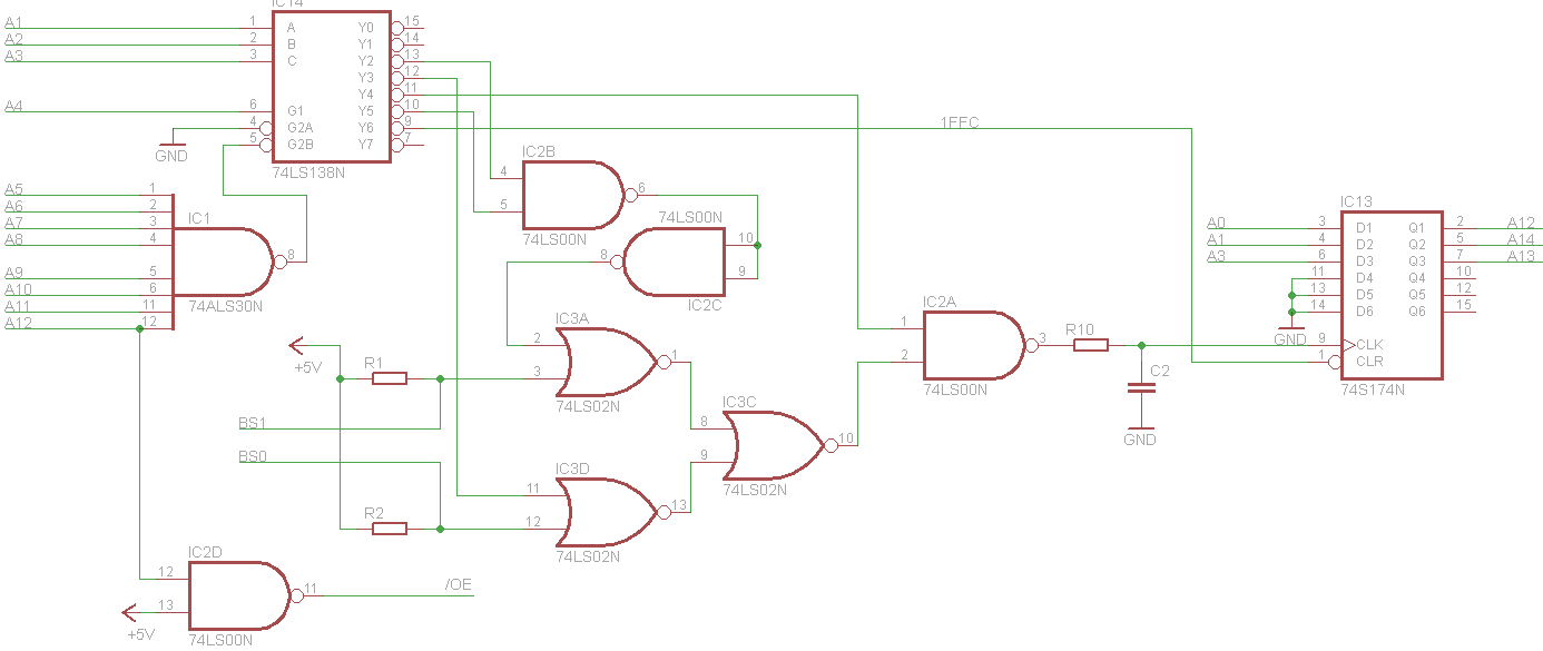
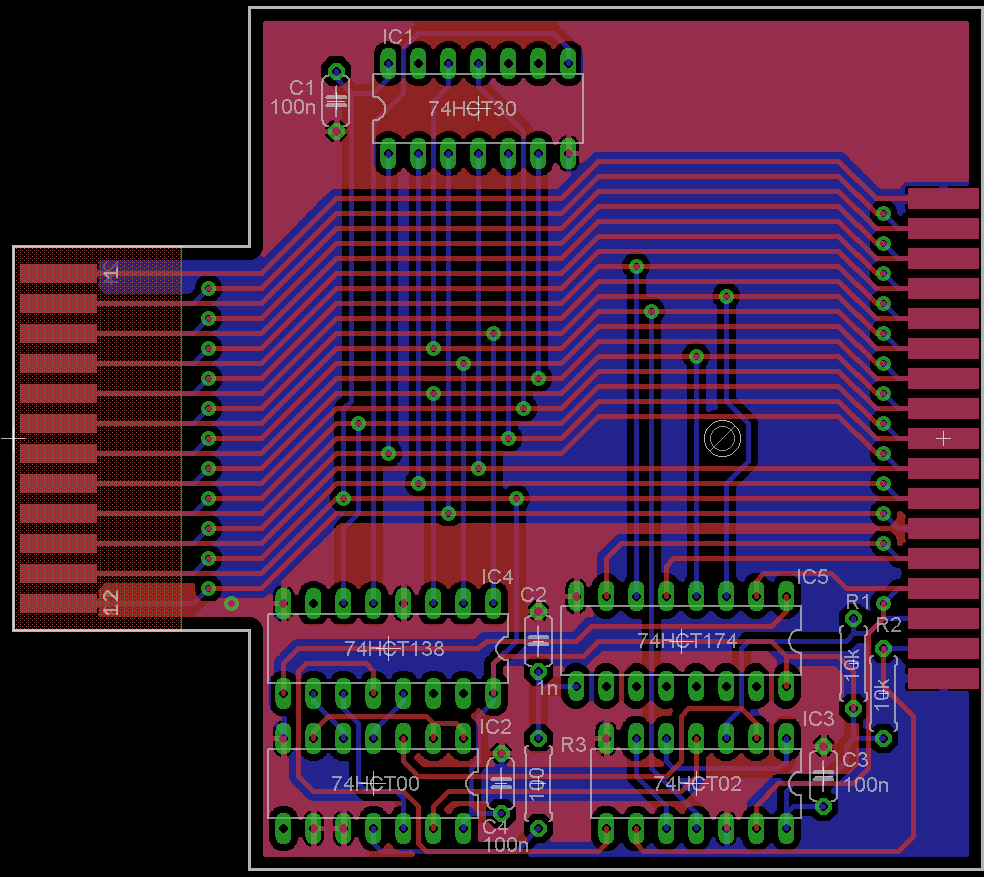 There are still some room for improvement ,though.
 Pascal
 Eric Wright
A matrix decoder could be created with a latching device and another EPROM to create any sort of addressing method you pleased, including 1K banks remapped to any address range. as well as masking out unusable address space, for example creating an overlay mask for the lower 4KiB of address space below the normal cart range by preventing EPROM data output at specific addresses to prevent bus collisions. while using a pair of EPROMs the overall parts count would be reduced the advantage here is the simple method of changing the addressing system involving minimal if any board changes.