danjovic
-
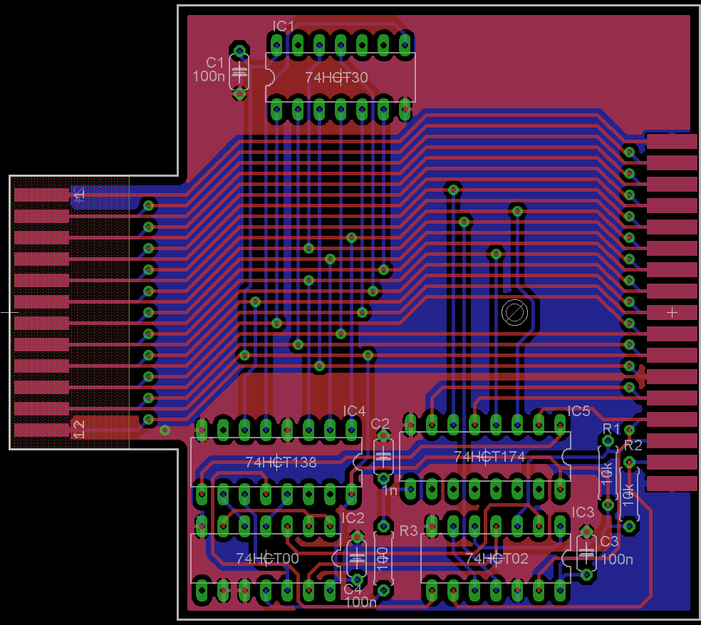
Hand Routed PCB
09/03/2016 at 19:24 • 0 commentsI've just routed the PCB for the bankswitch cartridge. The routing was manually done and it took some time to optimize the disposition of the TTLs as well as the pins and gates of the NAND and NOR chips so the board can easilly be built at home (or in cheap PCB manufacturing services). All tracks are 16 mils and no unnecessary via have been used.
![]() There are still some room for improvement ,though.
There are still some room for improvement ,though. -
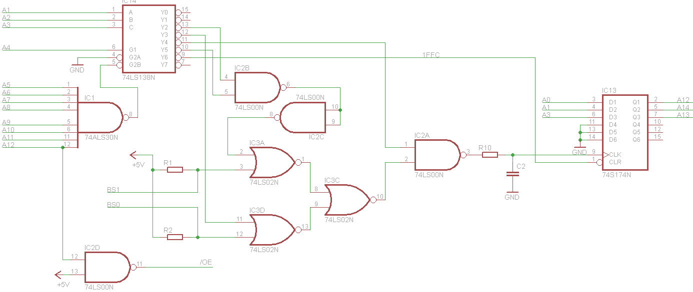
Updated schematics
08/04/2016 at 02:34 • 0 commentsUpdated the schematics to allow bankswitch selection from external logic levels on BS0,BS1 pins instead of simple wired-or configuration. One chip was added but 4 diodes and three resistors were eliminated.
![]()
A PLD version is also being considered. It will be considerably simpler to implement, but without the same retro appeal.
Atari 2600 Bankswitch Cartridge
A ROMless cartridge with internal selectable bankswitch for 8/16/32K games and a DIY ROM friendly connector.
 There are still some room for improvement ,though.