-
Some samples made with Printem
08/23/2016 at 00:07 • 0 commentsThis video should detail a bunch of sample made with the Printem film
We are in the process of creating more build logs and detailed instructions for people to create and try out some films, we also have a bunch of samples that we made for testing, will be glad to send them to anyone interested as well.
-
How the Printem Film works ?
08/23/2016 at 00:04 • 0 commentsIt is recommended that you follow the project logs in chronological order.
So how does the Printem Film work ? It uses the selective adhesion of the copper to the substrate using the UV adhesive to "tear away" only the copper in the right places to form the circuit. The diagram below illustrates this
![]()
a) The home/office printer prints black ink onto the acetate substrate, the PCB pattern is printed in negative, meaning that only the areas with the copper traces are left transparent and everything else is printed on .
b) When this is exposed to UV light, the printed ink blocks it from passing through, so only areas without the ink allow the UV light to pass through. The light then passes through the substrate ( which is UV transparent ) and cures the UV adhesive only in the areas directly underneath the unprinted areas.
When the UV adhesive cures in response to this exposure, it strongly adheres to the copper foil below it
c) When the layer is peeled away, it "pulls" only the desired copper with it, leaving the rest attached to the peel-off layer and then being discarded.
d) Now the PCB is ready to be used
The next post details some examples made with Printem
-
Construction of the Printem Film
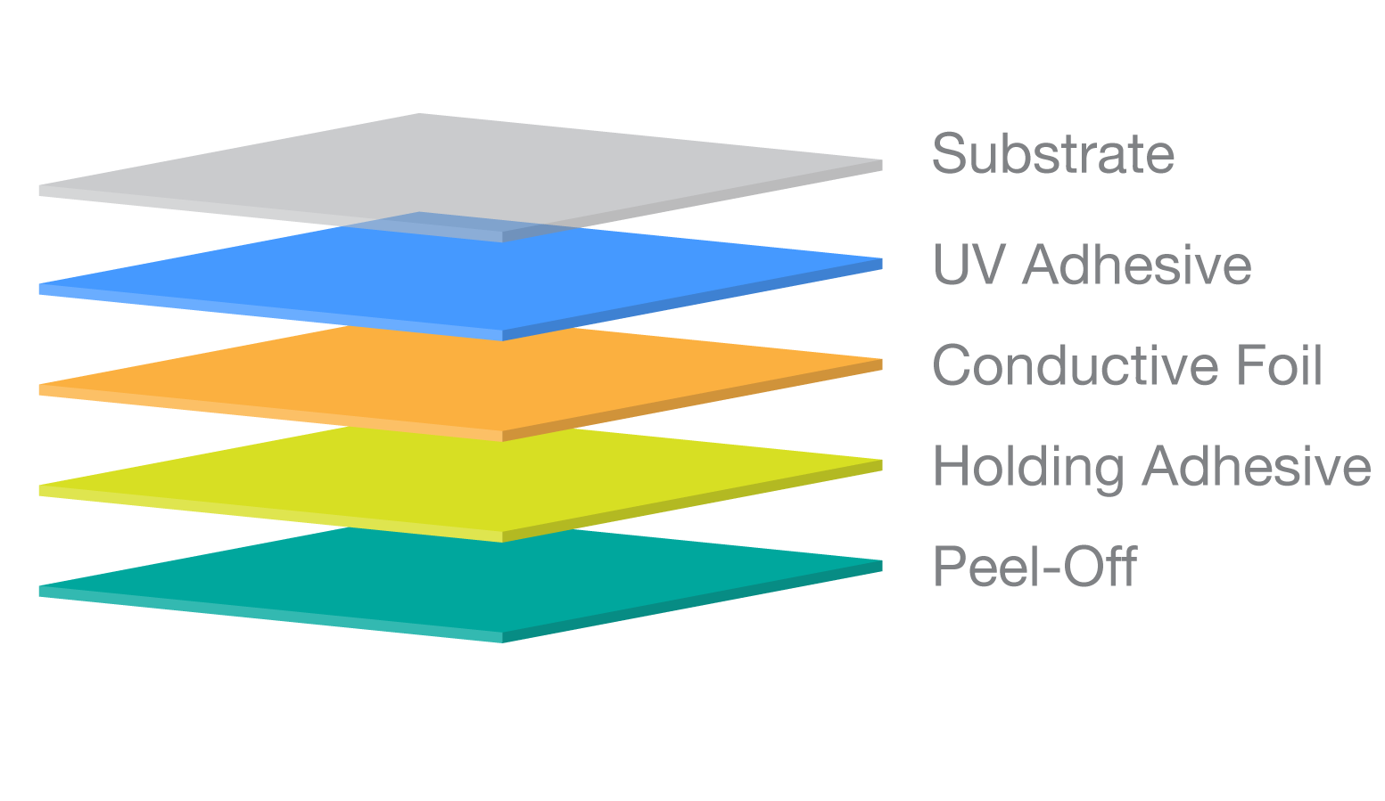
08/22/2016 at 23:52 • 0 commentsThe Printem Film is a self contained film that contains all the materials necessary for the creation of a copper PCB. In the current version, the Printem Film has 5 layers as show below
This is a brief description of the stack, for more detailed look, please wait for more project logs or you can also read the full paper here
![]()
1) The substrate is made of Acetate paper, the kind you use to print slides on for old style overhead projects, this is what the PCB will be finally formed on ( currently working on using a high temperature resistant alternative )
2) Then we coat this substrate with a UV curing adhesive, these adhesives basically bond and activate when exposed to UV light, this is the active component of the Printem Film
3) Then we have the conductive foil, in our case this is a copper foil bought from a crafts store, silver, gold and tin foils can also be used as long as they are thin enough, we are looking for a similar thickness as to the decorative gold foils you find in craft supplies
4) The holding adhesive basically holds the above layers to the peel off layer below . This has to be an adhesive that is strong enough to hold the stack together but weaker than the UV adhesive in its cured state ( More details to follow in the posts to come )
5) Finally the peel of layer is simple card sock that is thick enough to block light
All the layers above are arranged in the order as show and put through a roller press to bond them together into a single sheet. Once the sheet has been formed its ready for use. This seems like a lot of work to do. But the vision is that you will be able to buy sheets of Printem Film and use them without having to go through any of the above steps.
The next log will go into how all the above materials work together to create the final result.
-
Using Printem
08/22/2016 at 23:32 • 0 commentsThe goal of Printem is to let anyone easily, quickly and cheaply create Printed Circuit Boards for prototyping use. Imagine if one could create single layer, copper PCBs in less than 2mins after you design them, one will be able to quickly test and iterate on the designs, we believe that Printem is a useful tool for anyone who works with electronics and hardware.
So No Etching ! , No Special Inks !, No Special Equipment ! All you need is the Printem Film and a normal home office printer.
The build logs goes into how an end user would use Printem, this will be followed by posts on how the Printem film works, how to make your own and the current work that is being done on improving its various attributes. We would love to hear your thoughts on how useful Printem might be in your daily work.
![]()
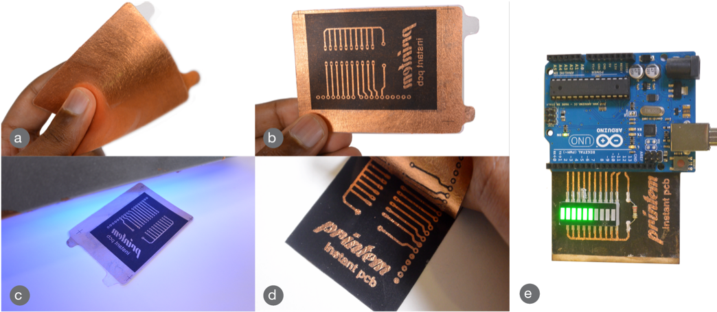
a) The key to Printem is the Printem Film - which i s a multilayer stack of materials that work together to produce the final copper PCB
b) The circuit pattern is printed on the Printem Film using any laser or inkjet printer using black ink
c) The film is then exposed to UV light or sunlight for 30 seconds ( or lesser if the light is intense )
d) The top layer is peeled off , revealing the copper PCB underneath, this is ready to use
e) This just shows a simple LED bar graph being interfaced with an Arduino.
All this only takes about 2 mins !
Printem - Instant Printed Circuit Boards
A novelmulti-layer film that lets you quickly and easily make flexible copper PCBs all using normal, unmodified home printers
 varunperumal

