Form Factor
The main goal for the FunKey Zero project is to prototype the maximum number of features for our final #Keymu - open source keychain-sized gaming console machine. The keychain form factor is the most limiting parameter: roughly, we determined that 4 cm x 4 cm x 1.5 cm were the maximum allowed dimensions to stay practical, which leaves just enough room to fit a 1.5" screen, not much larger. This rules out event the small Raspberry Pi Compute module (67.6 mm x 30 mm) or Zero (65 mm x 30 mm) as the core processor board for the project.
Screen Resolution
With a lot of tricks, it is possible to stuff some emulators with a 128 x 128 pixel resolution on an ESP32, for example, like the small PocketSprite.
But based on our Edison Keymu experience, we determined that a 128 x 128 pixel resolution was barely acceptable to play some games with small fonts, so we tried to get a screen with a higher resolution, still fitting the 1.5" size.
If you search well, you can find on AliBaba some screen in this form factor with a resolution of 320 x 320 pixels but unfortunately, to handle the large amount of data to display, they use a high speed differential serial, user-unfriendly interface called MIPI DSI (Display Serial Interface) requiring a specific controller, only available in high-end mobile phone CPUs :-(.
We were lucky to find a nifty 240 x 240 pixel 1.5" screen with a simple SPI interface that is just perfect, which is now available at Adafruit.
RAM
However, a 240 x 240 pixel in 24-bit RGB color image takes a little bit more than 168 KB of RAM memory to store in a frame buffer, which is out of reach for most Micro-Controller Units (MCUs), except for the largest one.
Instead, we turned to bigger Central Processing Units (CPUs) with enough RAM memory, and if possible able to run a Linux OS in order to benefit from the existing software base, including already running game emulators.
But this extra RAM comes at a price: to reach these capacities, you need to use Dynamic RAM (DRAM) instead of the Static RAM (SRAM) used in MCUs. These are generally provided as external chips, with high-speed bus connections, requiring extra-careful PCB layout and trace routing, not counting for the required real estate on the board.
CPU with Integrated DRAM Memory
Considering the Raspberry Pi, for most models, this DRAM complexity problem was solved using a clever technique called Package on Package (PoP), which consists in soldering the DRAM package on top of the CPU itself.
Unfortunately, only a few chips outside the unreachable Broadcom CPUs used in the Raspberry Pi are using the same technique :-(
We found Next Thing Co.'s GR8 chip which combines a 1GHz Allwinner R8 ARMv7 Cortex-A8 processor with NEON SIMD extensions and a Mali-400 GPU. 256MB of DDR3 SDRAM in a single 14 mm x 14 mm x 0.8 mm package. Hopefully, we only found it too late, as Next Thing Co. is now dead, RIP.
Another option is the Octavo OSD335x-SM module which combines a 1GHz TI Sitara ARM Cortex-A8 AM335x processor and up to 1GB DDR3 memory into a slightly larger 21 mm x 21 mm x 3.08 mm package. This chip is used in the PocketBeagle. Sure, it contains almost all the required components, but it is about 1/4 of our total PCB area... More worrisome, this chip (like the GR8) is based on an older design ARM Cortex-A8, which has been superseded by the smaller, simpler and more power-efficient ARM Cortex-A7 in 2013. Be careful, the ARM version numbering is very confusing!
We then discovered the Allwinner V3s chip wich combines a 1.2GHz ARM Cortex-A7 with NEON SIMD and VFPv4 extensions and 64MB DDR2 memory into a user-friendly 16 mm x 16 mm x 1.6 mm (including pins) LQFP128 package. No more worries regarding the power consumption, but now some concern about the small DRAM memory size... (Note: in the meantime, Allwinner introduced the V3, which is the same CPU with 2x or 4x the amount of DRAM in a smaller 12 mm x 12 mm TFBGA package!).
Evaluation Board
In order to quickly evaluate the V3s performance in terms of power consumption and DRAM memory size, we wanted to get a ready-made evaluation board.
The only one we could find was the LicheePi Zero. We missed the Indigogo campaign by a few weeks, but we eventually got some boards in August 2017. Today, they are very difficult to get, the only place you can find them is on TaoBao for ¥47 (USD 7.40), you need to select "zero核心板" ("Zero Core board"). But ordering on TaoBao is quite an experience, good luck!
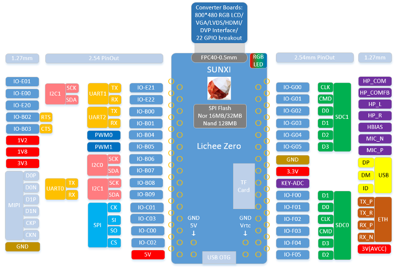
This board features the AllWinner V3s chip we need and exposes most pins on a convenient dual pitch (1.27 mm and 2.54 mm) rows of holes on the board edges, so that you can both mount through-hole headers to use on a breadboard, or solder it on a main PCB as an SMT module.
The LicheePi Zero module can be powered either from its built-in Micro-USB OTG connector, or using its +5V pin. We do not want to use the micro-USB, as we want to be able to insert an automatic switch known as an "ideal diode" to disconnect the +3.7V LiPo battery when operating from the USB +5V power supply, and there is no way to do this on the board. Hopefully, the USB data signals USB_DP and USB_DN are both routed to the board edge pins, so we can use an external micro USB connector:

It is not documented in this pinout, but there is indeed a RESET castellated pin on the right side of the USB OTG connector.
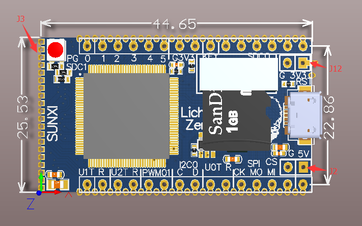
The LicheePi Zero module contains an SD/TF Card holder (simple one, no push-pull type), and the only modification we had to perform was to desolder the 3 resistors near the RGB LED at the top right corner of the board, as they interfere with some of our GPIO usage. We do not use at all the top FPC40 connector.
As you can see, almost all V3s pins are broken out to module pads, either on a 2.54 mm or 1.27 mm pitch.
Controlling on the V3s datasheet, this module almost perfectly matches our needs:
- 12x GPIOs with interrupt capabilities for the buttons (U/D/L/R and A/B/X/Y pads, rear L & R buttons, plus START and SELECT buttons)
- 1x Analog audio output to play on a speaker (using an external audio amplifier chip) or on headphones using an audio jack
- 1x RESET button
- 1x USB device interface to mount as a memory device on a host
- 1x UART for console debug
- and of course, 1x SPI bus plus some extra GPIOs (LCD_RESET, RS and PWM for screen backlight) for the LCD screen!
There is even a spare I2C bus that can be convenient to control some external Power Management IC (PMIC) in our #Keymu - open source keychain-sized gaming console!
The LicheePi Zero module form factor is a little bit too large for our #Keymu - open source keychain-sized gaming console, but still very close:

In the #Funkey Zero, we turn the module 90° CW and used it as an SMT module, which requires a "U" slot on the main PCB as the LicheePi zero features components on both sides of the PCB. Given the central LCD position with keypads on both sides, this almost fixed the overall shape and dimensions of the design.
 Squonk42
Discussions
Become a Hackaday.io Member
Create an account to leave a comment. Already have an account? Log In.
cool
Are you sure? yes | no
Very nice write-up, thanks. So the Keymu will have a custom PCB with this chip? Do you have a source of the chips?
Are you sure? yes | no
Yes, we are currently designing a CPU module featuring the AllWinner V3s chip, the AXP203 PMIC and a micro SD Card slot in the Edison form factor (35 mm x 25 mm x 3.9 mm) using the same kind of Hirose DF40 Series “header” connector (less pins, though), as this connector comes in several convenient mating heights. It will be a 4-layer PCB.
Given our final dimensions (~ 40 mm x 40 mm x 15 mm) for the Keymu, we found that stacking PCBs was the best way to pack everything into the small enclosure and leave enough space for the battery, like we did for Keymu v1 with the Edison.
It is now quite easy to find V3s and AXP203 chips on AliExpress or AliBaba: https://www.aliexpress.com/item/sku/32836406274.html
I actually already have some pieces on my desk!
Are you sure? yes | no