Close
0%
0%

RC2016/99: TI-99/4A clone using TMS99105 CPU

Retrochallenge 2016/10 entry and winner: try to build a TI-99/4A clone using a TMS99105 CPU and an FPGA. In a month...

Similar projects worth following
The retrochallenge 2016/10 is the first retrochallenge competition that I participated. The "competition" lasted for a month and is described here: http://retrochallenge.org

I set myself a pretty ambitious goal of building an enhanced TI-99/4A home computer from scratch. TI made many compromises and unusual design decisions when building the machine. It was the 1st 16-bit home computer, but did not quite deliver a higher performance than the 8-bit home micros of the time.

For a long time I have wondered what the machine might have been if some of those compromises did not have to be taken, or if the computer was updated using TI's best parts of the era.

I surprised myself and managed to build my TI-99/4A clone in a mont, using the limited free time I had. This project is one of three winners of the RC2016/10 competition.

Link to EP994A files at Github

Fastest TI in the world?

I believe I now have the world's fastest TI-99/4A compatible computer, running at 7 times the speed of the original while using a CPU from 1982, the time when the original TI-99/4A was available.

Old and new happily together

I wanted to combine old and new components, to have that retro aspect. For the "old" part I used the TMS99105 CPU from 1982. This was the fastest processor of the TMS99 range from TI, so a good basis for an enhanced TI-99/4A. For the "new" part I went with a Xilinx Spartan 6 series field programmable logic array (FPGA), to build the rest of the computer apart from the CPU. I wired the "new" and "old" parts together.

Best part of the project: TI 99er community

When I started the project I was looking forward to completing some pieces of a TI-99/4A compatible system. I did not expect to finish the project with something as complete I have now. I did expect to get some feelings of accomplishment as I was confident I could get some parts of the design working. While it was great to have the sense of accomplishment many times over the course of the project (getting the CPU to run, video hardware drawing a screen, Basic booting, games running) that was completely overshadowed by the support I got from the community. So a big thank you to everyone for your comments, advice and encouragement.

The result at the end of October

The project logs below describe the various steps I took to build the project, but as a summary these are the components I developed over the course of the project:

  • TMS99105 "testbed" on a protoboard, basically I plugged in the CPU chip and a couple of components like the clock oscillator to the protoboard to see if the CPU worked. And it did work!
  • Wiring up the FPGA: the next order of business was to connect the CPU protoboard to a FPGA board. I used the Saanlima Electronics Pepino development board for thais purpose. So a bunch of wires went between the protoboard and the FPGA board.
  • Memory interface: I built a memory interface in the FPGA chip, allowing the TMS99105 to communicate with the memory on the FPGA board.
  • Memory loader: I took an existing design of mine, which combines a VHDL component running on the FPGA and a PC host program communicating with the FPGA, allowing me to load software from PC to the memory of the TMS99105.
  • TMS9918 video processor implementation on the FPGA. This is not 100% complete, but it has support for graphic modes 1 and 2, sprites and scan doubling to allow displaying the video output on a VGA screen.
  • TMS9919 sound chip in VHDL. This took less time than I expected and is not completely tested, but I have 3 sound channels and a noise channel so the core features of the chip are there.
  • Keyboard emulation: the FPGA implements a portion of the functionality of the TMS9901 I/O chip which is used (among other things) on the original TI to communicate with the keyboard. In my case I use a PC keyboard and a serial channel to communicate the button presses to the FPGA, which presents the keyboard codes via the TMS9901 functionality to software in manner compatible with the original TI.
  • Support for banked ROM and GROM, to allow running of TI Basic, TI extended Basic, most games and other software.

Starting point - the beginning of October

This is what I initially wrote about my retro challenge project, in the beginning of October:

Back in the day TI used the TMS9900 CPU for the TI-99/4A home computer. That CPU choice was made due to schedule pressure and led to some strange design choices. TI followed up the TMS9900 family with two other generations of TMS99 family CPUs before the family became extinct: the TMS9995 and the (most powerful) TMS99000 series. My understanding is that no-one has yet tried to build a clone with the TMS99000 series CPU, so I will try to do that with a TMS99105 chip in October 2016 as my retro challenge entry.

Building something like this in a month with very limited spare time is going to be a challenge, to...

Read more »

tms99105rev2.pdf

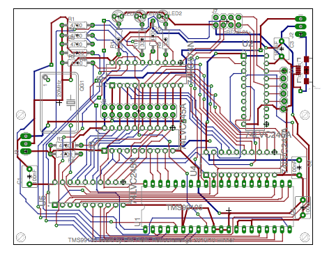
PCB Design sent to manufacturing.

Adobe Portable Document Format - 71.39 kB - 12/08/2016 at 07:34

Preview

tms99105rev2-schema.pdf

New version of the schematic, corresponds to the PCB.

Adobe Portable Document Format - 28.10 kB - 12/08/2016 at 07:34

Preview

  • 1 × TMS99105 16-bit microprocessor in 40 pin DIL package
  • 1 × 74LVC245 Logic ICs / Receivers, Transceivers
  • 1 × Clock oscillator 20MHz 14 pin DIL for factor, 4 pins
  • 6 × 4.7k resistor
  • 3 × 100nF capacitors Power decoupling

View all 7 components

  • Running MEGADEMO on the TMS99105!

    Erik Piehl09/28/2018 at 20:01 1 comment

    I spent a fair amount of time getting back to speed with the TMS99105 project. I have in the meantime advanced my own TMS9900 VHDL core. This sister project by now had a more compatible version of the TMS9918 video processor, and a little different memory map from the TMS99105 version.

    As a reminder: In principle my two projects are almost identical, running on the same Pepino FPGA board, the only major exception being that the first version of the TI-99/4A clone uses the TMS99105 physical CPU chip on an external daughterboard, while my latter project is the same, but replaces the TMS99105 chip with my own version of the TMS9900 core, thus integrating it to the FPGA. As I have been working on this project more lately, it has gotten more advanced.

    Nearly all of the VHDL files are identical between the two projects, the obvious differences being a different top-level module, integrating either the TMS99105 external CPU or the TMS9900 core as a VHDL module.

    Enough of background - the difference that prevented me from running the Megademo on the TMS99105 system was that this version had an older version of the memory map, and did not support a "ROM" cartridge of 512K which is a requirement for the Megademo. To be more precise the Megademo comes in different versions, but the one of interest to me is the one that requires 512K of paged ROM space - and I provided that in the latter project by rearranging how the 1MB external memory of the Pepino board was divided between different functions.

    I ran into great difficulty in simply copying the same memory layout over from the TMS9900 core system. After some intense head scratching I determined that the seeming insignificant memory map change resulted consistently in timing problems, making the TMS99105 system very unstable. For now I solved this problem by just bypassing the memory paging unit, therefore limiting the addressable RAM to 32K, down from 256K of paged memory while simultaneously allowing for a 512K ROM area to exist. The ROM area is paged too, having 64 pages of 8K in size, but this paging mechanism is very simple compared to the RAM paging system. The RAM paging seems to be on the critical path.

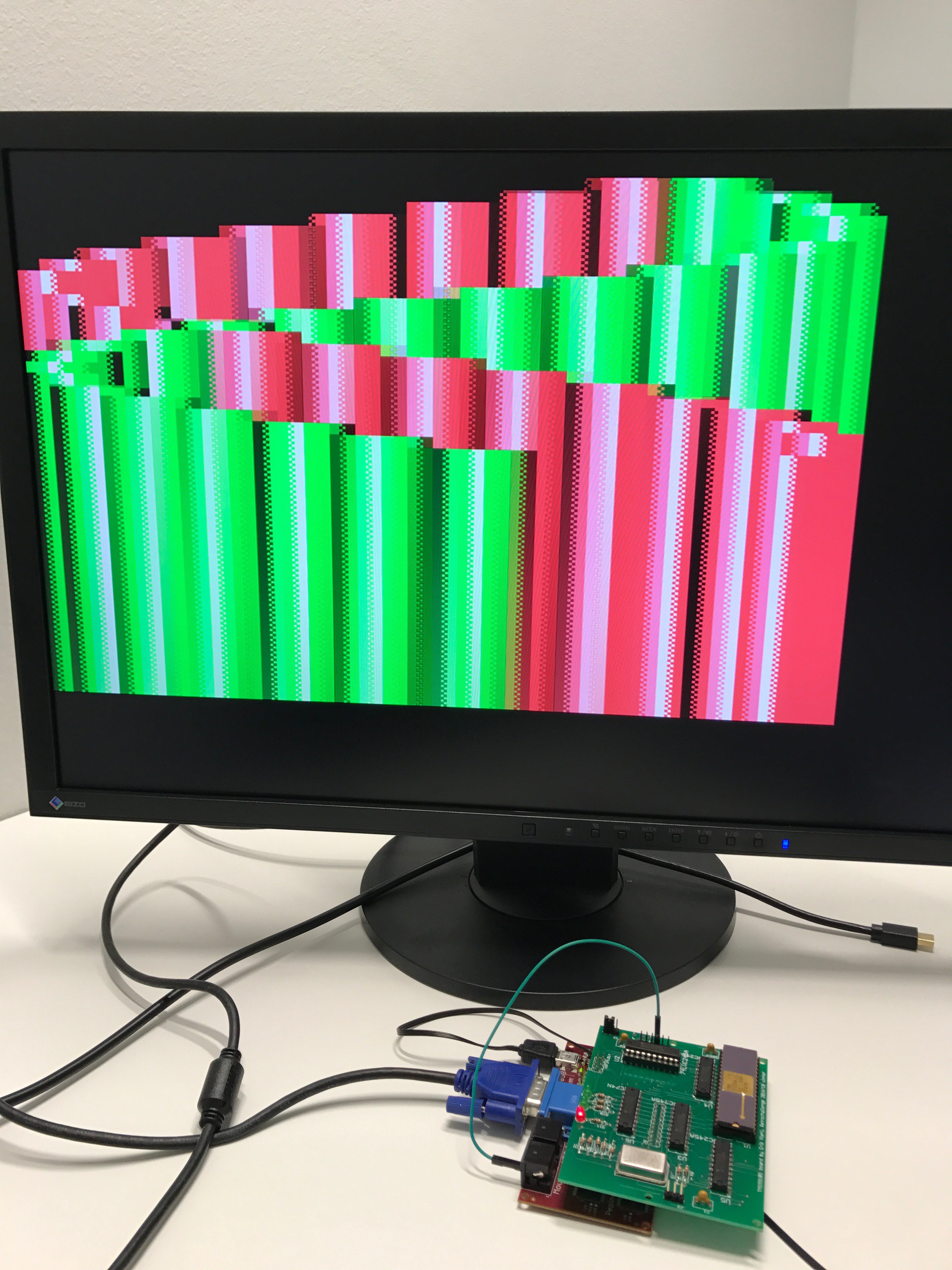
    To cut long story short, with 512K of ROM space I was able for the first time to run the Megademo with the TMS99105 CPU. On real TI CPU iron, with my FPGA implementation of the rest of the TI-99/4A. Needless to say, it runs very fast, having about 7x the processing power of the original TI-99/4A. The most interesting aspect of this test of running the demo for me was that the TMS99105 version has the exact same problems as shown when using my own processor core. Most of the demo runs just fine, but a couple demo sections still show graphics glitches and towards the end the demo gets stuck. This proves to me that my TMS9900 clone is now getting "very" compatible, and that most likely the problems I am encountering now in the demo are due to 1) my TMS9918 video processor clone still having compatibility issues and 2) the place of the demo where execution gets stuck is likely due to poor implementation of some TI-99/4A feature used by the demo but not relating to graphics (smells like TMS9901 timer interrupt to me).

  • Information about successor project

    Erik Piehl10/03/2017 at 07:43 0 comments

    I recently noticed that my TMS99105 project at hack-a-day has more followers than my successor project to this one, so I thought I will just provide here a quick link to that project. I understand that some people may be interested in the TMS99105 project in it's own right, and I really like this project too, it came well out. 

    After "completing" this project to a functional state I've worked on my VHDL implementation of the TMS9900 core, allowing the entire TI-99/4A to be re-created in the FPGA. That design is largely compatible with this one, all the peripherals like the TMS9918 and TMS9919 are the same in both projects. The source code to both projects is in the same repository,  with the TMS9900 VHDL implementation being in the "soft-cpu" branch.

    Successor project reference

    I may still make updates to this project too, as I really like the shiny TMS99105, and also because it is currently still more tested than the successor project. So as I make updates to the peripherals etc I will probably bring those improvements over to this project too.

  • Small update to TMS9918: 5th sprite on scanline flag

    Erik Piehl04/01/2017 at 03:58 0 comments

    After a while a quick update: I found at AtariAge a really cool demo for the TI-99/4A, using scanline effects.

    Link to AtariAge

    Unfortunately that did not work on my TMS99105+FPGA system, as my TMS9918 VHDL model did not support detecting 5 or more sprite per scanline condition. That's now fixed, and the demo runs :)

  • Circuit boards work

    Erik Piehl01/14/2017 at 05:30 0 comments

    It's been a while since my last update. During the time I haven't had that much time to put into the project. However, there is some nice progress:

    I have fully assembled two boards and they work. As can be seen from the picture above, one extra wire is still needed to carry the CPU's write signal to the FPGA. All the other signals are delivered through the pin headers. The two headers carry a limited number of signals: the larger header has 16 signal pins. These are used in a three way multiplexing scheme, timing is based on the CPUs address latch signal. These are the phases:

    1. Address transfer from CPU to FPGA (early part of the address latch high). This part takes about 30 nanoseconds.
    2. Control signal transfer from FPGA to CPU and sampling of some CPU signals from the CPU to the FPGA. This takes the next 30 nanoseconds.
      1. The 16 data signals are treated as two groups of eight during this part of the cycle
      2. One group is from FPGA to CPU, in practice the FPGA clocks 8 signals to the 74ACT574 flop flops. These signals include CPU reset, interrupt, non-maskable interrupt, and other control signals, including the input for the green LEDs. One of the LEDs is simply toggled when 2^19 clocks of address latch are received and allows us to see that the CPU is running. The other LED is lit when the disk subsystem is active.
      3. The other 8 signal group is used to sample the status of some control lines of the CPU by the FPGA. A 74LVC245 buffer is driven active to do this. The signals include BST1, BST2, BST3, #MEM and #WR. The last one of these, #WR, appears so late in the cycle that I added the red wire depicted above to be able to continuously sample it, instead of trying to sample it during this control signal transfer window.
    3. Data transfer either to the CPU (reads) or from the CPU (writes). Writes are simply sampled a few 100MHz clock samples into the cycle when #WR has gone low. For reads the FPGA needs to present the CPU with the data for as long it samples it. That is the reason why the #RD signal is not among the multiplexed control signals but rather available directly to FPGA via the other header, which carries 6 control signals in total. Only two signals from the CPU are directly available via this header: #RD and ALATCH. The remaining 4 signals are control signals driven by the FPGA to control the various buffers and the aforementioned 74ACT574 latch. This part of the cycle takes the remaining 140 nanoseconds or so (a memory cycle is 200ns at 20MHz).

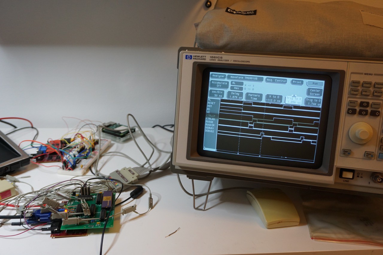
    This timing sequence is somewhat visible in the logic analyser picture below:

    In the picture there are a few notable signals:

    • AL shows the CPU's address latch signal and is the basis of timing
    • CTRLCP is the clock driving the 8-bit 74ACT574 register. The FPGA generates this signal once it has sampled the address over during AL high (the sampling occurs over the 16 signal pins).
    • CTRLRD enables a 74LVC245 buffer so that the FPGA can read the bus status lines. Active low.
    • BUSOE, when low, allows the FPGA to observe or drive the 16-bit multiplexed address/data bus of the CPU.

    As can be seen in picture, BUSOE and CTRLRD are effectively the same signal, the other is just an inverted version as the 16 signal bus can only either be used for control signals or the address/data bus. CTRLRD is active for 30 nanoseconds. The rising edge of CTRLCP appears 20 ns into this cycle, to provide enough time for the buffers to settle.

  • PCBs arrived from manufacturing

    Erik Piehl12/20/2016 at 07:55 0 comments

    It is always a great feeling to get the physical boards from manufacturing :)

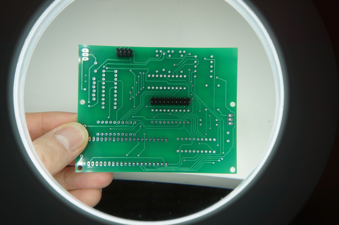
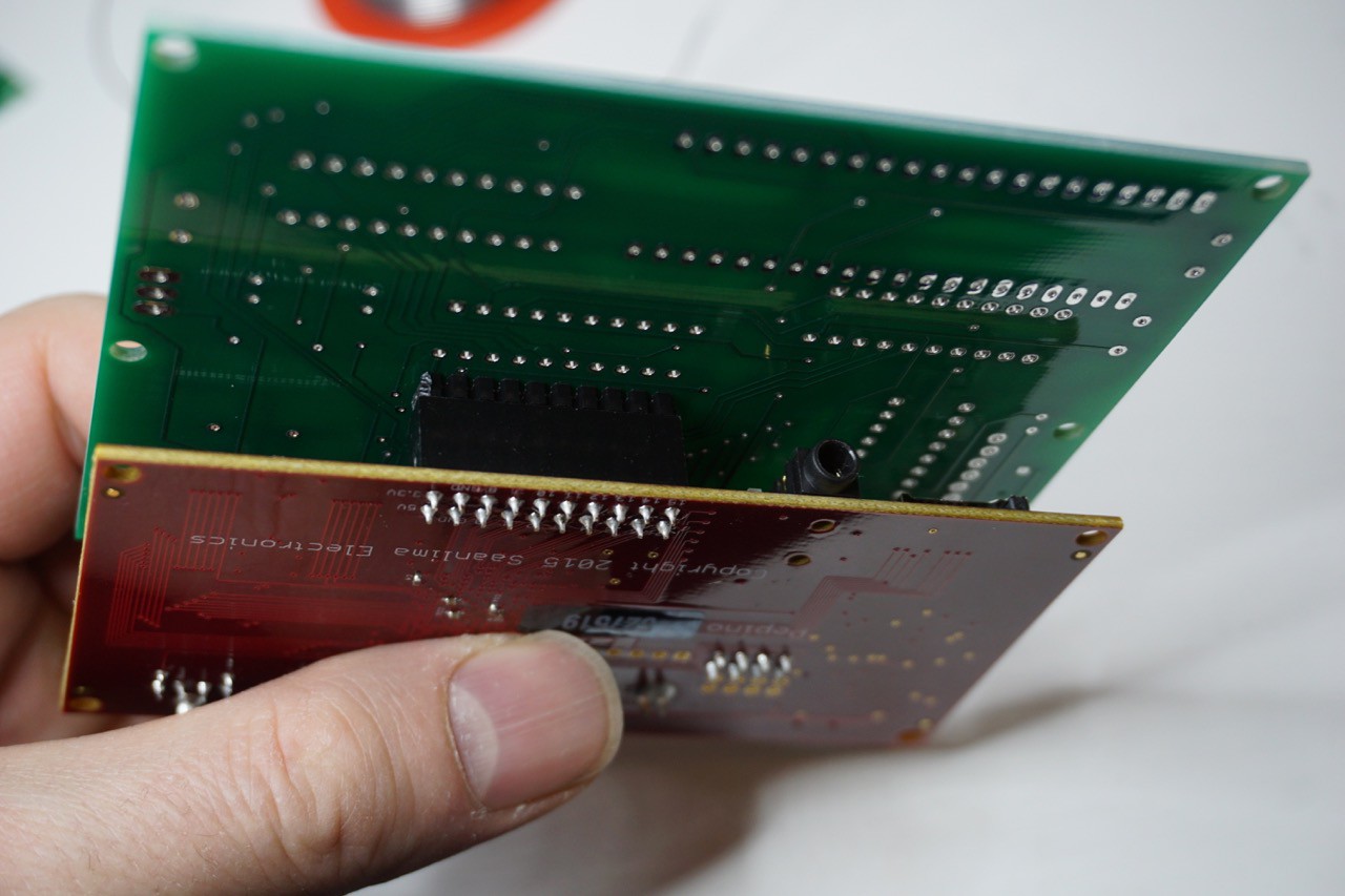
    I had no real time to check the boards, but on the surface they seem fine. At least the connector measurements turned out ok and the board perfectly connects to the Pepino FPGA board.

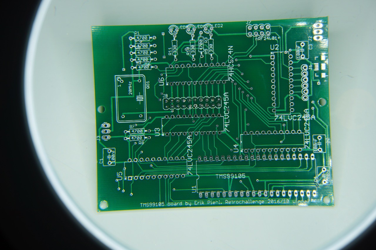
    The top of the board, photo taken through my magnifying glass / light:

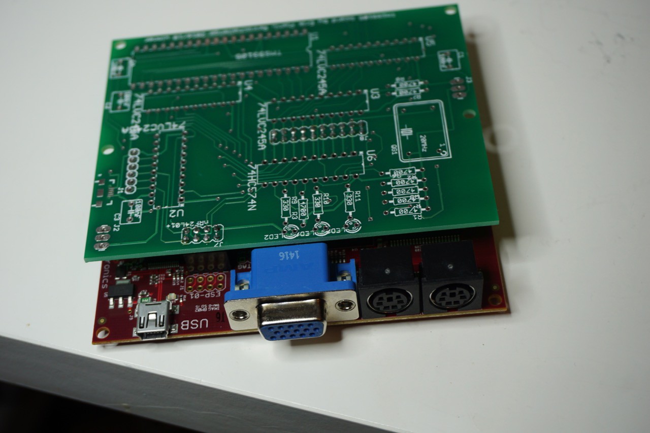
    Bottom side, with connectors mounted (no time yet for anything else):

    A close up of the connection to the Pepino, it appears the SD card and audio jack are still accessible:

  • Sticky graphics mode 2 bug fixed

    Erik Piehl12/15/2016 at 21:24 0 comments

    I have trying to understand why in graphics mode 2 the last character cell was showing bogus information and finally understood the problem. It was on the hardware side, the character address was incremented too early, and the VHDL code was using the new value although it should still have used the old value. This has to do how character cells are treated in graphics mode 2: in this mode the screen supports 768 unique character values, but they are specified in a funny way. The screen is divided into 3 vertical bands of 256 characters, in each band the 8-bit character values are re-used.

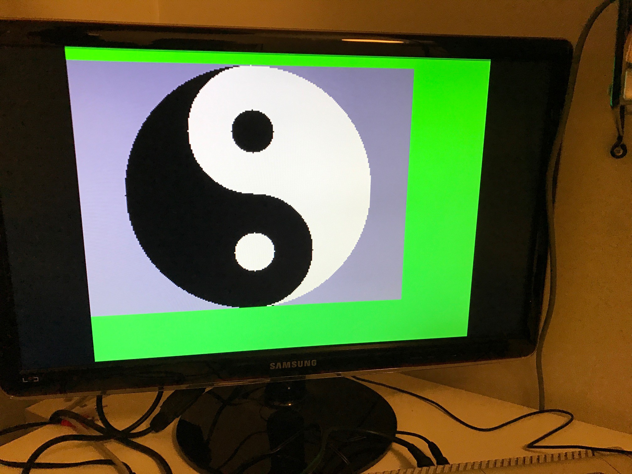
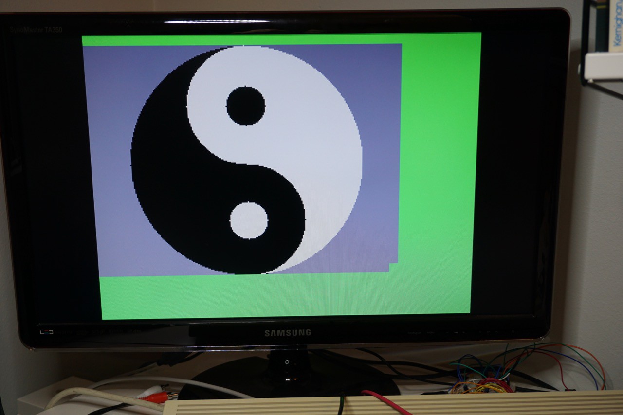
    My problem was that the increment for the very last character cell happened too early, causing that particular character to roll over to a non-existing "fourth set" of 256 characters. The same problem probably also caused problems for the last characters of the bands 0 and 1 too. Anyway, now it is fixed and Yin/Yang displays in all its glory without bugs - this bug actually was visible in the Parsec too - but not anymore. Updated code in GitHub.

  • PCB design sent to manufacturing

    Erik Piehl12/08/2016 at 07:40 0 comments

    I have spent some hours designing a printed circuit board for this design. This will be a board that plugs in on top of the Pepino board. I did this on purpose using only through-hole components just in case there are people interested in building one of these. Personally I prefer SMD components, and that would have allowed the board to be somewhat smaller.

    I also revised the schematics, to be able to support the entire TMS99105 feature set. That required some more signals. Since I'm already using all the pins available on the Pepino board, I put in a couple more buffers and a latch to store control signals. That will meant that the already multiplexed address/data bus will have another phase (under FPGA control) to read the additional CPU output signals (such as BST1, BST2 and BST3) and to latch control signals to the latch.

  • Sprite bugs fixed

    Erik Piehl11/30/2016 at 18:54 0 comments

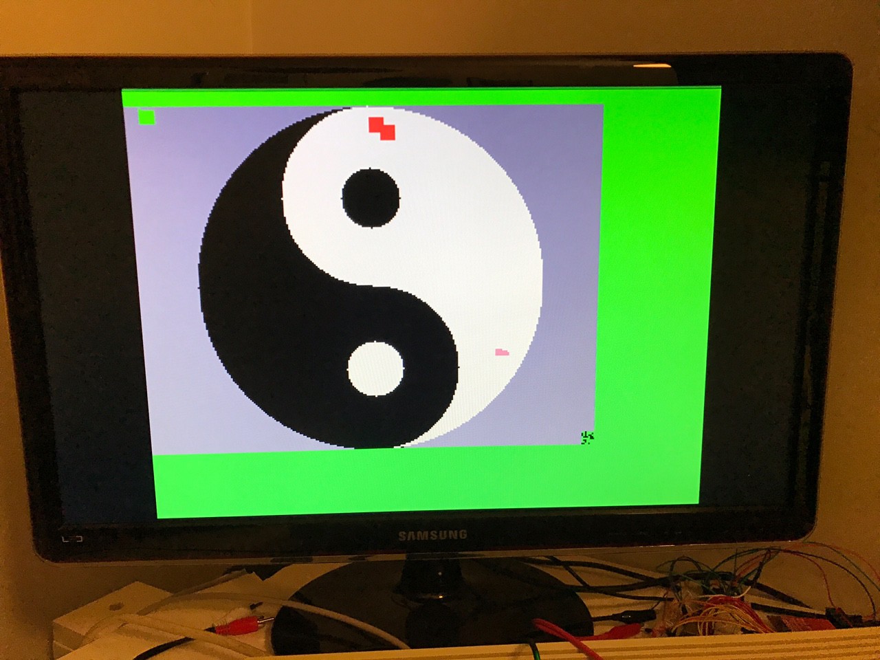
    I did a small update, now the sprite bug should be gone, although that did reveal another potential bug as can be seen in the picture below: the lower right hand corner has a missing block for whatever reason... But at least there are no red sprites in there.

    While fixing the VDP, I also added a few more extra read only registers. These are 16-bit registers available in the address space of the CPU. Mostly they are there for convenience to have direct VDP memory pointers, VGA scanning registers actually allow changing of VDP memory synchronised to the scan.

    AddressComments
    8880High byte returns contents of VDP register 0 (low byte zero)
    8882High byte returns contents of VDP register 1 (low byte zero)
    8884Pattern memory pointer in VDP memory (based on reg 2)
    8886Color table pointer in VDP memory (based on reg 3)
    8888Character table base address in VDP memory (based on reg 4)
    888ASprite attribute table base in VDP memory (based on reg 5)
    888CSprite pattern table base in VDP memory (based on reg 6)
    888EHigh byte returns contents of VDP reg 7 (colours), low byte zero
    8890Current value of VDP memory pointer
    8892VGACol - current VGA scan column
    8894VGARow - current VGA scan row
    8896MSB: line buffer bank (toggles between 0 and 1, VGA refresh hardware reads from linebuffer indicated by this bit).
    LSB: 1=when display blanking active
    Bits 14..1: 0 when read

  • First successful assembler run

    Erik Piehl11/28/2016 at 19:47 0 comments

    I've been working rather slowly on the disk subsystem support. After fixing numerous bugs and my own misunderstandings, I was finally able to run TI's original Editor/Assembler software system on the TI-99/4A clone.

    Getting editor assembler to work is an interesting milestone due to the way the cartridge works: actually the cartridge is a GROM only cartridge, so it does not contain any machine code software, just GPL code. It loads the machine code assembler from the disk (the files ASSM1 and ASSM2). These two files are loaded as binary programs. When assembling, the source coded is loaded from the disk as variable length record file, while assembler output (the object file in TI's tagged hex annotation) is written as a fixed record file.

    To run the assembled program, the disk subsystem also needs to be able to load a fixed length record file. Thus overall there is a fair amount of different types of files that the disk subsystem needs to work with. I used Matthew Hagerty's nice Yin/Yang assembler program as a test. The output can be seen below, complete with bogus sprites. The sprites are there due to hardware bug I have in the sprite engine design, I guess it starts to be time to fix it... Basically the sprite engine does not properly recognize when to stop drawing sprites.

  • File access starts to work a bit

    Erik Piehl11/25/2016 at 09:37 0 comments

    I posted to youtube a new video showing the system running RXB 2015. I haven't had much time work on the design, but the little time I had I've been working on the disk support subsystem. Most of that code runs on the PC, and communicates with the system over USB. I'm starting to understand how the TI-99/4A disk system works.

    In addition I remapped the memory of the FPGA system, so that the paged memory extension on the TI-99/4A clone now has access to 512K of RAM, up from the previous 256K.

    I guess I need to try the game more on the classic99 emulator as I don't know if the game runs properly... At the end of video I got stuck... Sorry the video is pretty boring as I did not have time to work on it either. During loading you can see the sprite bugs in the top left hand corner - my VDP implementation still doesn't properly process the "no more sprites" code (vertical coordinate set to >D0), so it will spit out extra sprites. Sprite size doubling is not supported by the hardware, as can be seen from the size of the loading text.

    From a technical point of view to get this far the system requires support for SAMS memory and the following disk subsystem opcodes: load, open, read, close. While they seem trivial, they are not exactly that. I went ahead and blatantly copied a bit of code from classic99 (the file buffering code)...

View all 29 project logs

Enjoy this project?

Share

Discussions

John Odum wrote 11/06/2021 at 18:23 point

Hi, I just found this project and it sounds amazing.  (These are the sort of things I wonder about myself -- what could have been?)  Are there any recent updates on this project?

  Are you sure? yes | no

lezanderson wrote 03/09/2017 at 11:54 point

What an Amazing project...Cool..!

  Are you sure? yes | no

Barry Nelson wrote 10/26/2016 at 13:00 point

Is it possible to slow the system down to the speed of a classic TI99/4A?

  Are you sure? yes | no

Erik Piehl wrote 10/27/2016 at 06:25 point

For background, the goal of this design was not to make a cycle-exact copy of the TI. Instead I was looking if I could use the most advanced version of the TMS99 family as a CPU to make the system go fast.

There are a number of ways to slow the system down to speeds that are close to the original TI-99/4A, although not exactly the same. The TMS99105 has a minimum clock frequency of 12MHz, so we could begin by doing that, it would roughly half the speed of the system, although it still would be much faster than the 99/4A. Additional slowdown could be created with wait states (requiring an extra wire from the FPGA to the CPU to control its "Ready" signal) or by having the FPGA create extra interrupts and making a change to the system ROM to just waste time in those extra interrupts. Either way the resulting speed could be made very close to the original TI-99/4A, but not exactly the same.

Erik

  Are you sure? yes | no

Ralph wrote 10/17/2016 at 22:37 point

if i remember correctly the 9900  was removed and a socket installed then a wire wrapped 

daugter  board instsalled this project was between toronto 9t9 userer group and don o'neil of wht  ps have you check stuart conners web site http://www.stuartconner.me.uk/

  Are you sure? yes | no

Erik Piehl wrote 10/18/2016 at 06:07 point

Ok that makes sense. Yes, the site of Stuart is great and one of the inspirations for me to start working on the TI again in the first place. I have exchanged some e-mails with him too, he has always been very supportive.

  Are you sure? yes | no

Ralph wrote 10/16/2016 at 22:10 point

i do not think it was documented probably mid 90s past proto

i'm getting old but i did the hard wiring on the project

  Are you sure? yes | no

Erik Piehl wrote 10/17/2016 at 15:37 point

So that was already some time ago then - interesting. Did I understand properly that you wired this internally? Basically the idea being that it would replace the TMS9900?

  Are you sure? yes | no

Ralph wrote 10/06/2016 at 22:42 point

a number of years ago  we started an accelerator project using this cpu in a ti 99 4/a started the clock slow and speeded it slowly replaced as many buffers as possibile with fast chips as all worked great then we smoked everything the hardware at the time was not designed for the speed of the cpu

  Are you sure? yes | no

Erik Piehl wrote 10/07/2016 at 12:27 point

Interesting! When was this and is it documented anywhere? What I am doing is quite different, as there is no real TI-99/4A hardware involved, instead I am trying to keep things simple in terms of number of chips, and make things complex only inside the FPGA. Thanks for your comment!

Cheers, Erik

  Are you sure? yes | no

Erik Piehl wrote 09/28/2016 at 07:25 point

Hi Bob, that's interesting. There are people in the retro computing that would be interested in that material (including me). Thanks for the comment and good luck for the search :)

Cheers, Erik

  Are you sure? yes | no

bsheff2 wrote 09/27/2016 at 21:33 point

Hi, back in the '80s I was involved with a company building a TMS 990 vertical application for Legal offices.   Somewhere I have the source for a small system, assembler, terminal word processor, C compiler and UCSD Pascal.   Found some, looking for rest.

regards, Bob

  Are you sure? yes | no

Erik Piehl wrote 09/28/2016 at 08:00 point

Hi Bob, that's interesting. There are people in the retro computing that would be interested in that material (including me). Thanks for the comment and good luck for the search :)

Cheers, Erik

  Are you sure? yes | no

Similar Projects

Does this project spark your interest?

Become a member to follow this project and never miss any updates