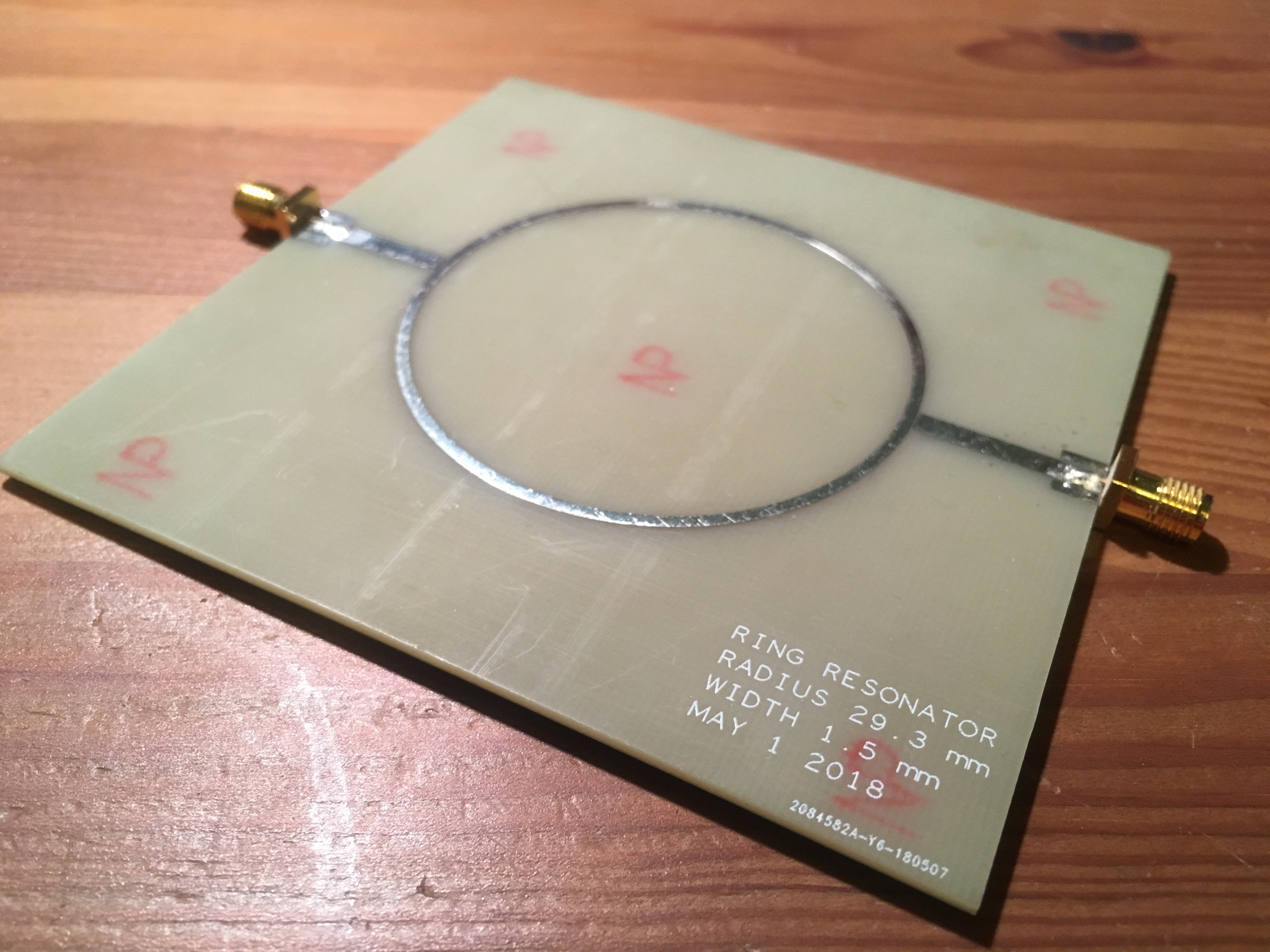
Here is an assembled resonator. Nice to only have to solder on a couple SMAs rather than a whole bunch of components and be able to get to measuring right away.
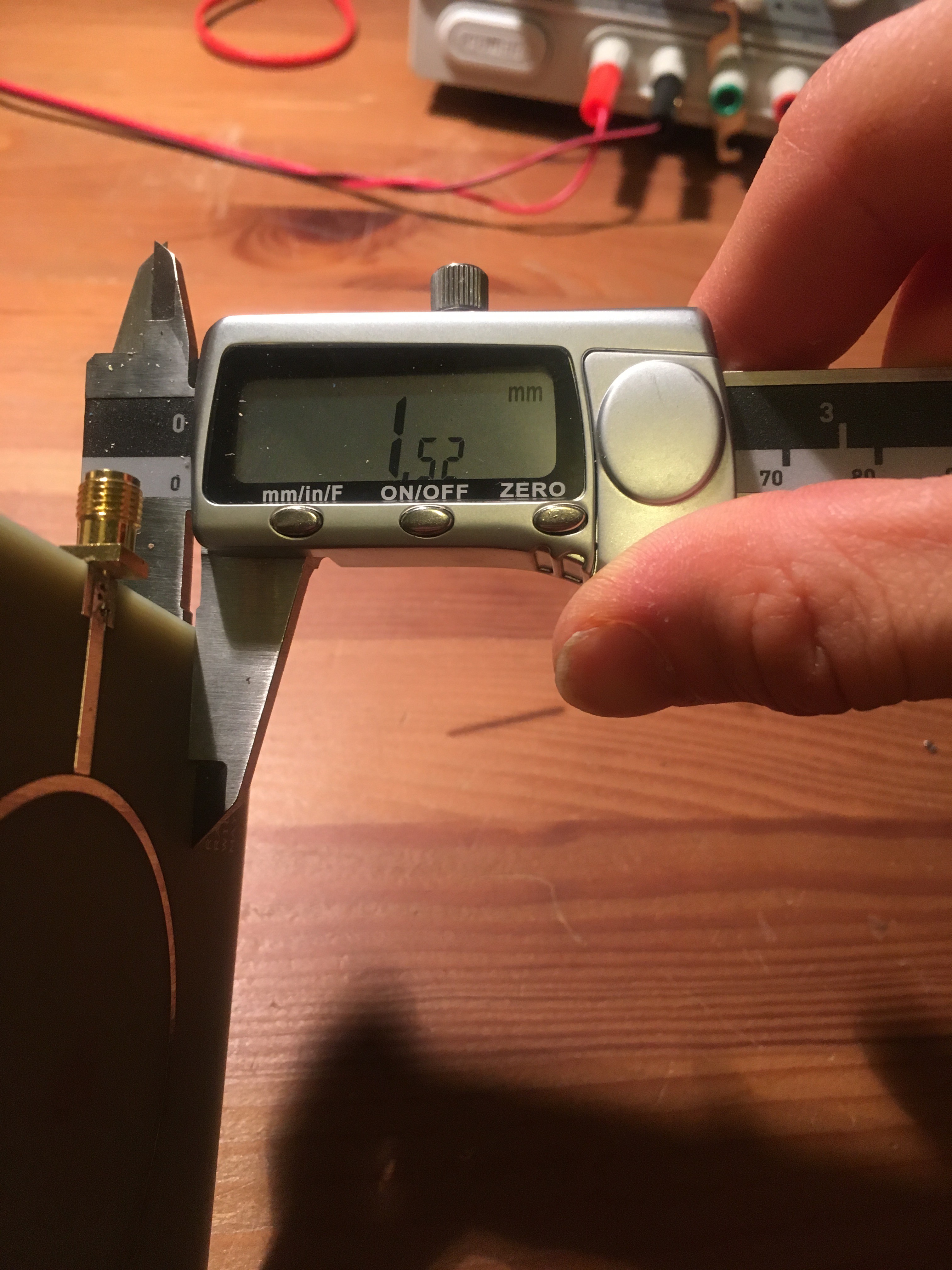
Based on my calculations, for a 1.6 mm PCB with 1 oz. copper (0.0175 mm layer), the substrate should be 1.565 mm thick. When I measured with a calliper, the thickness came in at 1.52 mm, which includes the bottom copper pour. So I used a thickness of 1.51 mm in the calculations.
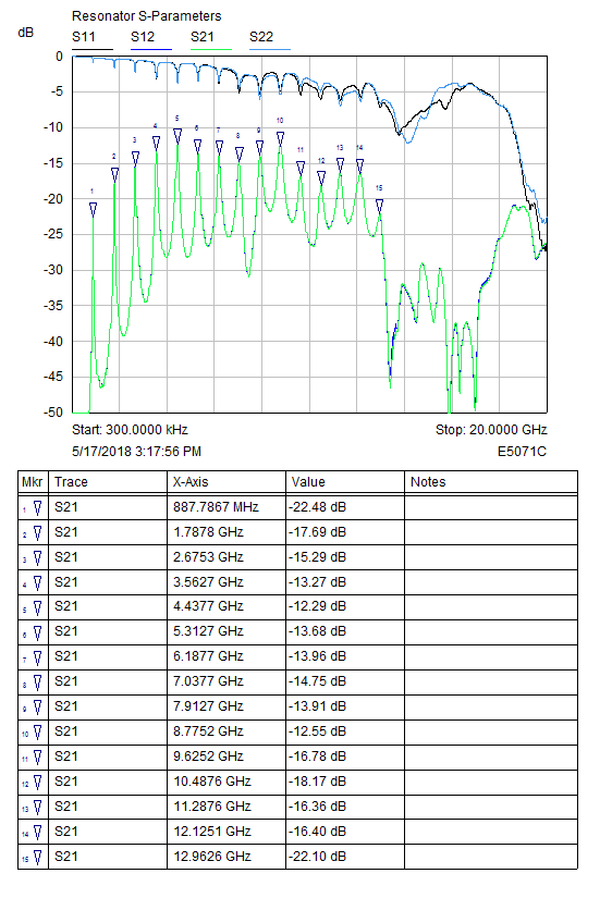
The VNA I used to measure the resonators went up to 20 GHz, but the shape of the graph started to go wonky after about 13 GHz. I suppose some other phenomenon starts to show up after that. This still gives me 15 points at which to calculate the dielectric constant.
I updated the MATLAB script to take an array of the frequencies where there are minimums of S21 (the resonant frequencies) and plot of graph of the relative permittivity over frequency. Here is what I got:
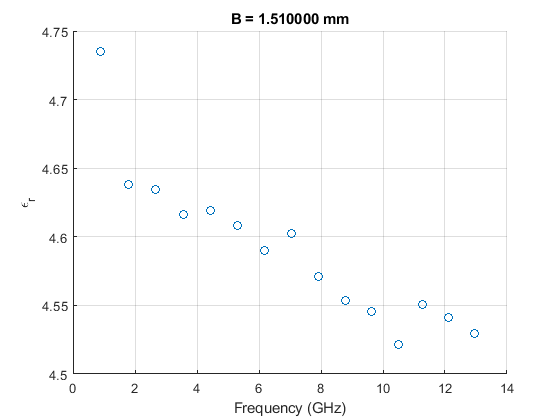
The trend of decreasing εᵣ over frequency is consistent with the graph towards the end of this article. Also, the permittivity is greater than 4.4 that I have been nominally using in my calculations.
Discussions
Become a Hackaday.io Member
Create an account to leave a comment. Already have an account? Log In.
Can you calculate the loss tangent from this data as well? Have an example calculation and results for your data? I've tried asking JLCPCB for a datasheet for their FR-4, but they couldn't answer me, your investigation is probably the most accurate source for this info, I also have access to a VNA and would like to repeat your experiment for a few of their stackups/PCB heights.
Are you sure? yes | no