-
Front Panel Deposit Operation
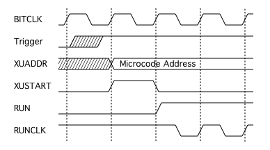
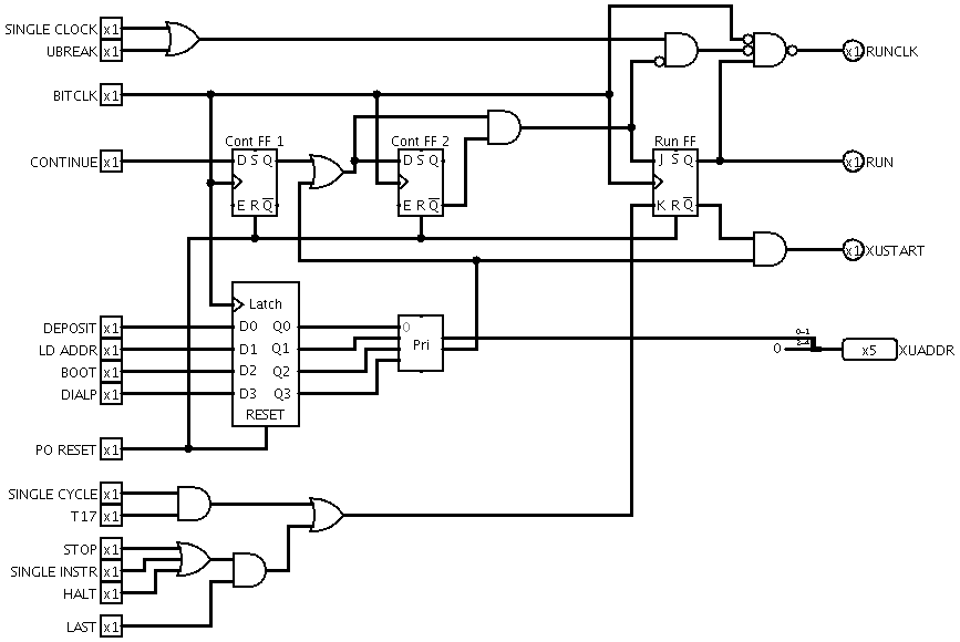
07/26/2020 at 07:17 • 0 commentsThe Run Control subcircuit now has provision for initiating up to four different non-instruction microcode sequences (NIMS). The inputs for triggering these are first latched to synchronise them with BITCLK, and then fed to a priority encoder which generates a microcode address. At the same time, the Continue FF chain is activated, producing a one-BITCLK pulse at XUSTART and then setting the Run FF.
NIMS Timing
![]()
Run Control
![]()
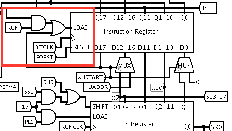
Instruction Register Loading
I found a problem with the logic for loading the NIMS entry point address into the instruction register. It doesn't work if the instruction register is clocked with RUNCLK, because the XUSTART pulse occurs before RUNCLK is activated. So the instuction register is now continuously clocked with BITCLK, and functions that should only occur while the machine is running are gated with RUN.
![]()
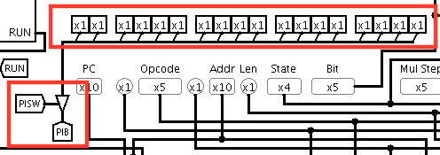
Input Switches and Parallel Input Bus
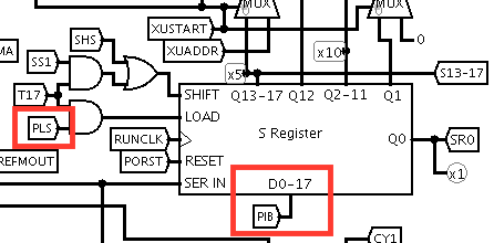
I added a set of switches for manual data entry1. These are gated onto a Parallel Input Bus (PIB) which connects to new parallel inputs on the S register.
![]()
![]() There is currently only one data source for the PIB, but there will be others later. I needed a way of selecting the PIB source in the microcode, but there are no more bits available, so I have re-used part of the UBADDR field. This means I won't be able to perform a microcode branch and use the PIB at the same time, but I don't think that will be a problem.
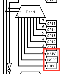
There is currently only one data source for the PIB, but there will be others later. I needed a way of selecting the PIB source in the microcode, but there are no more bits available, so I have re-used part of the UBADDR field. This means I won't be able to perform a microcode branch and use the PIB at the same time, but I don't think that will be a problem. ![]() The function of the Deposit switch will be to write the value from the input switches into memory at the address currently in the PC, and then increment the PC. To do this, I need to be able to select the PC as the source for the memory address, and increment the PC, independently of other functions.
The function of the Deposit switch will be to write the value from the input switches into memory at the address currently in the PC, and then increment the PC. To do this, I need to be able to select the PC as the source for the memory address, and increment the PC, independently of other functions.![]()
![]()
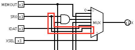
I also need to be able to select the serial output of the S register as an X source in the ALU input selector.
![]()
Deposit microcode
# XSEL values
XSR  = 011  # S Register

# MISC values
PLS   = 1110  # Parallel load S register
LDPC  = 0001  # Load PC from IR
INCPC = 1001  # Increment PC
MAPC  = 0101  # Memory address = PC

# Deposit
   1 00000 0 0000 :  -   -   --  ---   -  --    -     -   --   -   -   -   -   -    -   PLS     -   ---    PISW -- # Load switches into S
   1 00000 0 0001 : SHS  -   --  XSR   -  --    -    WMEM --   -   -   -   -   -    -   MAPC    -   ---    ----    # Write S to memory
   1 00000 0 0010 :  -   -   --  ---   -  --    -     -   --   -   -   -   -   -    -   INCPC   -   ---    ----    # Increment PC
   1 00000 0 0011 :  -  EOI  --  ---   -  --    -     -   --   -   -   -   -   -    -   HALT    -   ---    ----    # Stop
Footnotes
1. This is not quite historically accurate. The EDSAC designers deliberately did not provide a way for users to enter programs manually, because they didn't want people taking up machine time debugging at the console. It did have a set of "engineering switches" that were used for maintenance, but I don't know exactly what they did or how they were used.
-
Non-Instruction Microcode
07/25/2020 at 11:23 • 1 commentTo progress further, I want the ability to initiate microcode sequences by means other than executing instructions. The main purpose for this is bootstrapping, but I also have some other uses in mind, such as implementing the telephone dial interface. I would also like to have a way of manually depositing data in the memory for diagnostic purposes.
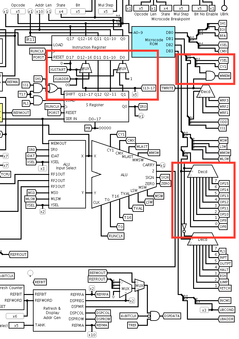
To make way for these extra microcode sequences I have added a bit to the microcode address, and a corresponding extra bit to the instruction register. I have also inserted a multiplexer between the S-register and the instruction register to allow a microcode address to be introduced from an external source, to be determined later.
I'll also need to be able to encode more microcode operations, so I changed the bit assignments a little. I don't really need the CYP carry control value (carry from previous ALU operation) because it can be derived from LSW, so I removed it and reduced the carry control field to one bit. Then I moved the WMEM bit to where CYP previously was, freeing up a bit to expand the MISC field to four bits. This gives me another 8 MISC values to play with.Changes to top level
![]() By the way, if you're wondering why the Main Memory and Microcode ROM are now coloured, it's so I can find them easily for loading data into them.
By the way, if you're wondering why the Main Memory and Microcode ROM are now coloured, it's so I can find them easily for loading data into them.
-
Tidying Up
07/23/2020 at 09:18 • 0 commentsThe top-level schematic was getting a bit cluttered, so I moved some of the logic into subcircuits.
- Main memory address multiplexing
- Register file address multiplexing -- incorporated into the RF Address Incrementer subcircuit
- Bit address multiplexing -- incorporated into the Bit Counter subcircuit
- ALU input selection
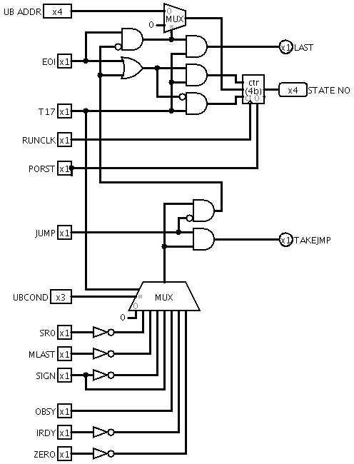
- Microcode branching -- combined with the State Counter and renamed to State Control
Also, the latches before the inputs to the ALU have been moved back into the register file subcircuit. This uses more latches, but has the advantage that the signals going to the ALU input selection network are stable instead of flipping between CPU and display refresh values, which makes troubleshooting easier.
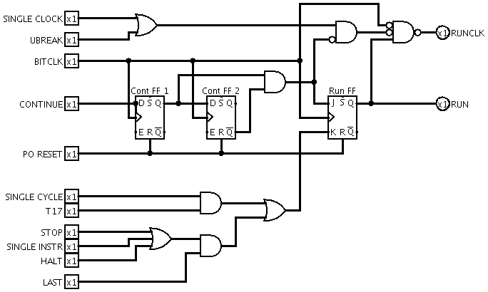
Change to Run Control
While tidying up, I managed to break the Halt instruction, and this led me to discover a drawback in my implementation of Single Clock mode. The way I had it, when in Single Clock mode, the Run FF was set for one BITCLK cycle and then cleared. However, this made it difficult to debug the Halt instruction by stepping in Single Clock mode, because I couldn't distinguish between then Run FF being cleared by the Halt instruction and by the Single Clock mechanism.
So I modified the Run Control subcircuit slightly. Instead of feeding into the Stop logic, the Single Clock mode input now simply freezes RUNCLK in the same way that UBREAK does. The Run FF remains set, and a single RUNCLK pulse is allowed through each time CONTINUE is pressed.
As part of this change, the gate for enabling RUNCLK has been moved from the top level into Run Control.Updated Schematics
Top Level
![]()
Run Control
![]()
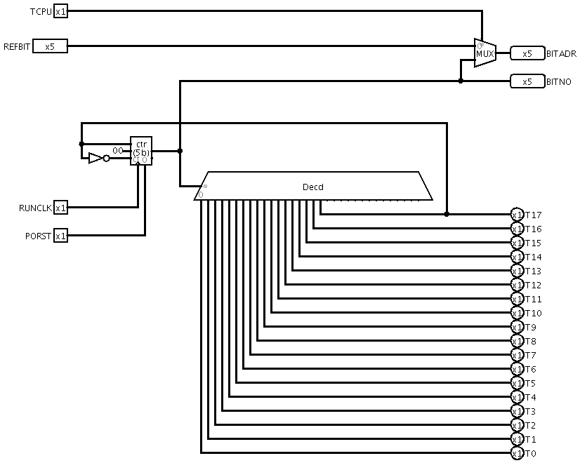
Bit Counter
![]()
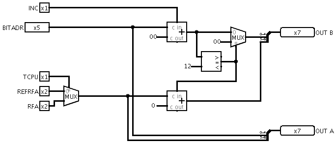
Register File Address Generator (formerly Register File Address Incrementer)
![]()
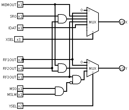
ALU Input Select
![]()
State Control (formerly State Counter)
![]()
-
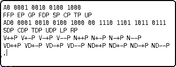
Combined Test Program
07/20/2020 at 11:07 • 0 commentsI have finished the combined test program.
Expected output:
![]()
The strategy is:
- Test the Output instruction by printing the name of the next test ("A").
- Test the short Add instruction, and print the contents of the accumulator using a minimum of other instructions. The result is designed to give an easily recognisable bit pattern.
- Test all the jump instructions. The name of each test is printed followed by "P" for pass or "F" for fail.
- Test the short Subtract instruction using Add and Jump If Not Zero to verify the result.
- Test most of the other short word instructions. Subtract can now be used to verify the results.
- Test the long Add instruction and other long word instructions using a similar strategy.
- Test the multiplication instructions for various combinations of operand signs.
If any test fails, the program prints "F" and halts at that point. When all tests pass, "." is printed at the end.
-
Fixing bit 17, more properlyish
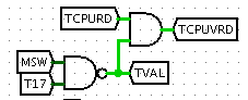
07/19/2020 at 08:01 • 0 commentsI had to undo the last change to the ALU, because it broke things.
The ALU, and also the right-shifting mechanism, need to work on full 18-bit words with the sign bit in bit 17, to accommodate a one-bit overflow of intermediate results during multiplication. As long as the final results of arithmetic operations don't overflow, bits 16 and 17 should be the same, but there are ways for them to become different, which can lead to the Zero FF being set incorrectly.
To fix this, I did two things:
1. In the ALU, the Zero FF is not updated during bit 17.
2. Bit 17 is forced to be the same as bit 16 when reading an operand from memory. This is done by a transparent latch after the output of the RAM that is frozen during bit 17 of an MSW. (A separate output is taken directly from the RAM for display refresh, so that the actual memory contents can be seen).
Two new timing signals are derived for these purposes, TVAL (Valid Bit) and TCPUVRD (Valid Bit during CPU Read cycle).
![]() New ALU subcircuit:
New ALU subcircuit:
![]() New main memory subcircuit:
New main memory subcircuit:
![]()
-
More Jump Instructions
07/10/2020 at 12:26 • 0 commentsI found while writing the test program that programming with just the two original EDSAC jump instructions was quite awkward, so I added a couple of instructions from a later version of the machine: an unconditional jump, and a jump if AC nonzero.
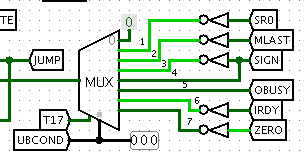
To support the jump if nonzero instruction, I connected my one remaining ubranch multiplexer input to the zero FF output from the ALU. (I hope I won't need any more ubranch conditions!)
Both of the new jump instructions are encoded with opcode F, and distinguished by instruction bit 0. Accordingly, they are written in assembly language asF addr F # Jump
F addr D # Jump if nonzero
(In the original version of the EDSAC, opcode F was "Read the last character output for verification". I don't think I will miss that.)
New ubranch input:
![]()
Microcode for the new jump instructions:# UBCOND values BNZER = 111 # Zero FF = 0 # F F - Unconditional jump 10001 0 0001 : - EOI 11 X0 - Y0 CY0 -- - - MSW LSW - - - JUMP - BSGN0 ---- # F D - Jump if accumulator <> 0 10001 1 0001 : - - 00 XAC - Y0 CY0 -- - - - LSW - - - --- - --- ---- 10001 1 0010 : - - 10 XAC - Y0 CY0 -- - - - - - - - --- - --- ---- 10001 1 0011 : - - 01 XAC - Y0 CY0 -- - - - - - - - --- - --- ---- 10001 1 0100 : - EOI 11 XAC - Y0 CY0 -- - - MSW - - - - JUMP - BNZER ----
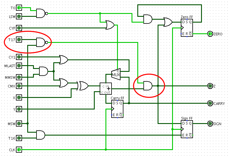
ALU Change
While testing the Jump if Nonzero instruction, I found that I had to add logic to the ALU to force the unused bit to zero so that it would not spuriously set the Zero FF.
![]()
-
Assembler
07/10/2020 at 12:22 • 0 commentsI wanted to write a combined test program to exercise all the instructions, so I can tell whether I've broken something when I make a change. It quickly became apparent that writing any sizeable program with the tools I had so far would be a very tedious exercise.
So, I wrote an assembler. Yes, this is cheating slightly, since the builders of the original EDSAC had no such luxury available, but I figure I've already served my time doing hand assembly during my 8-bit era, and I want to finish this project some time during my life.
Here's a sample program:# # Hello World # A i_out F # Initialise the Output instruction T out F A msg_len F # Initialise the char counter T count F loop: A count F # Decrement the char counter A k_m1 F G stop F # End of the message? T count F out: O F # This instruction is modified to address succcessive chars A out F # Increment the address in the Output instruction A k_2 F T out F F loop F # Go back for next char stop: Z F # Finished i_out: O msg F # Initial value of Output instruction k_m1: -1 F # Constants k_2: 2 F count: 0 F # Char counter msg_len: 12 F # Length of message msg: 'aHELLO WORLD' # Message to print ('a' is Letters Shift) -
Display Troubleshooting
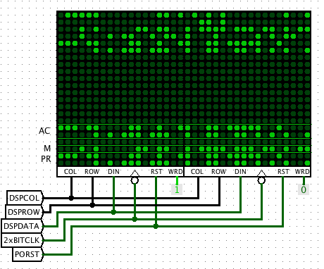
12/20/2018 at 11:55 • 0 commentsSpeeding up the display
I found that my display emulation circuit was slowing down the simulation by a factor of 4, so I replaced it with a multiplexed design. I changed the "Input Format" of the LED Matrix components to "Select Rows/Colums" and eliminated the flip-flops from the panel driver circuit. With 864 fewer flip flops, the simulation now runs only 50% slower than it did before I added the display.
The panel driver now simply provides row/column select signals for the LED matrices:
![]()
I also removed the flip-flop that was holding a value for the display data input line and replaced it with a gate that pulses the input during the second half of each refresh cycle. With the "Light Persistence" parameter of the LED matrices set to 3500 ticks (slightly longer than a complete display refresh) this produces a stable display.
![]()
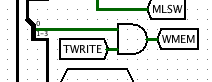
Memory Write Glitches
I found that spurious changes were occurring to the memory contents since I added the display. I fixed this by gating WMEM with TWRITE, so that memory writes only occur during the CPU Write phase. The previous gating of WMEM with RUNCLK was removed.
New gating:
![]() New main memory subcircuit:
New main memory subcircuit:
![]()
-
Memory Refresh and Scope Display
11/25/2018 at 00:55 • 0 commentsI've now implemented all the important instructions (I'm not going to bother with the Verify instruction, because it seems fairly useless), so it's time to move on to the dynamic memory refresh and oscilloscope display systems, which are closely related.
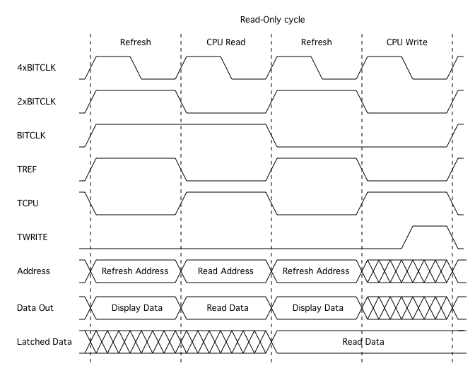
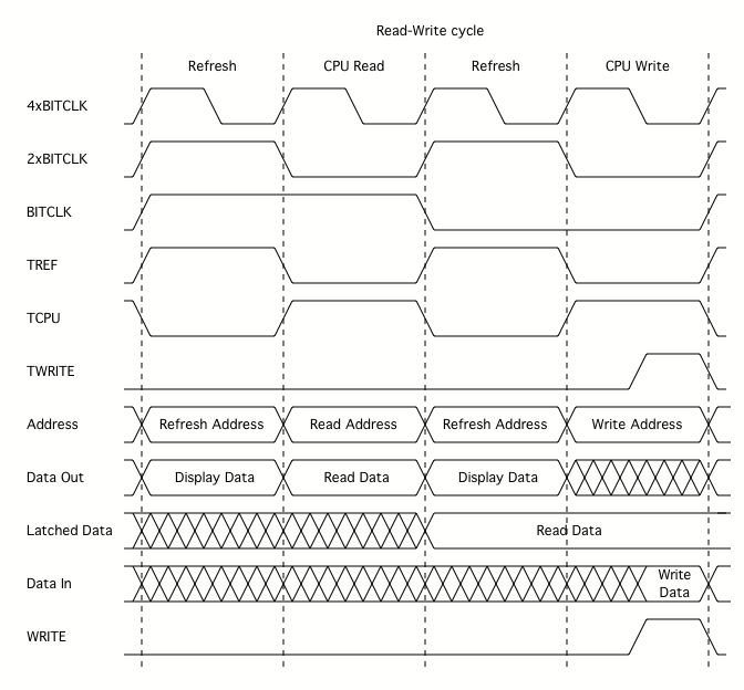
The plan is to divide each BITCLK cycle into four phases, of which two are refresh/display cycles, one is a CPU read cycle and one is a CPU write cycle. The following timing diagrams show what happens during one BITCLK period when the CPU performs a read-only cycle and a read-modify-write cycle.
![]()
![]() The required timing and address signals are generated by the Master Timing and Refresh Counter circuits. They contain a bit counter that counts from 0 to 17 and a word counter that counts from 0 to 43. The first 32 word counts address the main memory to refresh it and generate data for the display. The next 12 word counts are used to read display data from the register file.
The required timing and address signals are generated by the Master Timing and Refresh Counter circuits. They contain a bit counter that counts from 0 to 17 and a word counter that counts from 0 to 43. The first 32 word counts address the main memory to refresh it and generate data for the display. The next 12 word counts are used to read display data from the register file.
Master Timing:
![]() Refresh Counter:
Refresh Counter:
![]() The bit and word numbers from the refresh counter are rearranged and combined with a user-selected "tank" (memory page) number to produce addresses for the main memory and register files and control signals for the display. REFMA is the refresh address for the main memory. DSPREG selects one of the three register files and REFRFA selects a word from that file. DSPMR chooses whether to display data from the memory or the registers. DSPROW and DSPCOL indicate the row and column of the display for which data is being sent.
The bit and word numbers from the refresh counter are rearranged and combined with a user-selected "tank" (memory page) number to produce addresses for the main memory and register files and control signals for the display. REFMA is the refresh address for the main memory. DSPREG selects one of the three register files and REFRFA selects a word from that file. DSPMR chooses whether to display data from the memory or the registers. DSPROW and DSPCOL indicate the row and column of the display for which data is being sent.
![]() The purpose of this particular arrangement is to generate a display laid out as illustrated below.
The purpose of this particular arrangement is to generate a display laid out as illustrated below.
![]() These subcircuits are connected on the main circut as follows.
These subcircuits are connected on the main circut as follows.
![]() Multiplexers have been inserted into the memory and register file address lines to switch been refresh and CPU addresses, and some other minor changes made to ensure that things happen in the right phases of the BITCLK cycle.
Multiplexers have been inserted into the memory and register file address lines to switch been refresh and CPU addresses, and some other minor changes made to ensure that things happen in the right phases of the BITCLK cycle.
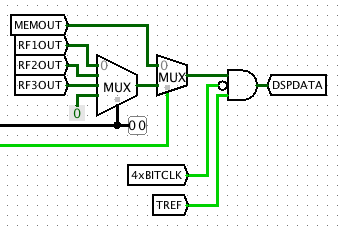
![]() I moved the latches on the outputs of the register files out of the register file subcircuit and put them before the X and Y ALU inputs, because I need the raw outputs from the registers to send to the display. Also, I realised that I don't need to gate the write input to the static RAMs with RUNCLK, because this is already done when generating TWRITE. The register file simulation subcircuit is now just:
I moved the latches on the outputs of the register files out of the register file subcircuit and put them before the X and Y ALU inputs, because I need the raw outputs from the registers to send to the display. Also, I realised that I don't need to gate the write input to the static RAMs with RUNCLK, because this is already done when generating TWRITE. The register file simulation subcircuit is now just:
![]()
Testing the display circuit in Logisim
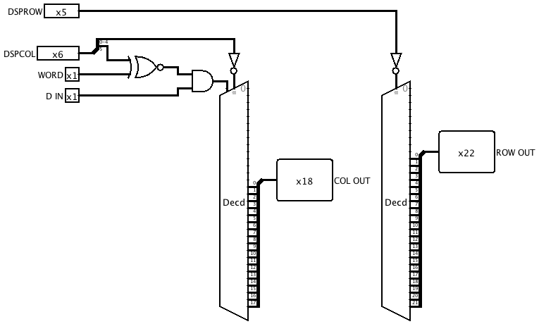
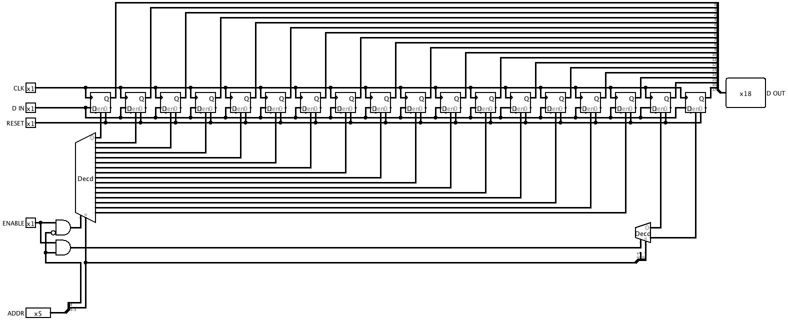
In the actual machine, DSPROW and DSPCOL will be used to generate X and Y scanning voltages for the oscilloscope, but Logisim doesn't simulate analog circuitry, so I put together a digital display using an LED Matrix component for testing purposes. I built a driver subcircuit consisting of 22 row drivers, each of which contains 18 individually addressable one-bit registers.
Row driver:
![]() I made the circuit symbol for the row driver one grid unit high, so that I could stack them up next to a decoder in the matrix driver (although this turned out not to help much, since I couldn't find a compact way to arrange the outputs).
I made the circuit symbol for the row driver one grid unit high, so that I could stack them up next to a decoder in the matrix driver (although this turned out not to help much, since I couldn't find a compact way to arrange the outputs).
![]() I designed the circuit symbol for the matrix driver to sit behind the LED matrix and provide a backdrop for it, as well as allowing two 18-wide matrices to be positioned side by side to form a 36 bit wide display.
I designed the circuit symbol for the matrix driver to sit behind the LED matrix and provide a backdrop for it, as well as allowing two 18-wide matrices to be positioned side by side to form a 36 bit wide display.
![]() It took a bit of fiddling to get this to work properly, because the order in which Logisim draws overlapping components on a schematic seems to vary randomly depending on exactly how things are positioned, and to make things worse, it changes every time the circuit is reloaded from a file. But when the planets are aligned, it looks pretty good.
It took a bit of fiddling to get this to work properly, because the order in which Logisim draws overlapping components on a schematic seems to vary randomly depending on exactly how things are positioned, and to make things worse, it changes every time the circuit is reloaded from a file. But when the planets are aligned, it looks pretty good.
![]()
-
Input Instruction
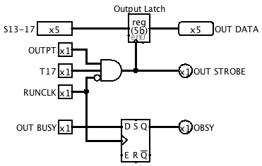
11/18/2018 at 22:29 • 0 commentsOutput Hardware Modification
I made a small change to the output interface. I realised it was probably a bad idea to connect the OBSY signal from the output device directly to the ubranch multiplexer, because glitches could occur if it changes near a clock edge, so I added a flip-flop to synchronise it with the bit clock.
![]()
![]()
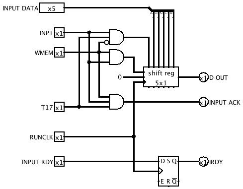
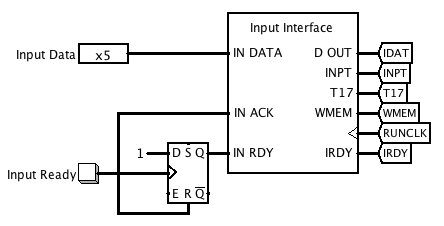
Input Hardware
The Input instruction reads a character from an input device (originally a paper tape reader) and stores it in the lower 5 bits of a memory location. To support this, I designed the following input interface. It consists of a 5-bit parallel-in serial-out shift register, and some logic to manage a pair of handshaking signals. INPUT RDY is asserted by the input device when there is data present, and INPUT ACK is pulsed by the CPU once the data has been accepted. The device is then expected to remove INPUT RDY and start reading the next character.
![]()
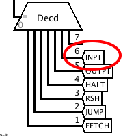
Reading the input data is a two-step process: first the data is loaded into the input register in parallel, then it is shifted out serially and written to memory. Rather than use up two MISC values for this, I allocated one MISC value called INPT and used WMEM to distinguish between loading and shifting. This effectively gives me two control signals for the price of one.
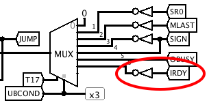
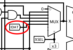
The INPUT RDY signal is synchronised with RUNCLK to produce IRDY, which is connected to an input of the microcode branch multiplexer. The serial output from the input register is connected to an input of the X multiplexer.
For testing purposes, I connected INPUT RDY to a flip-flop that emulates the handshaking action of an input device.
![]()
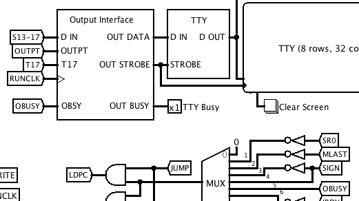
Other changes to the main circuit:
![]()
![]()
![]()
Input Microcode
INPT  = 011  # Load/shift input register depending on WMEM

BIBSY = 011  # Input data not available

# I - Input
   01000 0 0001 :  -   -   --  ---   -  --    --   --   -   -   -   -   -    -    -   ---     -   BIBSY  1000    # Loop until input data available
   01000 0 0010 :  -   -   --  ---   -  --    --   --   -   -   -   -   -    -    -   INPT    -   ---    ----    # Load data into input register
   01000 0 0011 :  -  EOI  --  XIN   -  --    --   --   -   -   -   -   -    -   WMEM INPT    -   ---    ----    # Write input register to memory
 There is currently only one data source for the PIB, but there will be others later. I needed a way of selecting the PIB source in the microcode, but there are no more bits available, so I have re-used part of the UBADDR field. This means I won't be able to perform a microcode branch and use the PIB at the same time, but I don't think that will be a problem.
 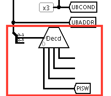 The function of the Deposit switch will be to write the value from the input switches into memory at the address currently in the PC, and then increment the PC. To do this, I need to be able to select the PC as the source for the memory address, and increment the PC, independently of other functions.
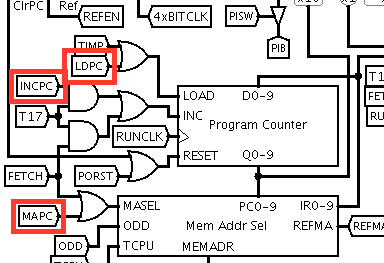
 By the way, if you're wondering why the Main Memory and Microcode ROM are now coloured, it's so I can find them easily for loading data into them.
 New ALU subcircuit:
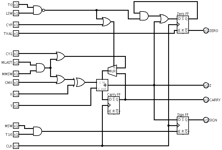 New main memory subcircuit:
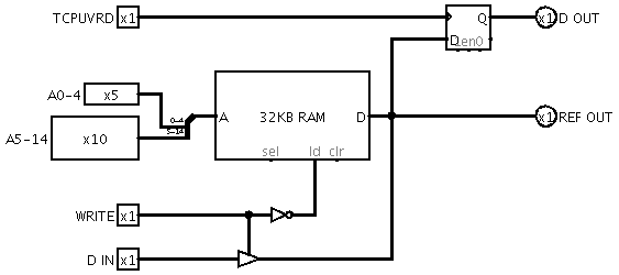
 New main memory subcircuit:
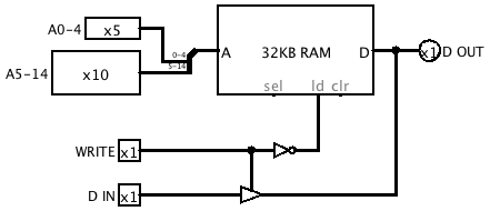
 The required timing and address signals are generated by the Master Timing and Refresh Counter circuits. They contain a bit counter that counts from 0 to 17 and a word counter that counts from 0 to 43. The first 32 word counts address the main memory to refresh it and generate data for the display. The next 12 word counts are used to read display data from the register file.
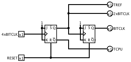 Refresh Counter:
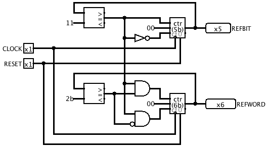 The bit and word numbers from the refresh counter are rearranged and combined with a user-selected "tank" (memory page) number to produce addresses for the main memory and register files and control signals for the display. REFMA is the refresh address for the main memory. DSPREG selects one of the three register files and REFRFA selects a word from that file. DSPMR chooses whether to display data from the memory or the registers. DSPROW and DSPCOL indicate the row and column of the display for which data is being sent.
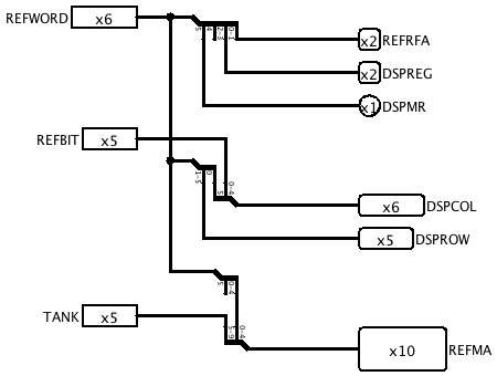 The purpose of this particular arrangement is to generate a display laid out as illustrated below.
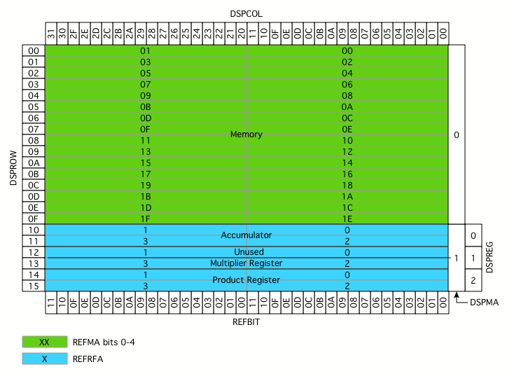 These subcircuits are connected on the main circut as follows.
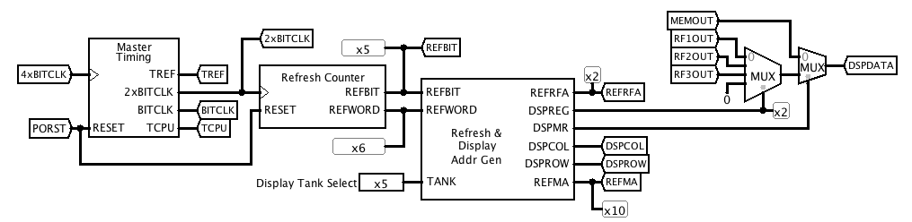 Multiplexers have been inserted into the memory and register file address lines to switch been refresh and CPU addresses, and some other minor changes made to ensure that things happen in the right phases of the BITCLK cycle.
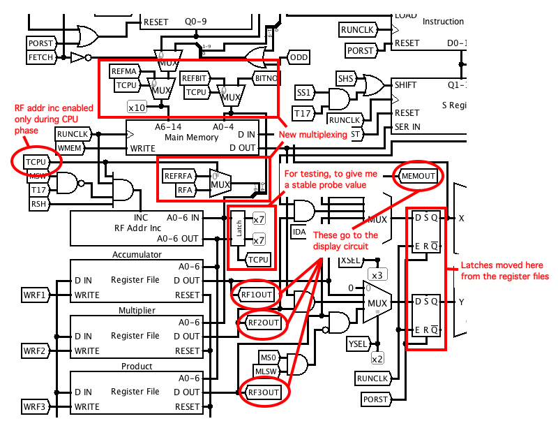 I moved the latches on the outputs of the register files out of the register file subcircuit and put them before the X and Y ALU inputs, because I need the raw outputs from the registers to send to the display. Also, I realised that I don't need to gate the write input to the static RAMs with RUNCLK, because this is already done when generating TWRITE. The register file simulation subcircuit is now just:
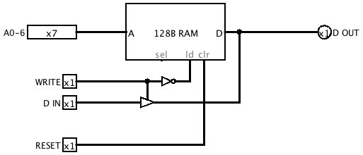
 I made the circuit symbol for the row driver one grid unit high, so that I could stack them up next to a decoder in the matrix driver (although this turned out not to help much, since I couldn't find a compact way to arrange the outputs).
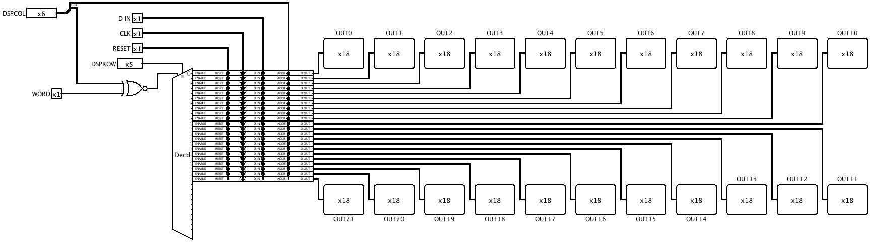 I designed the circuit symbol for the matrix driver to sit behind the LED matrix and provide a backdrop for it, as well as allowing two 18-wide matrices to be positioned side by side to form a 36 bit wide display.
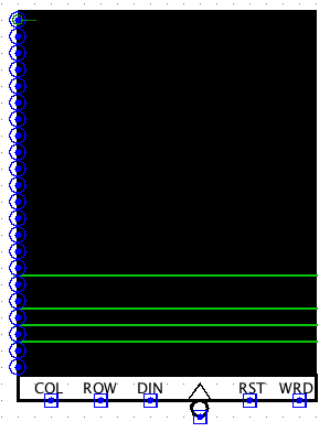 It took a bit of fiddling to get this to work properly, because the order in which Logisim draws overlapping components on a schematic seems to vary randomly depending on exactly how things are positioned, and to make things worse, it changes every time the circuit is reloaded from a file. But when the planets are aligned, it looks pretty good.