-
Starting on Phase Two
01/07/2021 at 03:31 • 0 commentsDown the Rabbit Hole and Back Again
Well, I got a bit distracted.
After the last log entry, I felt I was ready to embark on the second major phase of the project, in which I plan to build a second Logisim model based on real-world parts rather than generic Logisim ones.
I also want to be able to print out schematics from Logisim and use them to build from, which means showing pin numbers on schematic symbols, assigning designation numbers to components, etc. While these things can be done, Logisim doesn't give you much help with them. And there are complications – for example, a 7400 consists of four gates with different pin numbers, which means I would need to create four different library components for it, and be careful to use the right ones in the right places and not use the same gate twice or miss using a gate that I could have used. All very tedious and error-prone.
So, since Logisim is open source, I decided to take a couple of weeks to see if I could add a few things to it to make my life easier.
A few months later...
I now have a fork of Logisim-evolution that I'm calling Logisim-CAD. It allows a single library component to represent a part with multiple units. It has an auto-numbering feature that understands the multi-unit components. It also has a few tweaks to the rendering so that printed schematics come out looking nicer. For full details see the Readme on the Logisim-CAD Github page
Main Memory, Memory Timing and Refresh Timing
This is the first chunk of the Phase 2 model. It contains the DRAMs, timing DRAM cycles, and the timing chain that both refreshes the DRAM and generates data for the oscilloscope display.
I've divided the schematic into three parts here, although it's currently a single subcircuit in the Logisim model.
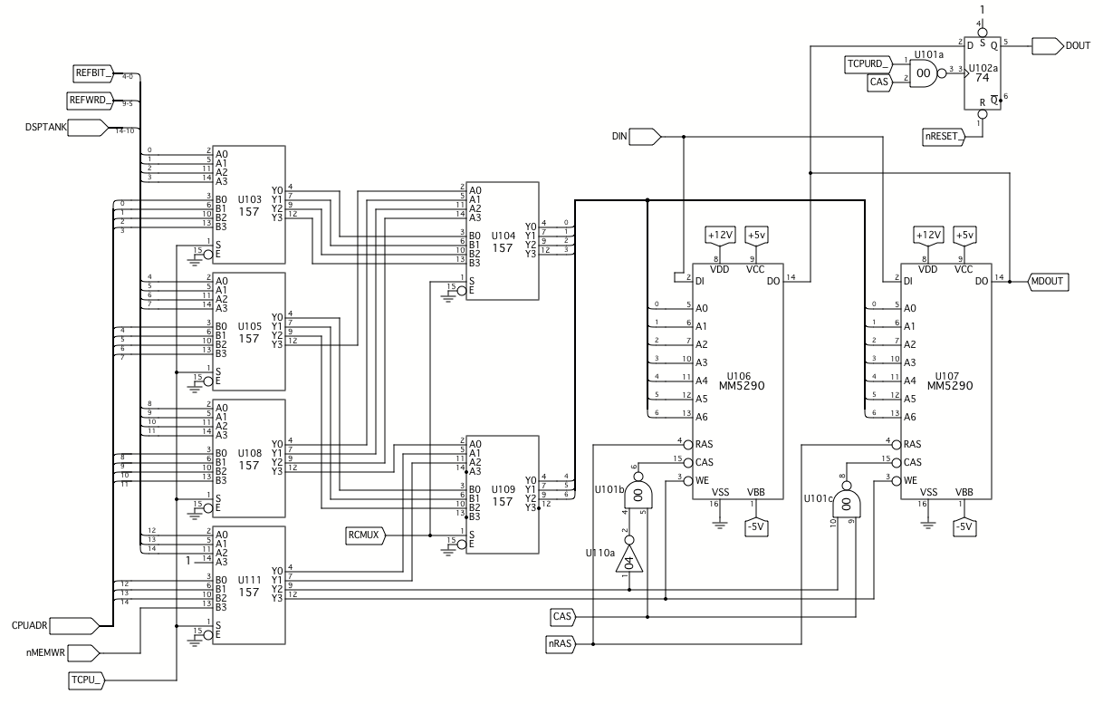
![]() There are two layers of multiplexers. U103, U105, U108 and U111 select either the CPU or display/refresh address. There are 15 address bits, leaving one input spare that is used to multiplex the write signal. U104 and U109 select the row and column addresses for the RAMs.
There are two layers of multiplexers. U103, U105, U108 and U111 select either the CPU or display/refresh address. There are 15 address bits, leaving one input spare that is used to multiplex the write signal. U104 and U109 select the row and column addresses for the RAMs.
U102a latches data read from the RAM during CPU memory cycles.![]() This is the timing chain for memory cycles. A 16MHz clock input is divided by U113a to give two 8MHz clocks of opposite phases. One of them drives U114a and b, which form a 4-state ring counter that generates the RAS (Row Address Strobe) and CAS (Column Address Strobe) for the RAMs. U113b is clocked from the other 8MHz phase and produces a signal that changes mid way between the falling edges of nRAS and nCAS; this is used to drive the row/column address multiplexers.
This is the timing chain for memory cycles. A 16MHz clock input is divided by U113a to give two 8MHz clocks of opposite phases. One of them drives U114a and b, which form a 4-state ring counter that generates the RAS (Row Address Strobe) and CAS (Column Address Strobe) for the RAMs. U113b is clocked from the other 8MHz phase and produces a signal that changes mid way between the falling edges of nRAS and nCAS; this is used to drive the row/column address multiplexers.
U115a is toggled for each memory cycle and partitions them into CPU cycles (TCPU) and display/refresh cycles (TREF). U115b further partitions the CPU cycles into read cycles (TCPURD) and potential write cycles (TCPUWR).
U102b synchronises the input from the reset switch so that the system-wide reset signal (nRESET) is released between active edges of the 8MHz clock, to ensure that everything starts off cleanly following a reset. I'm not sure if this is strictly necessary, but it seems like a good idea.![]() U115b also performs another function. U115b and U122 form a 5-bit counter configured to count from 0 to 17; this generates the display/refresh bit address (REFBIT). U116 and U123 form a 6-bit counter ranging from 0 to 43, from which the display/refresh word address (REFWRD) is derived. Each line of the display contains two words, so the upper 5 bits of REFWRD represent the display line number, ranging from 0 to 21. The first 16 lines show the page of memory selected by the TANK inputs, and the rest show data from the registers.
U115b also performs another function. U115b and U122 form a 5-bit counter configured to count from 0 to 17; this generates the display/refresh bit address (REFBIT). U116 and U123 form a 6-bit counter ranging from 0 to 43, from which the display/refresh word address (REFWRD) is derived. Each line of the display contains two words, so the upper 5 bits of REFWRD represent the display line number, ranging from 0 to 21. The first 16 lines show the page of memory selected by the TANK inputs, and the rest show data from the registers.
Also generated here are the display register file address (DSPRFA) and two synchronising signals for the display raster generator (DSPHSYNC and DSPVSYNC).
U120 combines the various sources of display data and produces a display video signal (DSPDAT). It consists of a short pulse at the end of each TREF cycle where a 1 is to be displayed. This will be connected to the Z input of the scope to produce bright dots on the screen. -
Automated Input Testing
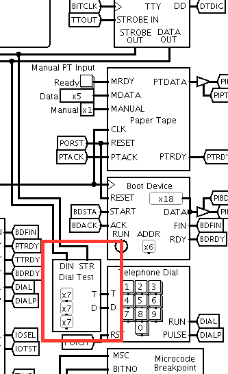
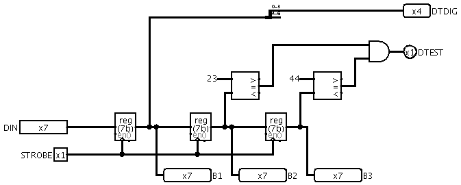
08/16/2020 at 11:21 • 0 commentsI added tests to the combined test suite for the Input instruction and the telephone dial input facility.
So that dial input could be tested automatically, I added a trigger circuit that watches the teletype output looking for the sequence of characters D#n, where n is a digit, and dials that digit.
Changes to main circuit
![]()
Dial test trigger subcircuit
![]()
Changes to dial simulator subcircuit
![]()
Additions to test program for input testing
# # INPUT instruction # Enter with AC = 0 # Exit with AC = 0 # Expected output: INP # I_test: O cI F I temp F A temp F L ^12 T temp F O temp F I temp F A temp F L ^12 T temp F O temp F O sp F # # Dial Input test # Enter with AC = 0 # Exit with AC = 0 # Expected output: D#5P # dial_test: O cD F O figs F O chash F O c5 F Z F O lets F A temp F S k_5 F F fail D O cP F O sp F -
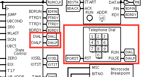
Telephone Dial
08/15/2020 at 13:54 • 0 commentsThe telephone dial is a somewhat unusual input device, as there is no way for the program to explicitly read it. When dial input is required, the program executes a Halt instruction. Dialling a digit n causes n to be added to the upper word of the accumulator (with the digit 0 giving n=10). Execution is then automatically resumed.
I expanded the IOSEL field to 3 bits so that I could add two more I/O sense inputs:
DIAL - high when the dial is turned away from its home position.
DIALP - goes high for each dial pulse.
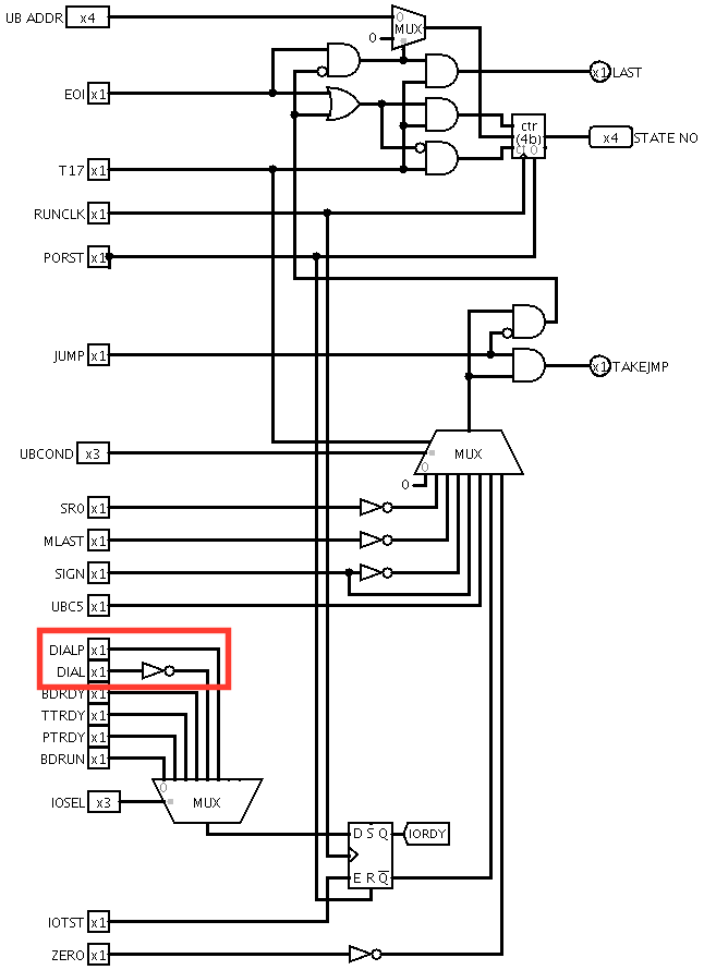
Inside the State Control subcircuit, DIAL is inverted so that the branch condition is true when dialling has finished.
DIAL is also connected to the Run Control circuit to trigger a NIMS to handle dial input.
Main circuit changes
![]()
State Control changes
![]()
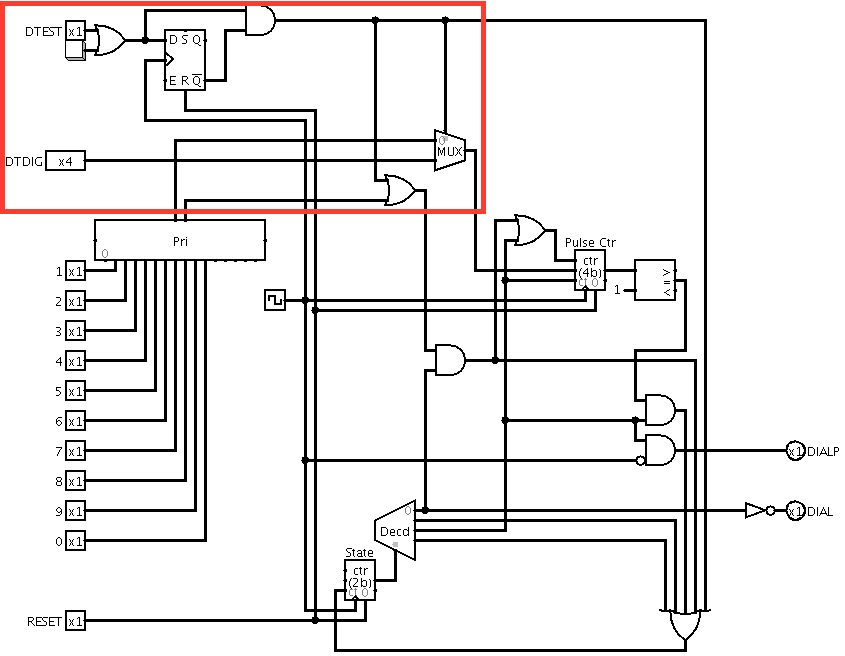
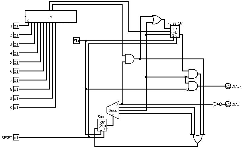
Dial Simulator
The dial simulator runs on a slow internal clock so that the computer simulation can keep up with it. It has 4 states. In State 0, it is paused waiting for a button to be pressed. When that happens, the digit dialled is loaded into the pulse counter and the state counter is allowed to advance. State 1 provides a delay. In state 2, pulses are generated at the DIALP output and the pulse counter counts down. When it reaches zero, the state counter advances again, through state 3 which provides another delay, and back to state 0.
![]()
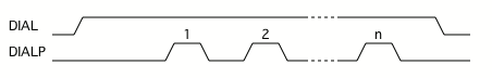
Dial Timing
![]()
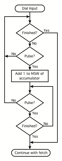
Dial Input Microcode
![]()
# IOSEL values for IOTST
TDFIN = 001  # Telephone dial finished
TDPUL = 101  # Telephone dial pulse

# Dial Input
   1 00011 0 0000 :  -   -   --  ---   -  --    -     -   --   -   -   -   -   -    -   IOTST   -   ---    TDFIN -  # If dialling finished
   1 00011 0 0001 :  -  EOI  --  ---   -  --    -     -   --   -   -   -   -   -    -   ----    -   BNIOT  0100     #   then continue program
   1 00011 0 0010 :  -   -   --  ---   -  --    -     -   --   -   -   -   -   -    -   IOTST   -   ---    TDPUL -  # If no dial pulse
   1 00011 0 0011 :  -   -   --  ---   -  --    -     -   --   -   -   -   -   -    -   ----    -   BNIOT  0000     #   then wait for pulse
   1 00011 0 0100 :  -   -   11  XAC   -  Y0   CY1    -   WAC  -   -  MSW LSW  -    -   ----    -   ---    ----     # Add 1 to MSW of accumulator
   1 00011 0 0101 :  -   -   --  ---   -  --    -     -   --   -   -   -   -   -    -   IOTST   -   ---    TDPUL -  # If no dial pulse
   1 00011 0 0110 :  -   -   --  ---   -  --    -     -   --   -   -   -   -   -    -   ----    -   BNIOT  0000     #   then wait for pulse
   1 00011 0 0111 :  -   -   --  ---   -  --    -     -   --   -   -   -   -   -    -   IOTST   -   ---    TDFIN -  # If dialling finished then continue
   1 00011 0 1000 :  -  EOI  --  ---   -  --    -     -   --   -   -   -   -   -    -   ----    -   BNIOT  1010     #   program else wait for no pulse
-
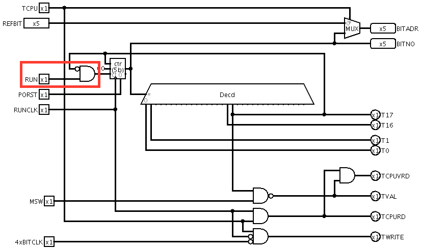
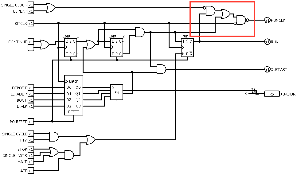
Bit Timing Change
08/13/2020 at 23:27 • 0 commentsI found another problem. When entering a NIMS, the first RUNCLK pulse, which is used to load the starting microcode address into the opcode register, was prematurely advancing the bit counter, skipping T0 of the first microinstruction.
To fix this, I modified the Bit Counter subcircuit so that the bit number is incremented only when RUN is true.
![]()
-
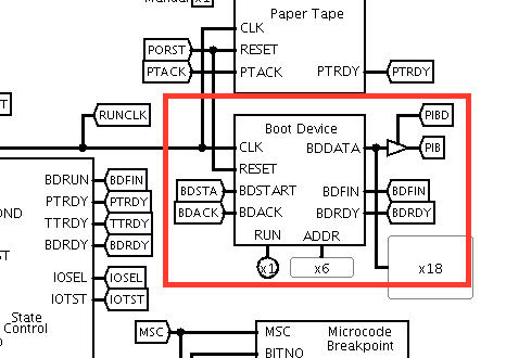
Bootstrapping
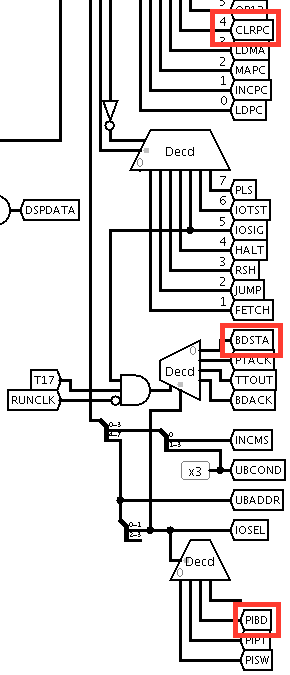
08/13/2020 at 09:41 • 0 commentsI created a boot device simulation and hooked it into the main circuit. To support booting, I added a PIBD value (boot device to PIB) for the IOSEL field, a CLRPC (clear program counter) operation and a BDSTA (boot device start) I/O signal.
I also changed the sense of the BDRUN input and renamed it to BDFIN (boot device finished), because it turned out I wanted to branch the other way on it in the microcode.Changes to main circuit
![]()
![]()
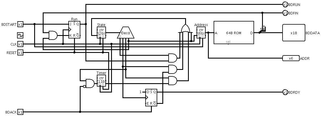
Boot Device Simulator
The boot device simulator is very similar to the paper tape simulator, with the addition of a flip flop to keep track of whether the boot device is running. The memory is 18 bits wide; 17 of them are used for boot data, and one is used to flag the last word of the data.
![]()
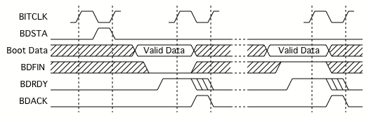
Boot Timing
![]()
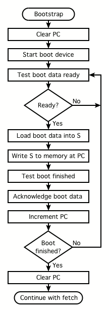
Boot Microcode
The boot sequence is entered when the Start button on the front panel is pressed. It first clears the PC, starts the boot device and then enters a loop reading words from the boot device and writing them to memory. Along with reading each word, BDFIN is tested; when it is true, the PC is cleared again and execution of the program begins.
![]()
# MISC values
CLRPC = 0011  # Clear PC

# PISEL values
PIBD = 01  # Boot device data to PIB

# IOSEL values for IOSIG
BDSTA = 00  # Start boot device
BDACK = 11  # Acknowledge boot device input

# IOSEL values for IOTST
BDFIN = 00  # Boot device is finished
BDRDY = 11  # Data available from boot device

# Boot
   1 00010 0 0000 :  -   -   --  ---   -  --    -     -   --   -   -   -   -   -    -   CLRPC   -   ---    ----     # Clear PC
   1 00010 0 0001 :  -   -   --  ---   -  --    -     -   --   -   -   -   -   -    -   IOSIG   -   ---    BDSTA -- # Start boot device
   1 00010 0 0010 :  -   -   --  ---   -  --    -     -   --   -   -   -   -   -    -   IOTST   -   ---    BDRDY -- # Test for boot data
   1 00010 0 0011 :  -   -   --  ---   -  --    -     -   --   -   -   -   -   -    -   ----    -   BNIOT  0100     # Loop until ready
   1 00010 0 0100 :  -   -   --  ---   -  --    -     -   --   -   -   -   -   -    -   PLS     -   ---    PIBD  -- # Load boot data into S
   1 00010 0 0101 : SHS  -   --  XSR   -  --    -    WMEM --   -   -   -   -   -    -   MAPC    -   ---    ----     # Write S to memory at PC
   1 00010 0 0110 :  -   -   --  ---   -  --    -     -   --   -   -   -   -   -    -   IOTST   -   ---    BDFIN -- # Test for boot finished
   1 00010 0 0111 :  -   -   --  ---   -  --    -     -   --   -   -   -   -   -    -   IOSIG   -   ---    BDACK -- # Ack boot data
   1 00010 0 1000 :  -   -   --  ---   -  --    -     -   --   -   -   -   -   -    -   INCPC   -   BNIOT  0100     # Inc PC and loop if boot not finished
   1 00010 0 1001 :  -  EOI  --  ---   -  --    -     -   --   -   -   -   -   -    -   CLRPC   -   ---    ----     # Clear PC and enter program
-
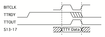
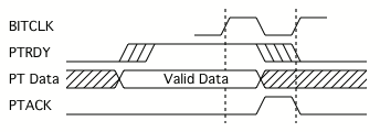
I/O Timing Diagrams
08/13/2020 at 09:37 • 0 commentsTeletype output timing
![]()
Paper tape input timing
![]()
-
Redesigning I/O
08/11/2020 at 06:40 • 0 commentsThe next thing I want to tackle is bootstrapping, or as the EDSAC team would have called it, "loading the initial orders".
I haven't decided exactly what form the bootstrap device will take yet, but I'm assuming it will be some kind of parallel input device that interfaces in a similar way to the paper tape reader. So before going any further I decided to make some changes to the way I/O devices are handled so I can treat them in a more uniform way.I/O condition testing
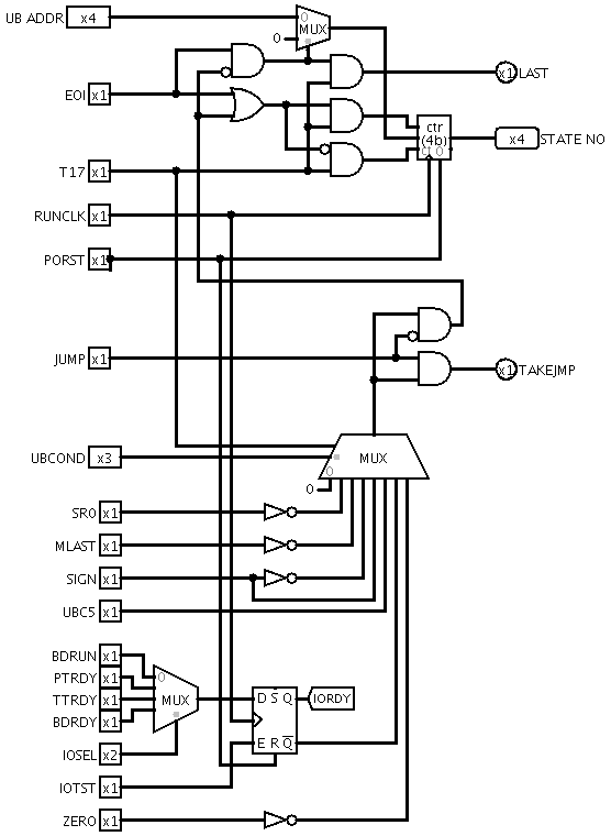
I didn't have any more branch condition inputs available, so I added an IOTST operation that samples one of four input conditions and latches it for branching on by a subsequent microinstruction. The conditions are assigned as follows:
PTRDY - data is available from the paper tape reader
TTRDY - teletype is ready to accept data
BDRDY - data is available from the boot device
BDRUN - boot device is running
TTRDY and PTRDY were previously connected directly to inputs of the branch condition multiplexer. One of those inputs is now called IORDY and is used to sense the condition latched by IOTST; the other is currently spare.
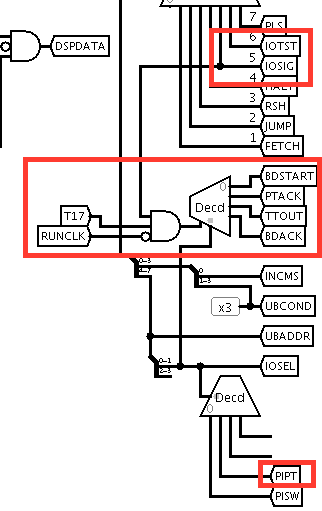
The condition to be tested by IOTST is selected by the IOSEL field, which again re-uses two bits from the UBRANCH field.I/O control signals
On the outwards side, there is an IOSIG operation that produces one of four output pulses during the second half of T17, selected by IOSEL.
PTACK - acknowledge data from paper tape reader
TTOUT - signal teletype that data is available
BDACK - acknowledge data from boot device
BDSTART - start the boot devicePaper tape input
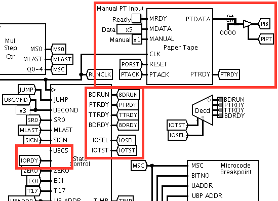
Input data from the paper tape is now read into the S register via the PIB, instead of having its own dedicated shift register.
Logisim Changes
Main circuit
![]()
![]()
State Control
![]()
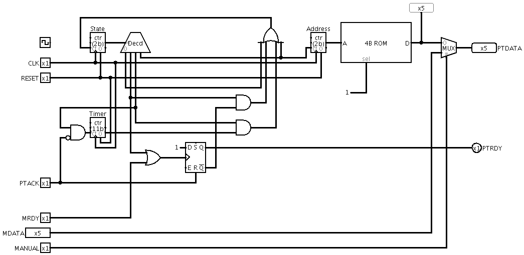
Paper tape simulation
For testing purposes, I put together a circuit that simulates a paper tape reader feeding in a few characters using the input device protocol. It incorporates a timer to slow down the input so that I can test whether the microcode correctly waits for the device to become ready.
![]()
New microcode for Input and Output instructions
# UBCOND values
BNIOT = 011  # I/O test false

# MISC values
IOSIG = 1010  # Generate I/O signal selected by IOSEL
IOTST = 0110  # Test I/O sense line selected by IOSEL

# PISEL values
PIPT = 10

# IOSEL values for IOSIG
PTACK = 10
TTOUT = 01
BDACK = 11

# IOSEL values for IOTST
BDRUN = 00
PTRDY = 10
TTRDY = 01
BDRDY = 11

# O - Output
   0 01001 0 0001 :  -   -   --  ---   -  --    -     -   --   -   -   -   -   -    -   IOTST   -   ---    TTRDY --  # Test TTY
   0 01001 0 0010 :  -   -   --  ---   -  --    -     -   --   -   -   -   -   -    -   ----    -   BNIOT  1000      # Loop until ready
   0 01001 0 0011 : SHS EOI  --  ---   -  --    -     -   --   -   -   -   -   -    -   IOSIG   -   ---    TTOUT --  # Read memory into S and signal TTY

# I - Input
   0 01000 0 0001 :  -   -   --  ---   -  --    -     -   --   -   -   -   -   -    -   IOTST   -   ---    PTRDY --  # Test paper tape
   0 01000 0 0010 :  -   -   --  ---   -  --    -     -   --   -   -   -   -   -    -   ----    -   BNIOT  1000      # Loop until ready
   0 01000 0 0011 :  -   -   --  ---   -  --    -     -   --   -   -   -   -   -    -   PLS     -   ---    PIPT  --  # Load paper tape data into S
   0 01000 0 0100 : SHS EOI  --  XSR   -  --    -    WMEM --   -   -   -   -   -    -   IOSIG   -   ---    PTACK --  # Write S to memory and ack paper tape
-
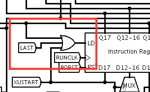
Fixing Instruction Register Timing
08/08/2020 at 01:53 • 0 commentsIt turns out that clocking the instruction register with BITCLK wasn't such a good idea, because its transitions occur slightly ahead of RUNCLK, and this was leading to glitchy behaviour.
So I came up with another solution to the problem that the change to the IR clocking was designed to solve. The IR is clocked with BITCLK as before, and the Run Control subcircuit lets through a RUNCLK pulse during a Continue pulse.
Changes to main circuit
![]()
Changes to Run Control
![]()
-
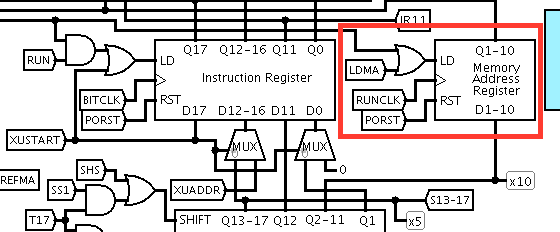
Front Panel Load Address Operation
07/28/2020 at 15:16 • 0 commentsThe way the data paths are set up, the easiest way to get a value from the switches to the PC is to go through the instruction register. However, I can't load the whole instruction register in the middle of a microcode sequence, because that would mess up the microcode address. So, I have split out the address part of the instruction register into a Memory Address register that I can load separately.
![]()
![]()
A quirk of this approach is that the value to be loaded into the PC needs to be set into switches 2 to 11, not 1 to 10 as might have been expected. This is due to the fact that IR/MA is loaded with an instruction during T17 of a fetch cycle, at which time the final shift of the value in the S register has not yet been performed; to compensate for this, inputs 0 to 16 of IR/MA are wired to outputs 1 to 17 of the S register.
This is not really a problem, it's just a matter of labelling the switches appropriately. I created a bezel for the switches on the main schematic showing where the hex digits go for PC values and data.
![]()
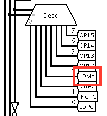
Load Address Microcode
# MISC values
LDMA  = 1101  # Load MA register from S register

# Load Address
   1 00001 0 0000 :  -   -   --  ---   -  --    -     -   --   -   -   -   -   -    -   PLS     -   ---    PISW -- # Load switches into S
   1 00001 0 0001 :  -   -   --  ---   -  --    -     -   --   -   -   -   -   -    -   LDMA    -   ---    ----    # Load MA from S
   1 00001 0 0010 :  -   -   --  ---   -  --    -     -   --   -   -   -   -   -    -   LDPC    -   ---    ----    # Load PC from MA
   1 00001 0 0011 :  -  EOI  --  ---   -  --    -     -   --   -   -   -   -   -    -   HALT    -   ---    ----    # Stop
-
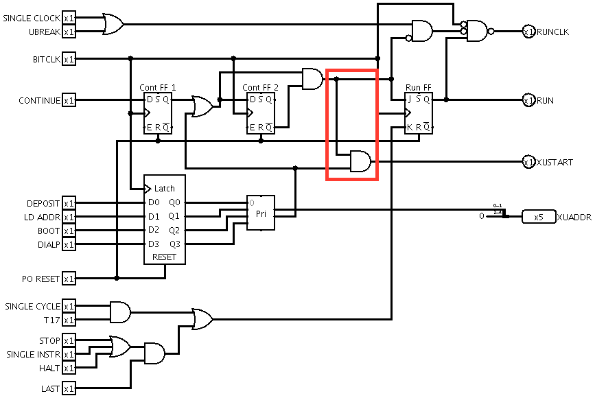
Corrections
07/28/2020 at 15:14 • 0 commentsI found a couple of problems. The first is that XUSTART was being asserted for as long as a button was held down, instead of just a single BITCLK cycle as intended. A small change to the Run Control subcircuit fixed this.
![]()
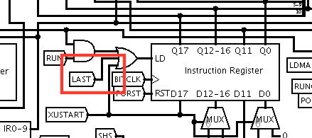
The second is that, on reaching the end of a NIMS, bit 17 of the instruction register was left as 1. This meant that subsequently pressing Continue without an intervening Reset would not start the program running, but instead just repeat the last executed NIMS.
To fix this, I arranged for the instruction register to be reloaded at the end of the NIMS. Since XUSTART is inactive by then, this sets IR17 to 0. The rest of the instruction register is loaded with whatever data happens to be in the S register at the time, but this does not matter, because every microinstruction sequence addressed by IR17=0 begins with a Fetch microinstruction.
![]()
 There are two layers of multiplexers. U103, U105, U108 and U111 select either the CPU or display/refresh address. There are 15 address bits, leaving one input spare that is used to multiplex the write signal. U104 and U109 select the row and column addresses for the RAMs.
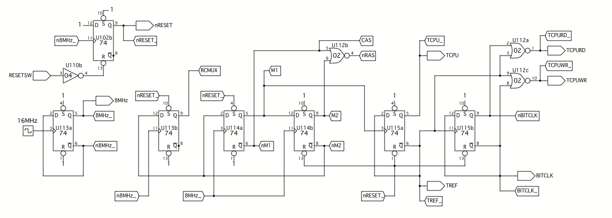 This is the timing chain for memory cycles. A 16MHz clock input is divided by U113a to give two 8MHz clocks of opposite phases. One of them drives U114a and b, which form a 4-state ring counter that generates the RAS (Row Address Strobe) and CAS (Column Address Strobe) for the RAMs. U113b is clocked from the other 8MHz phase and produces a signal that changes mid way between the falling edges of nRAS and nCAS; this is used to drive the row/column address multiplexers.
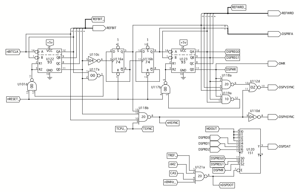 U115b also performs another function. U115b and U122 form a 5-bit counter configured to count from 0 to 17; this generates the display/refresh bit address (REFBIT). U116 and U123 form a 6-bit counter ranging from 0 to 43, from which the display/refresh word address (REFWRD) is derived. Each line of the display contains two words, so the upper 5 bits of REFWRD represent the display line number, ranging from 0 to 21. The first 16 lines show the page of memory selected by the TANK inputs, and the rest show data from the registers.