-
Left Shift Instruction
06/23/2018 at 11:20 • 0 commentsShifting the accumulator one bit to the left can be easily accomplished by adding it to itself. To shift by a variable number of bits, however, we will need to have a loop in the microcode, which brings us to the subject of microcode branching.
Microcode Branching
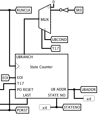
To support branching in the microcode, I added two new control fields: UBCOND (Microcode Branch Condition) and UBADDR (Microcode Branch Address).
UBCOND selects one of a number of branch conditions. The branching logic is as follows:- When the branch condition is true, the next value for STATENO is taken from the UBADDR field.
- When the branch condition is false and EOI is true, STATENO is reset to zero.
- Otherwise, STATENO is incremented.
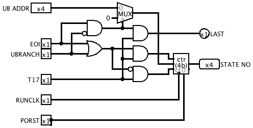
I made some additions to the State Counter subcircuit to implement this logic.
![]()
UBRANCH is a new input to the State Counter that is 1 when the selected branch condition is true. It is generated by a multiplexer in the main circuit:
![]()
Note that I changed how the LAST signal is generated again. It is now an output from the State Counter subcircuit, and is only activated if EOI is true and UBRANCH is false.
I have defined two UBCOND values so far:
UBCOND Branch condition 000 Always false 001 Bit 0 of the S Register = 0 Left Shift Instruction
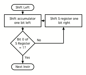
The number of places to shift is encoded in the Shift Left and Shift Right instructions by the position of the rightmost 1 bit in the instruction. This means we can take advantage of the fact that the instruction is left in the S Register at the end of the fetch cycle. Here's the strategy:
![]()
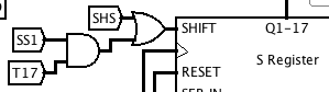
To do this, I added a control signal SS1 that shifts the S register only during T17. I used the bit that became spare when AND was removed.
![]()
Left Shift Microcode
The microcode for the Left Shift instruction takes 4 microinstructions, because it needs to shift all four short words of the accumulator. Shifting the S register is overlapped with both shifting the most significant accumulator short word, and with the branch back to the beginning if there is more shifting to be done. Note that the branch condition is testing the state of the S register before it is shifted.
# OPCODE L STAT : FETCH MASEL SHS EOI RFA WRF XSEL YSEL  CMX SS1 CY1 CYP ODD MSW LSW HALT WMEM UBCOND UBADDR

# L - Left shift
   11001 x 0001 :   0     0    0   0   00  10   10   10   0   0   0   0   0   0   1   0    0    000    0000
   11001 x 0010 :   0     0    0   0   10  10   10   10   0   0   0   0   0   0   0   0    0    000    0000
   11001 x 0011 :   0     0    0   0   01  10   10   10   0   0   0   0   0   0   0   0    0    000    0000
   11001 x 0100 :   0     0    0   1   11  10   10   10   0   1   0   0   0   1   0   0    0    100    1000
-
Register File Revision
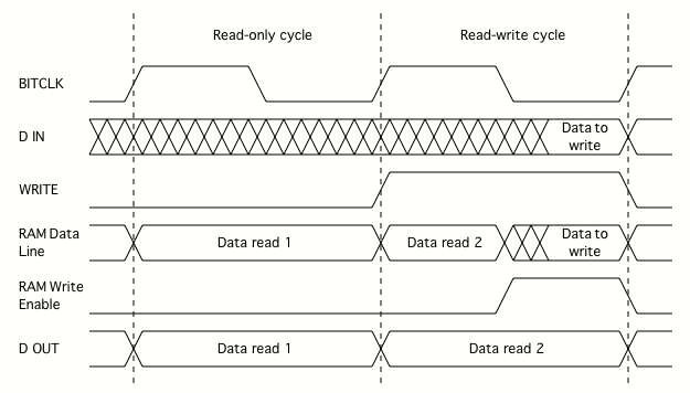
06/23/2018 at 06:19 • 0 commentsI replaced the output flip flop in the register file subcircuit with a transparent latch. This is mainly to aid debugging, so I can pause the simulation during phase 1 of a bit cycle and see the data read from the registers.
![]()
Revised timing diagram:![]()
-
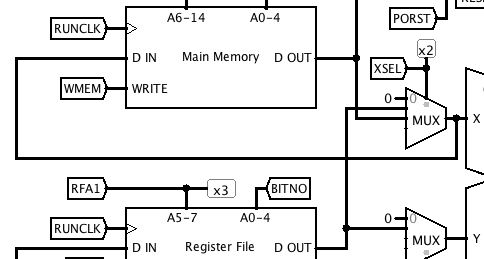
Load Multiplier and Collate Instructions
06/21/2018 at 11:17 • 0 commentsRearranging Registers and ALU Functions
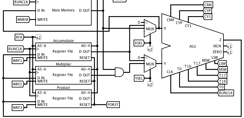
Until now I thought that I could keep the Multiplier and the Accumulator in the same register file because they wouldn't both need to be read at the same time. But it turns out that the Collate instruction is supposed to do this:
Accumulator <-- (Memory AND Multiplier) + Accumulatorso I need to add an additional register file to hold the Multiplier.
It also means the logical AND function isn't in the right place where I had it. I decided to move it out of the ALU and add an X input option that selects the AND of the Multiplier register and data read from memory. The ALU can then be configured to add this to the Accumulator, accomplishing the Collate operation in one short or long word cycle.
This is the relevant part of the revised data path. There are now separate register files for the Accumulator and Multiplier, and I also added one for the Product register while I was at it. The RFA1 microinstruction field has been reduced to 2 bits and renamed simply RFA, since it supplies the high-order address bits for all the register files. The AND control signal has been removed.
![]()
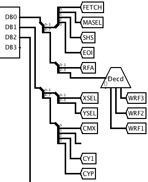
The WRF1 field has been replaced with a 2-bit field that is decoded to produce write signals for the three register files:
![]()
Revised ALU with logical AND function removed:![]()
Microcode
We can now microcode the H instruction, which loads a word from memory into the Multiplier register, and the C (Collate) instruction.
# OPCODE L STAT : FETCH MASEL SHS EOI RFA WRF XSEL YSEL CMX     CY1 CYP ODD MSW LSW HALT WMEM

# H - Load Multiplier
   10101 0 0001 :   0     1    0   1   11  01   01   00   0   0   0   0   0   1   1   0    0

   10101 1 0001 :   0     1    0   0   01  01   01   00   0   0   0   0   0   0   1   0    0
   10101 1 0010 :   0     1    0   1   11  01   01   00   0   0   0   0   0   1   0   0    0

# C - Collate
   11110 0 0001 :   0     1    0   1   11  10   10   01   0   0   0   0   0   1   1   0    0

   11110 1 0001 :   0     1    0   0   01  10   10   01   0   0   0   0   0   0   1   0    0
   11110 1 0010 :   0     1    0   1   11  10   10   01   0   0   0   0   1   1   0   0    0
-
Transfer Instructions
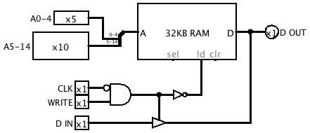
06/20/2018 at 10:56 • 0 commentsThe two Transfer instructions, T and U, transfer the contents of the accumulator to the main memory. The difference between them is that T also clears the accumulator, whereas U does not.
These are the first instructions we've implemented so far that write to main memory, so we need a new control signal, WMEM. This is gated with phase 2 of the bit clock so that writing to memory occurs only during the write phase of each bit time.
Updated main memory subcircuit:
![]()
I also made a change to the data path in the main circuit. Instead of the data input to the main memory coming from the output of the ALU, it now comes from the multiplexer feeding the X input of the ALU. This will enable me to clear the accumulator at the same time as writing it to main memory for implementing the T instruction.
Revision to the main circuit:
![]()
Microcode
The T instruction selects the accumulator as the source for both inputs to the ALU, and enables writing to memory. It also sets the ALU to perform subtraction, thereby subtracting the accumulator from itself, giving zero, and writes this back to the accumulator.
The U instruction simply selects the accumulator as the X input and writes it to memory.
# OPCODE L STAT : FETCH MASEL SHS EOI RFA1 WRF1 XSEL YSEL CMX AND CY1 CYP ODD MSW LSW HALT WMEM

# T - Transfer and clear
   00101 0 0001 :   0     1    0   1   110   1   10   10   1   0   1   0   0   1   1   0    1

   00101 1 0001 :   0     1    0   0   010   1   10   10   1   0   1   0   0   0   1   0    1
   00101 1 0010 :   0     1    0   1   110   1   10   10   1   0   0   1   1   1   0   0    1

# U - Transfer without clear
   00111 0 0001 :   0     1    0   1   110   0   10   00   0   0   0   0   0   0   0   0    1

   00111 1 0001 :   0     1    0   0   010   0   10   00   0   0   0   0   0   0   0   0    1
   00111 1 0010 :   0     1    0   1   110   0   10   00   0   0   0   0   1   0   0   0    1
-
Subtract and Halt Instructions
06/19/2018 at 12:55 • 0 commentsSubtract
Microcode for the Subtract and Subtract Long instructions is very similar to the Add instructions, the only differences being the activation of CMX and CY1.
# OPCODE L STAT : FETCH MASEL SHS EOI RFA1 WRF1 XSEL YSEL CMX AND CY1 CYP ODD MSW LSW

# S - Subtract
   01100 0 0001 :   0     1    0   1   110   1   01   10   1   0   1   0   0   1   1

   01100 1 0001 :   0     1    0   0   010   1   01   10   1   0   1   0   0   0   1
   01100 1 0010 :   0     1    0   1   110   1   01   10   1   0   0   1   1   1   0
Halt
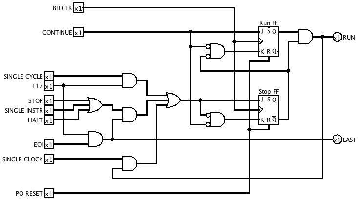
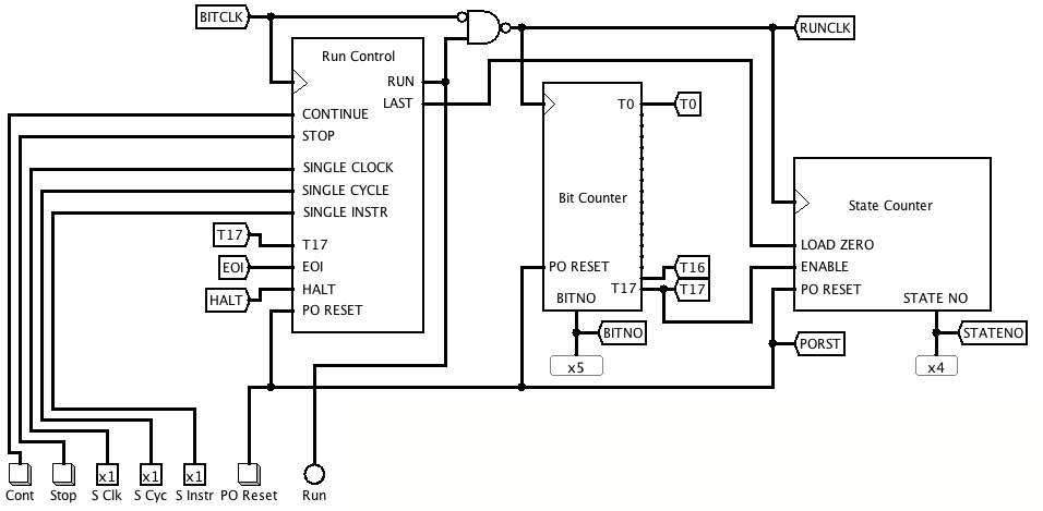
To facilitate running test programs of more than one or two instructions, it seemed like it would be helpful to implement the Halt instruction next. I added a HALT control signal that becomes a new input to the Run Control subcircuit. I also tidied up the Run Control logic a bit, renaming some of its inputs for consistency, and moving generation of the LAST signal from the main circuit into the Run Control subcircuit.
This is the new Run Control circuit:
![]()
This is how it fits into the main circuit:
![]()
Microcode for the Halt instruction is now straightforward.
# OPCODE L STAT : FETCH MASEL SHS EOI RFA1 WRF1 XSEL YSEL CMX AND CY1 CYP ODD MSW LSW HALT

# Z - Halt
   01101 0 0001 :   0     0    0   1   000   0   00   00   0   0   0   0   0   0   0   1
-
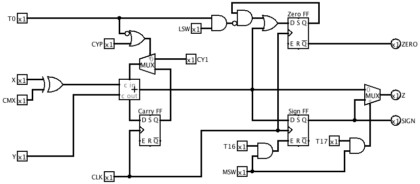
Sign and Zero Flags
06/18/2018 at 12:57 • 0 commentsA small revision
While thinking about the features below, I realised that I needed separate signals indicating the most significant word of an operation and forcing the memory address to be odd, so I renamed the signal I was previously calling MSW to ODD, and added a new MSW signal.
Sign and Zero Flags
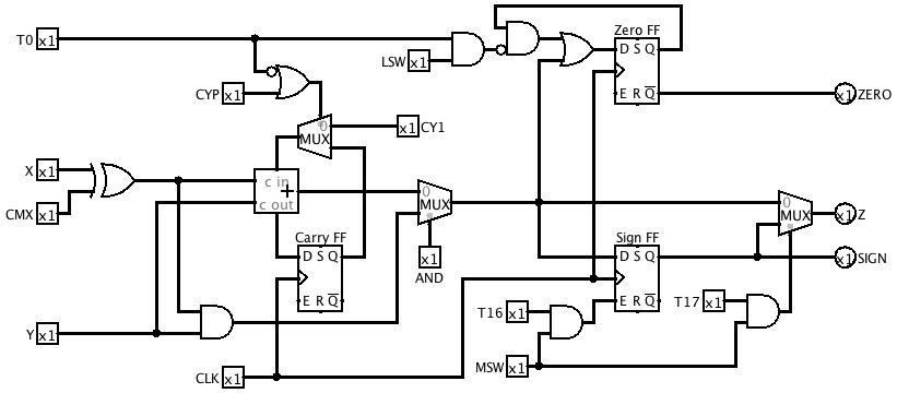
There are two more things we will want the ALU to do for us, and that is to provide outputs indicating the sign of a result, and whether the result was negative. The revised ALU subcircuit below implements these.
![]()
The Sign FF captures the sign bit, which is bit 16 of the most significant short word of the result. The sign bit is also replicated into the most significant bit of the result, thereby sign-extending it from 17 to 18 bits (or from 35 to 36 bits for a long word). The extra bit is usually ignored, but will play a role in multiplication later.
The Zero FF keeps track of whether thre are any non-zero bits in the result. It is set equal to the result during T0 of the least significant word, and then set to 1 if any 1 bit occurs thereafter. At the end of the operation, its complement becomes the ZERO output of the ALU.
There are two new control inputs to the ALU. LSW is activated during the least significant word of an operation, and MSW during the most significant word. For a short word operation, both are activated.
Microcode
Here is the revised microcode for the Add instructions.
# OPCODE L STAT : FETCH MASEL SHS EOI RFA1 WRF1 XSEL YSEL CMX AND CY1 CYP ODD MSW LSW

# A - Add
   11100 0 0001 :   0     1    0   1   110   1   01   10   0   0   0   0   0   1   1

   11100 1 0001 :   0     1    0   0   010   1   01   10   0   0   0   0   0   0   1
   11100 1 0010 :   0     1    0   1   110   1   01   10   0   0   0   1   1   1   0
-
Add Long Instruction
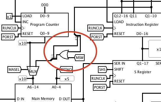
06/17/2018 at 13:57 • 0 commentsA small addition to the memory addressing logic is needed to support long word instructions. A new control signal MSW indicates that the most significant short word of a long word is being addressed, and forces the LSB of the address to 1.
![]()
We can now microcode the long-word variant of the Add instruction as follows.
# OPCODE L STAT : FETCH MASEL SHS EOI RFA1 WRF1 XSEL YSEL CMX AND CY1 CYP MSW

# Add Long
   11100 1 0001 :   0     1    0   0   010   1   01   10   0   0   0   0  0
   11100 1 0010 :   0     1    0   1   110   1   01   10   0   0   0   1  1
-
Microcoding and Testing the Add Instruction
06/17/2018 at 02:43 • 0 commentsMicrocode for the Add instruction
Here's the microcode for the short-word version of the Add instruction.
# OPCODE L STAT : FETCH MASEL SHS EOI RFA1 WRF1 XSEL YSEL CMX AND CY1 CYP
# A - Add
   11100 0 0001 :   0     1    0   1   110   1   01   10   0   0   0   0
MASEL = 1 selects the address field of the instruction as the main memory address. RFA1 = 011 (remember the data bits are backwards in the microcode source) selects the most significant short word of the accumulator. XSEL = 10 and YSEL = 01 route data read from main memory and register file 1 to the ALU, which is set up for addition with carry in = 0. WRF1 = 1 writes the output from the ALU into register file 1. EOI = 1 indicates that this is the last microinstruction for this instruction.
Test Loader
I wrote a Python program to generate memory images for loading into Logisim. It accepts a subset of the EDSAC Initial Orders 2 input format, with a few extensions.
Here's an example for testing the Add instruction.
0: A 2 F
1: A 3 F
2: 123
3: 456
The numbers on the left are memory addresses, in decimal. Lines starting with a letter represent instructions, and consist of an opcode, a memory address, and a length indicator (F for short word, D for long word). A line can also contain a number to be stored in memory, written in decimal, hex (prefixed by $) or binary (prefixed by %).
Assuming the accumulator starts out containing zero, if the test is successful it should end with the accumulator containing 579 decimal (10 0100 0011).
Add Test Video
Here's a video of the Add test running in Logisim. Note that the numbers appear LSB first in Logisim's memory display windows.
-
Registers and ALU
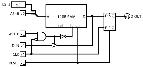
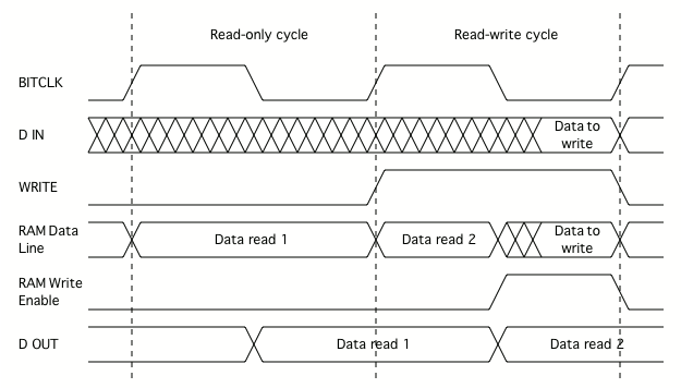
06/17/2018 at 02:36 • 0 commentsRegister File
There will eventually be two of these, one holding the Accumulator and Multiplier Registers (which won't need to be accessed at the same time) and one holding the Product Register.
![]()
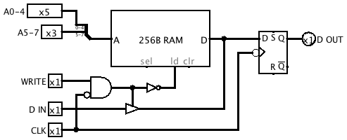
This subcircuit incorporates logic to support the division of each bit period into a Read and a Write phase. Data is read from the RAM when the clock is high and latched into the output flip-flop on the falling edge of the clock. Writing to the RAM is enabled when the WRITE control input is active and the clock is low.
![]()
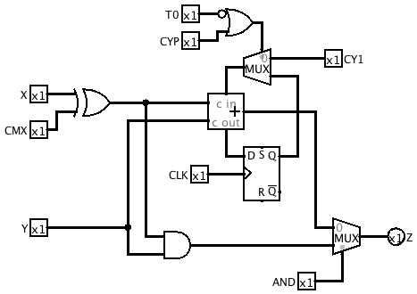
ALU
The ALU is built around a one-bit full adder with a flip-flop to hold the carry between bits. Additional logic allows one of the inputs to be complemented (CMX = 1), and a logical AND operation to be selected instead of the adder output (AND = 1).
![]()
The CYP and CY1 inputs control the carry input to the adder during T0. When CYP = 0, the carry in is equal to CY1, otherwise the carry out from the previous cycle is used. During all other bit times, the carry out from the previous bit is used.
Useful combinations of control inputs include:
CYP CY1 CMX AND Result 0 0 0 0 Y + X 0 1 0 0 Y + X + 1 1 x 0 0 Y + X with carry in 0 1 1 0 Y - X 0 0 1 0 Y - X - 1 1 x 1 0 Y - X with carry in x x x 1 Y AND X Updated Main Circuit
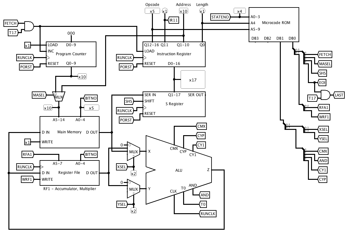
Here's the main circuit with the ALU and one of the register files added.
![]()
The following microinstruction fields have also been added:
EOI End of Instruction Indicates the last short word cycle of an instruction. Causes LAST to be activated during T17. RFA1 Register File 1 Address Selects one of 8 short words in Register File 1. WRF1 Write Register File 1 Causes the output of the ALU to be written into Register File 1. XSEL X Select Selects the source for ALU input X. YSEL Y Select Selects the source for ALU input Y. CMX Complement X ALU control inputs AND Logical AND CY1 Carry in value CYP Use previous carry XSEL values:
00 Constant 0 01 Register File 1 10 Main Memory 11 Currently unused YSEL values:
00 Constant 0 01 Register File 1 10 Currently unused 11 -
Microassembler and Fetch Test
06/14/2018 at 11:46 • 0 commentsI wrote a simple assembler in Python for the microcode.
Here's what the microcode for fetching an instruction looks like:
AddressBits = 10
DataBits = 15

# OPCODE D STAT : FETCH MASEL SHS

# Fetch
   xxxxx x 0000 :   1     0    1
Lines beginning with # are comments. After a header indicating how many address and data bits to expect, there are lines containing an address and some data bits separated by a colon. The data bits are in reverse order, with bit 0 on the left; I did that so I could add more microinstruction bits easily without having to reformat things. Any unspecified high-order data bits are padded with 0.
The 'x' characters in the address are don't-care bits. The reason for them is that I'm planning to use a trick that Ben Eater used in his breadboard computer, and repeat the instruction-fetching microcode at the beginning of the microcode for every instruction. When the microassembler sees don't-care bits in an address, it fills in all matching address combinations with the same data.
The output of the microassembler is a file suitable for loading into a Logisim memory component.
Instruction Fetch Test Video
Here's a video showing the above microcode being tested in Logisim.