Close
0%
0%

ULX3S powerful ECP5 board for open source FPGA

University digital Logic Learning Xtensible board release 3 with SDRAM

Similar projects worth following
A powerful ECP5 board for open source FPGA development


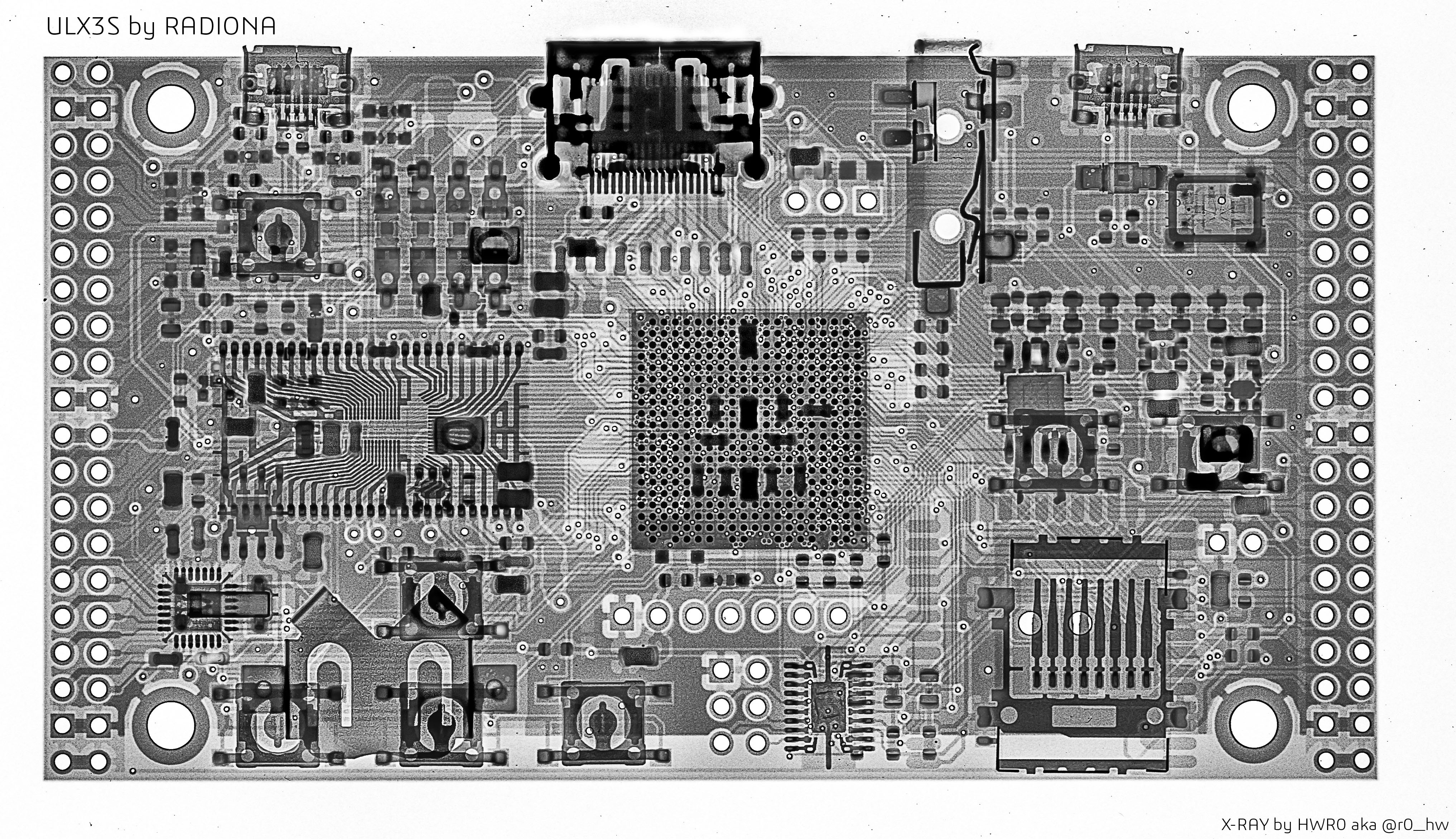
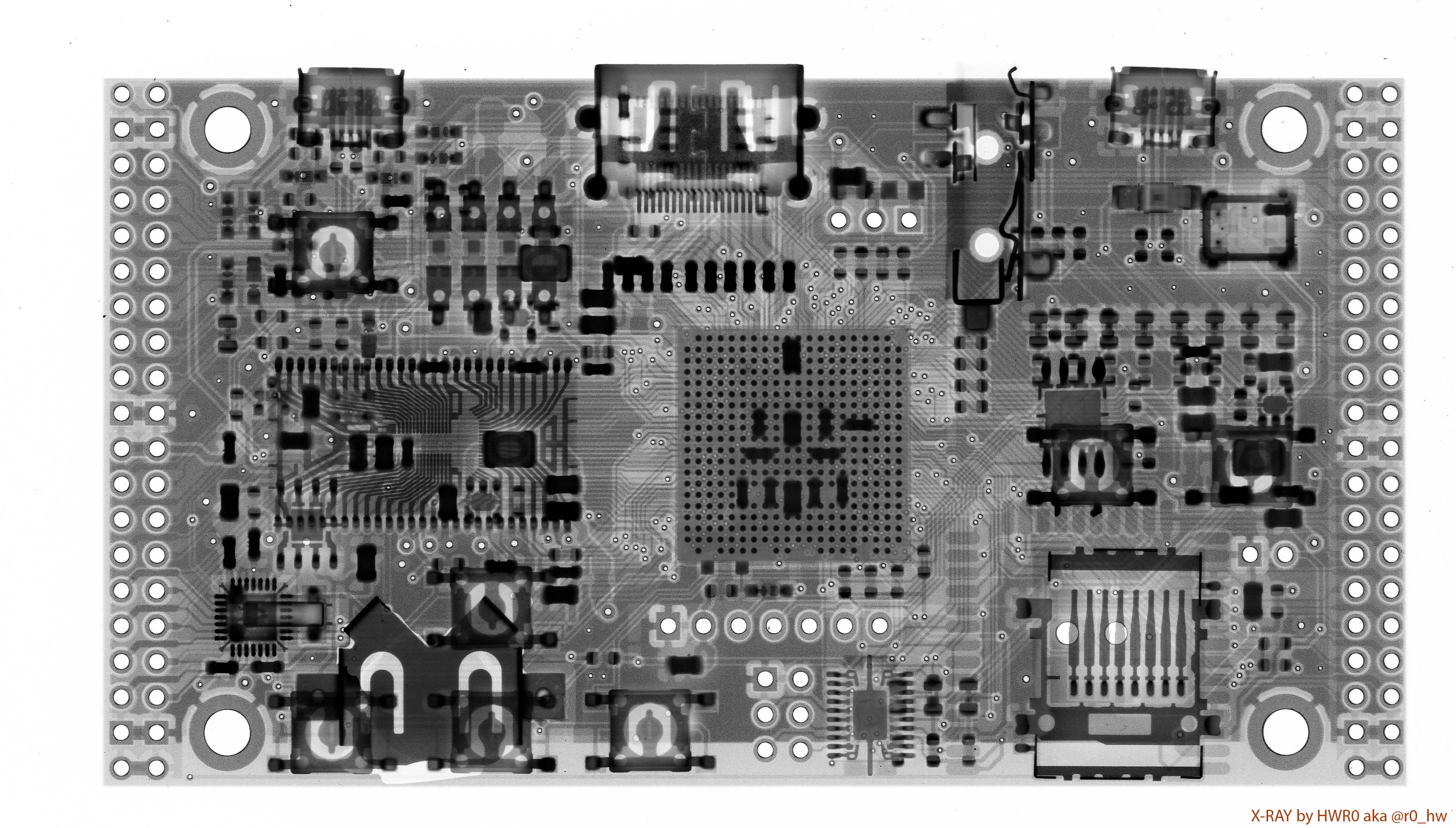
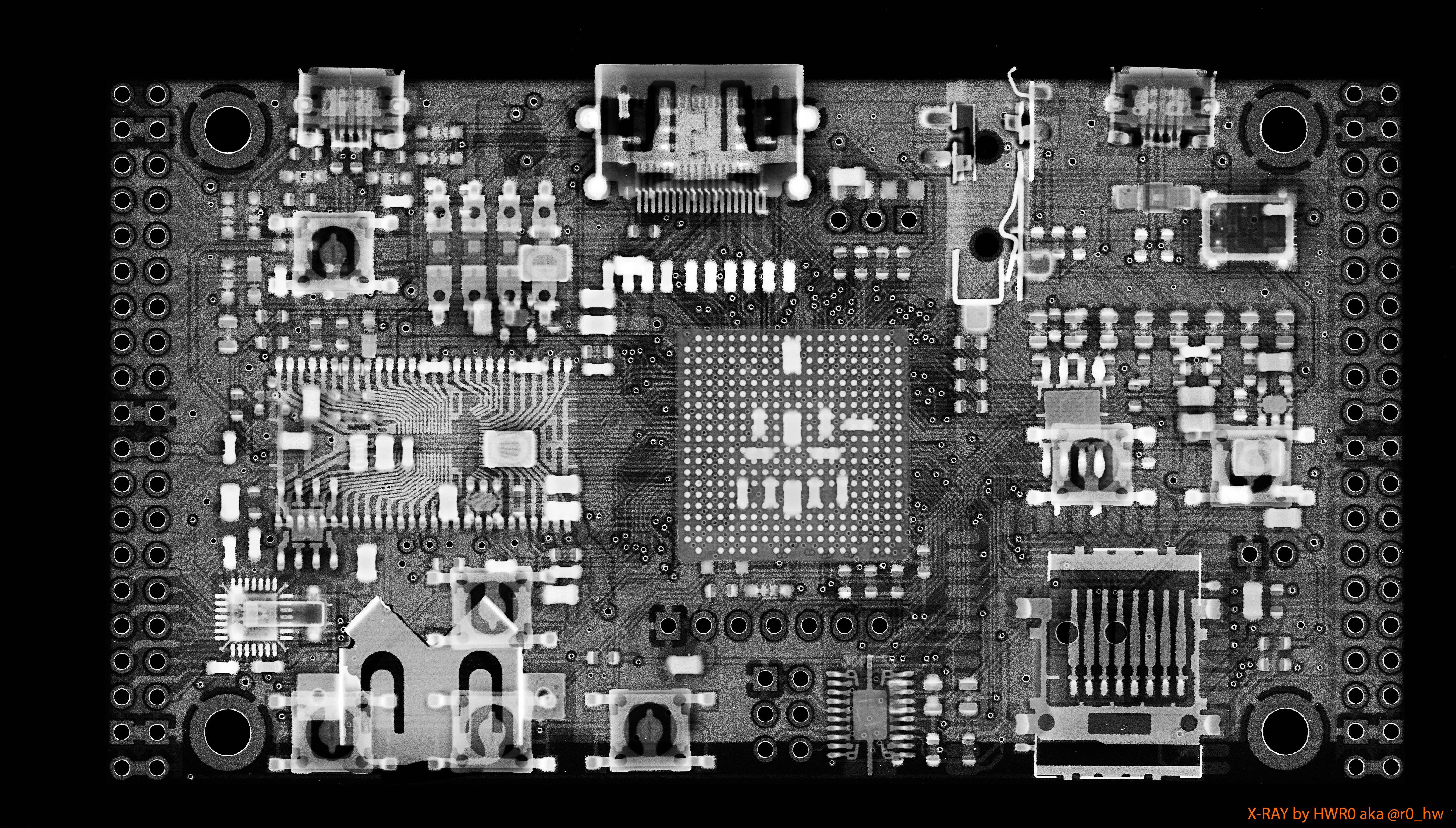
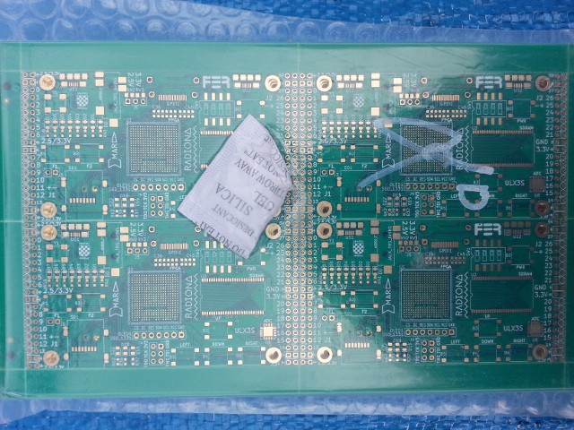
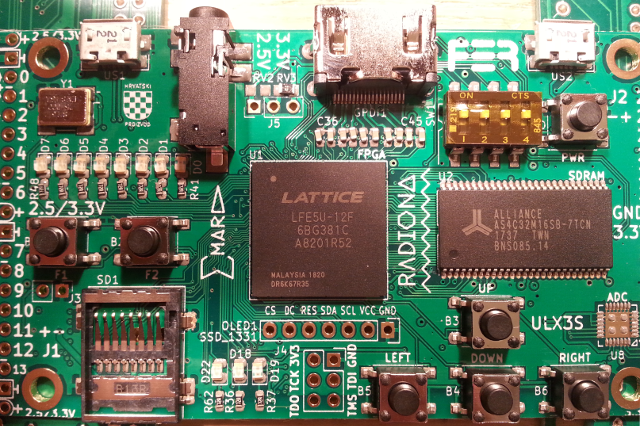
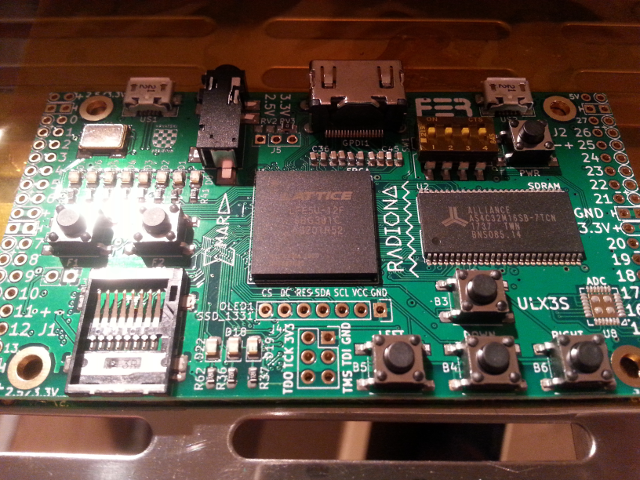
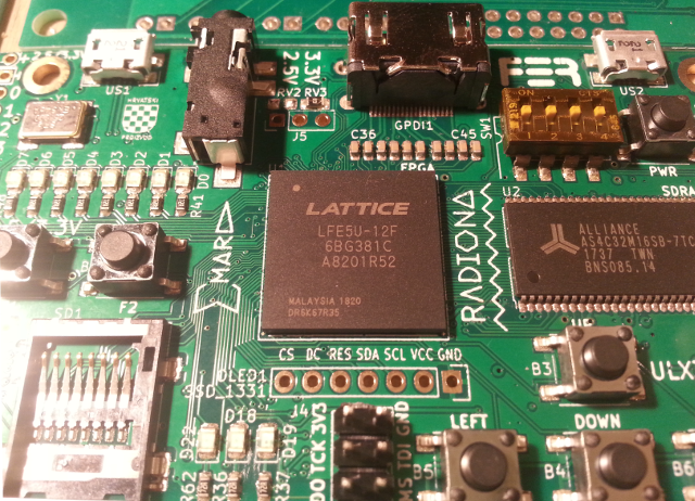
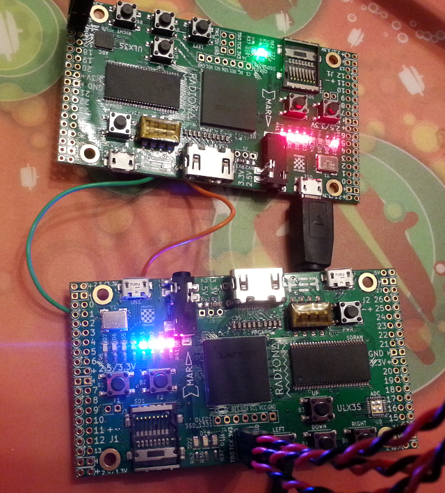
The ULX3S is a fully open source, compact, robust and affordable FPGA board equipped with a balanced spectrum of extra components and expansions. Although primarily developed as a teaching tool for mastering the principles of digital circuit design 1, a wide selection of useful features and interfaces enables it to serve as a broad spectrum module for installation in complex devices.

ULX3S webpage

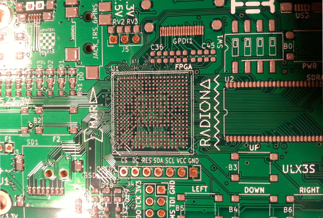
ULX3S uses powerful Lattice Semiconductor ECP5 series FPGA chip supported by the latest open-source toolchains. This makes the ULX3S one of the most powerful and desirable platforms for FPGA enthusiasts available today. ULX3S comes equipped with onboard WiFi, display, buttons, LEDs and storage. Flash it using the WiFi connection (over-the-air update), or with one of the bitstreams stored on SD card and browsed by onboard OLED display and buttons. Due to its battery-backed RTC, it can power down completely and wake up only on certain events making it useful for low power applications such as battery-powered remote sensor nodes. And if you’re not of the low-power type, onboard peripherals such as SDRAM, USB, Digital video out, onboard FM/ASK antenna, ADC and DAC can make it audio/video powerhouse for signal processing and synthesis, motor control or SDR cases. You can emulate arcade machines or retro computers like Minimig(Amiga) or modern systems like F32C (MIPS/RISCV). It has 56 GPIO pins, all routed as differential pairs and a PMOD compatible pinout, opening it to a wide range of expansion options. If you are just starting with FPGA, you can also use the ULX3S as powerful Arduino and program it using Arduino IDE in seconds.

It has been actively developed since 2016 and is the result of collaboration between Radiona.org / Zagreb Makerspace and FER – Faculty of Electrical Engineering and Computing – University of Zagreb, Croatia.
1 ULX3S is beeing actively used in Digital Logic class at the University of Zagreb Faculty of Electrical Engineering and Computing, Croatia

Features

FPGA: Lattice ECP5 LFE5U-85F-6BG381C (85K LUT)

USB: FTDI FT231XS (300kbit JTAG and 3Mbit USB-serial)

GPIO: 56 pins (28 differential pairs), PMOD-friendly

RAM: 32MB SDRAM MT48LC16M16

Flash: 4MB Quad-SPI Flash IS25LP032D for FPGA config

Storage: Micro-SD slot

LEDs: 11 (8 blink-LEDs, 2 USB LEDs, 1 WiFi LED)

Buttons: 7 (4 direction, 2 fire, 1 power button)

Audio: 3.5 mm jack with 4 contacts (analog stereo + digital audio or composite video)

Video: GPDI connector with 3.3V-5V I2C bidirectional level shifter

Display: placeholder for 0.96" SPI COLOR OLED

WiFi+bluetooth: placeholder for ESP-32 (Standalone JTAG web interface over WiFi)

ADC: 8 channels, 12 bit, 1 MSa/s MAX11125

Power: 3 Switching voltage regulators: 1.1V, 2.5V, 3.3V

Clock: 25 MHz onboard, external differential clock input

Low power sleep: RTC clock wakeup, power button, 32768 Hz quartz and battery

GPDI is General Purpose Differential Interface, Electrically LVDS, mostly TMDS tolerant female receptacle more-or-less compatible with digital monitors/TVs

View all 27 project logs

View all instructions

Enjoy this project?

Share

Discussions

AlanH wrote 05/30/2020 at 06:18 point

Curious where you get your PCBs made that can handle the tight annular rings you have around your vias (~4.3mils or .1095 mm)?  Also how do you mount the BGAs?

  Are you sure? yes | no

kwapiszon wrote 02/18/2020 at 11:53 point

fajne, ale dobrze było by dodac coś co by było bardziej pełne.

zasilanie, ekran, klawiatura, coś jak tutejsze ello2 (sprawdz proszę), cos co ma na dzień dobry coś co działa (risc-v ma wiele implementacji na fpga) może jakas konsola.

Coś co klient kupuje, wrzuca baterie i ma gotowy produkt. Wtedy nierozgarnięci programiści (a wszyscy tacy są) mogę poprawić oprogramowanie.

FPGA może działać niesamowicie wydajnie. Emulator macintosha 8Mhz OS 7 powinien na tym pójść i jeszcze pracować na dwóch paluszkach przez godziny (albo na lekko wiekszych 18650), gdyby można to było zabrac ze sobą i pisac po prostu teksty, terminal ssh, edytor dla pisarzy to miało by sens a ludzie wycisnęli by siódme poty z procesora i baterii.

Zatem więcej power (np. dodanie lipo zasilania), sterownika do klawiatury i ekranu i gotowy soft do robienia JEDNEJ rzeczy. Inaczej to bedzie nisza niszy
 a tego nie chcemy. Ja nie chcę, ja chce uzywac takiego sprzętu.

  Are you sure? yes | no

Andrey V wrote 07/20/2019 at 05:40 point

Iteresting progect. But for the educational needs it is better to have a standart arduino or(and) raspberry pi connector(with level shifters onboard)

  Are you sure? yes | no

Hexastorm wrote 05/02/2019 at 08:34 point

impressive board... A bit of topic; As you might see from my Hackaday page,  I am building a laser scanner.. One of the things I want to improve is the data speed.  Could you or do you know of a very basic example which can be used to write data to the SDRAM or SDcard via the FPGA and also to read data from the SDRAM/SDCARD and write it to say a LED. Should I use a SDRAM or a SDCARD?  If I read out the data, one bit wide, at a rate of 20 MHz, can I do this process continuously via a ringbuffer or do I need to do it batch wise. To clarify; continously expose with the laser and retrieve data or first write the data to the memory and then read the data from the memory.  Preferably... examples are as easy as possible.

  Are you sure? yes | no

radiona.org wrote 05/03/2019 at 06:05 point

Hi, this is answer from EMARD

This laser scanner is great project!

I think both SDRAM and SDCARD methods are possible

although I personally haven't tried them so I can't point

now to exact example but it shouldn't be difficult to make either.

For SDRAM method you can take any driver from the net,

chances are that its source already contains a testbench code

that does exactly this, bulk write and read for verification

However there could be some random latency of SDRAM

therefore few KB of fast FIFO or cache should be applied

(available as block RAM at all FPGA chips)

Similar could be with SDCARD also it's a SPI interface and

after some initialization it should also be possible to write data.

I don't know about latency, it's probably significant so I guess

SDRAM should be used as buffer


  Are you sure? yes | no

kylix34 wrote 04/27/2019 at 05:34 point

Nice job, Goran!!!!

  Are you sure? yes | no

Goran Mahovlic wrote 04/26/2019 at 16:09 point

Tnx!

  Are you sure? yes | no

linkret wrote 04/26/2019 at 13:04 point

Pretty cool, not that expensive, many features

  Are you sure? yes | no

Similar Projects

Does this project spark your interest?

Become a member to follow this project and never miss any updates