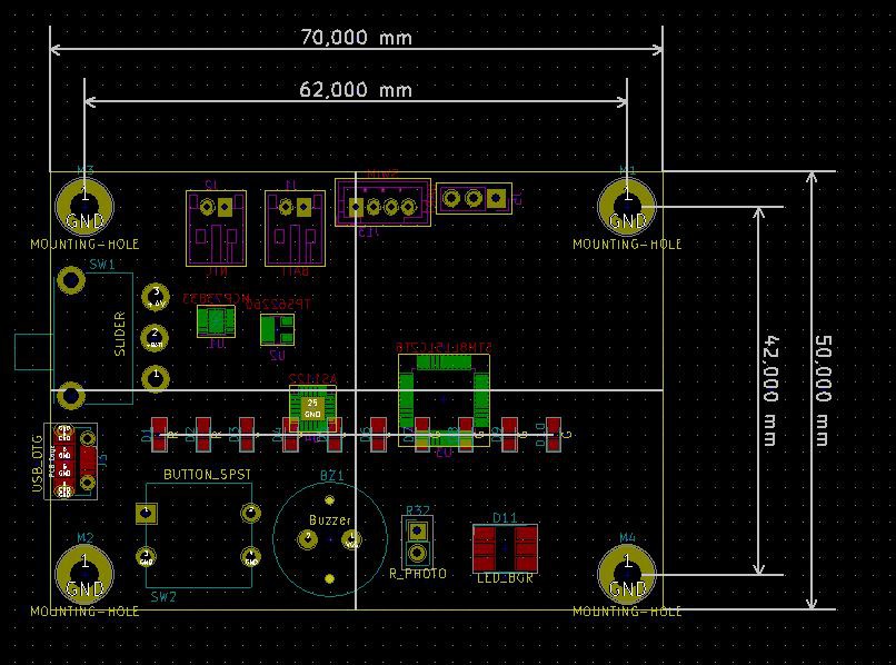
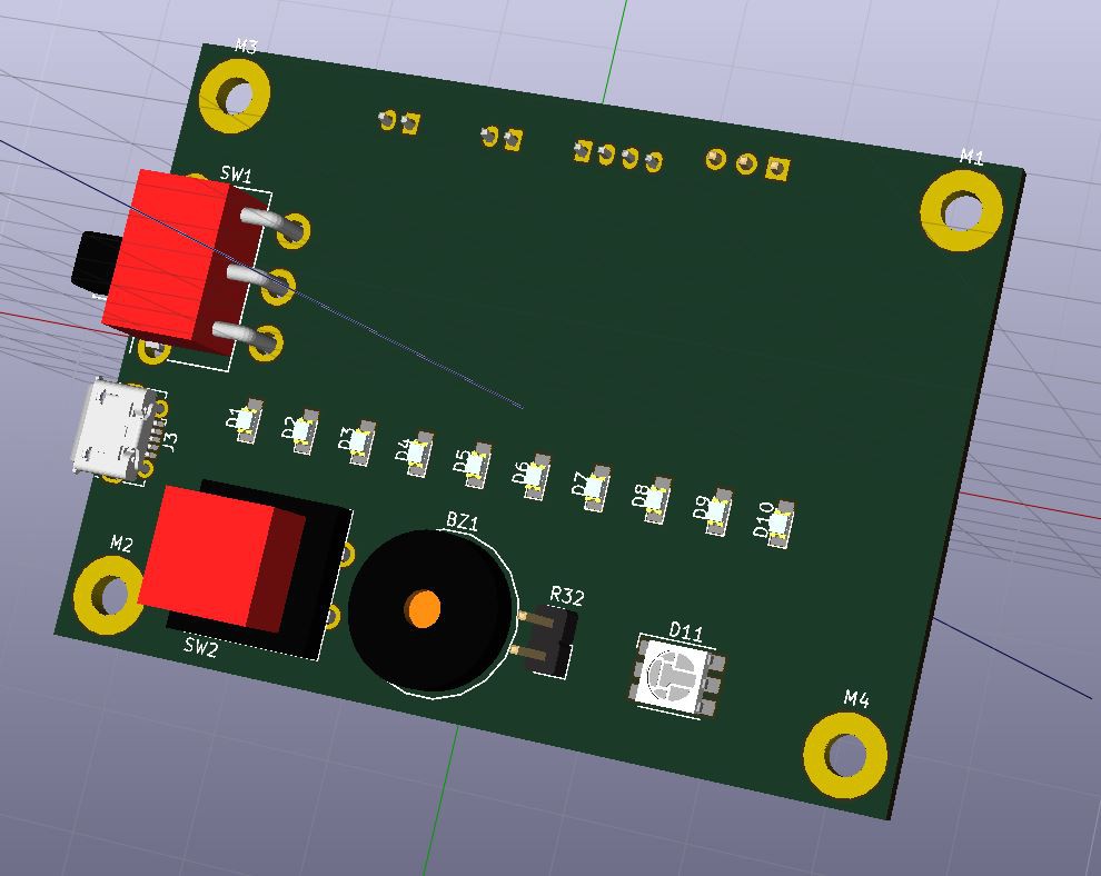
So I spent a few hours on creating footprints and 3D models for buzzer, slide switch, push button and other minor components. I wanted to have STEP models associated with WRL files, so that full 3D model can be exported. The 3D model will then be imported into Inventor, so that I can design a nice enclosure for the whole project.
When footprints were ready, I carried out initial components placement:

3D models are also visible in KiCad:

Next step is generating 3D model of the whole board (I use kicad StepUp plugin for FreeCAD - https://sourceforge.net/projects/kicadstepup/), which will be imported into Inventor. After that, I'll design initial enclosure and check if components placement is ok. When all main components placement is settled, I'll move on to PCB layout :)
 Luke
Luke
Discussions
Become a Hackaday.io Member
Create an account to leave a comment. Already have an account? Log In.