 Luke
LukeAs mentioned in previous log entry, I had to export 3D PCB model (with all major components), so that initial case design can be created. To do that, I used kicad StepUp plugin for FreeCAD. Exported STEP file was then loaded into Autodesk Inventor and I could start designing the case elements.
After a few hours of work, I had initial case design:
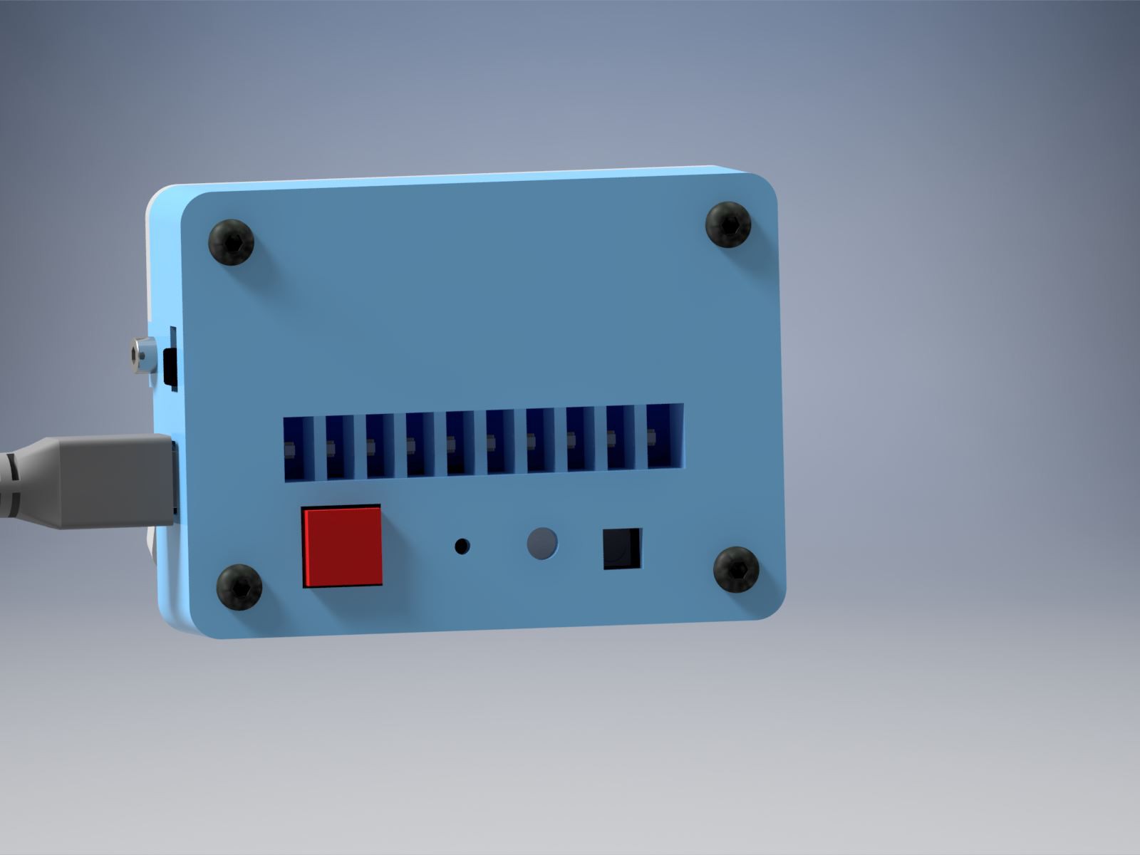
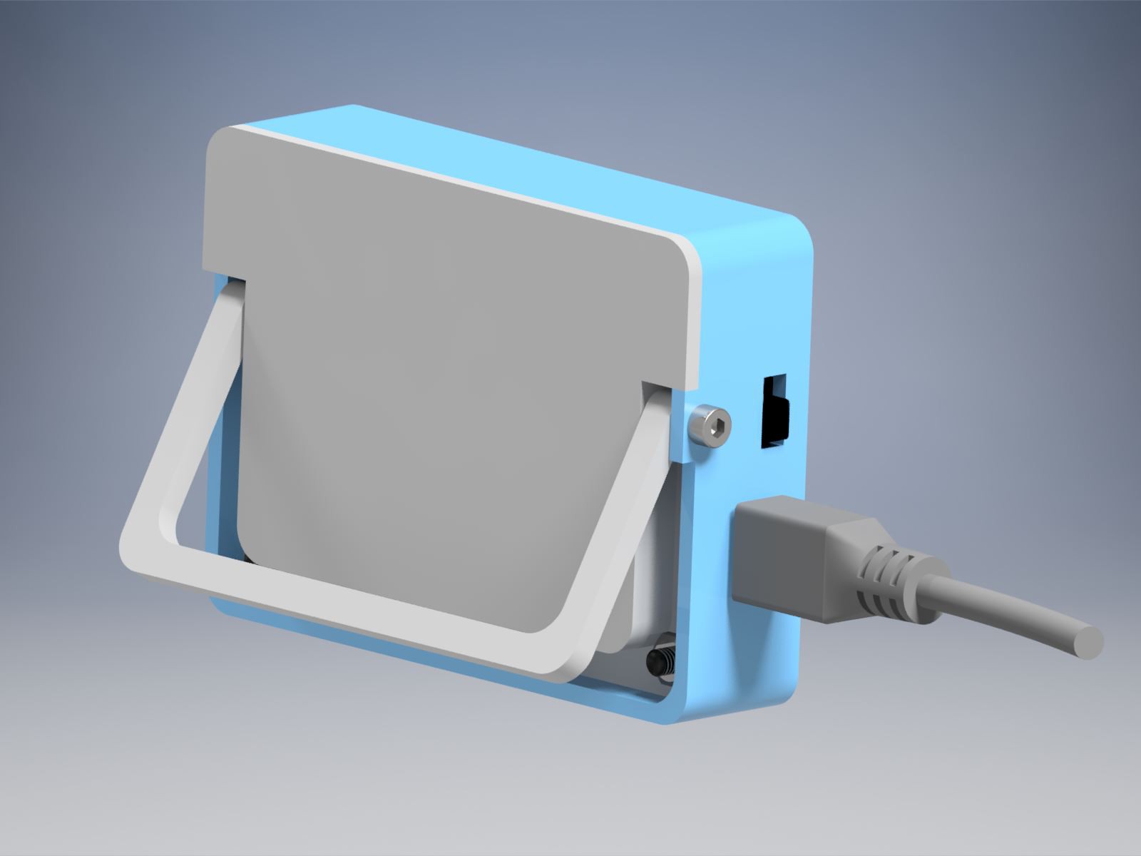
During the process I made small changes to components placement on PCB (like moving a switch a bit, etc.).
Now I could move on to PCB layout. I started with placement of all smaller components (like passives). The result is shown below (I'll take care of silkscreen later):
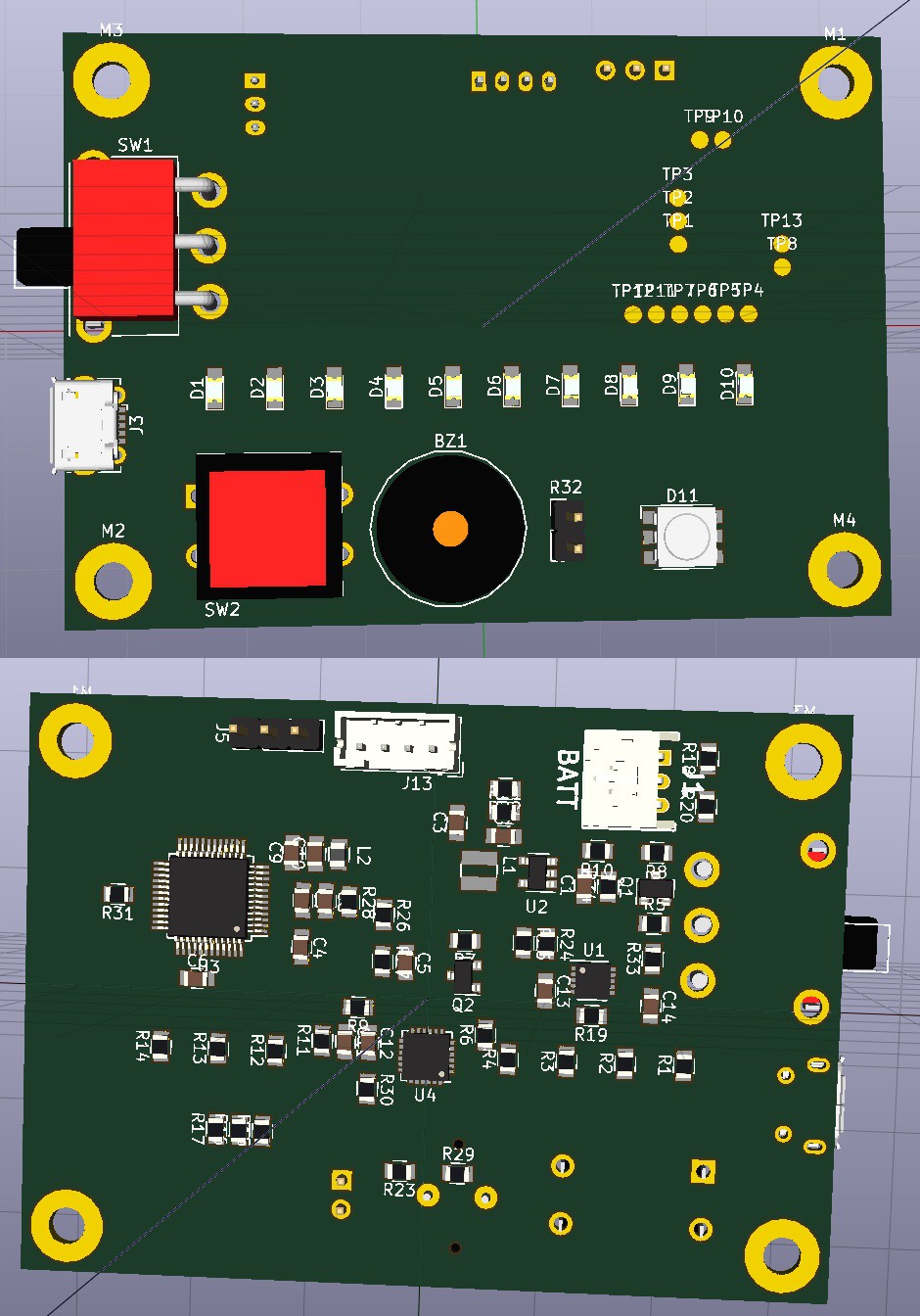
Next step is routing all the tracks :)
Discussions
Become a Hackaday.io Member
Create an account to leave a comment. Already have an account? Log In.