 Luke
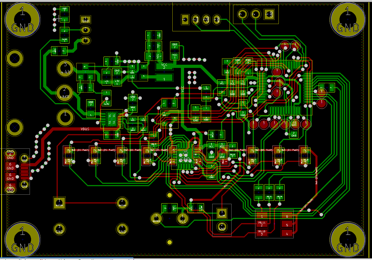
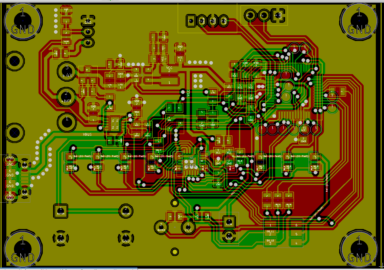
LukeSo today I finished layout of the PCB :) Together with components placement it took around 7 hours to finish. I had a small problem with ground plane - during routing I was not connecting GND pads of the components, so after creating GND plane pours on both layers I had to move some tracks around to create proper planes (also I added a few GND vias here and there).
PCB with filled areas display off:
PCB with filled areas display on:
Next step is generating production files (gerber files) and sending it to manufacturing :)
Discussions
Become a Hackaday.io Member
Create an account to leave a comment. Already have an account? Log In.