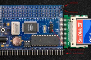
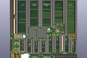
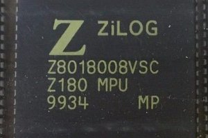
Z80 Single-board computer (with AVR controller)
Another Z80 single-board computer.
Another Z80 single-board computer.
To make the experience fit your profile, pick a username and tell us what interests you.
We found and based on your interests.
Wait_State_Generator-8Mhz-0ws_Live.pdfProgrammable wait-state generator, logic analyzer capture, 8MHz/0ws, M1 = 240nSAdobe Portable Document Format - 12.59 kB - 10/20/2016 at 21:37 |
|
|
Wait_State_Generator-8Mhz-7ws_Live.pdfProgrammable wait-state generator, logic analyzer capture, 8MHz/7ws, M1 = 1120nSAdobe Portable Document Format - 13.29 kB - 10/20/2016 at 21:37 |
|
|
Wait_State_Generator.jedProgrammable wait-state generator, JEDEC filejed - 4.42 kB - 10/20/2016 at 21:36 |
|
|
WSGEN-1V00.siProgrammable wait-state generator, logic equations- 2.67 kB - 10/20/2016 at 22:07 |
|
|
WSGen-1v00.PLDProgrammable wait-state generator, simulation input- 3.16 kB - 10/20/2016 at 22:12 |
|
|
Create an account to leave a comment. Already have an account? Log In.
Cool project. I gotta admit, though, I feel like your method for posting updates, here, doesn't lend itself well to others' commenting on your project.
Hi Eric:
Thanks for visiting and thanks for the complement. Comments can be added on the other site and do not require a user log-in to do so. Also, one can "follow" the updates to the project page by clicking on the "follow" button on the upper-right hand corner of all the posts,
If HACKADAY-IO's editor was a bit more project-meister-friendly for blog entries then I would keep everything here but alas, the editor allows no flexibility,
Peace and blessings.
Hardware test – 2nd phase - https://z80avrproject.wordpress.com/2017/01/24/hardware-test-2nd-phase/
PCB arrival – initial hardware check - https://z80avrproject.wordpress.com/2016/12/04/pcb-arrival-initial-hardware-check/
Update: Investigation into Z80 real-time debugging on the AVR - https://z80avrproject.wordpress.com/2016/11/22/update-investigation-into-z80-real-time-debugging-on-the-avr/
Project Reference: A "Modern Day" Z80 Hardware Emulator - https://z80avrproject.wordpress.com/2016/11/21/project-reference-a-modern-day-z80-hardware-emulator/
Additional thoughts on “debugging” Z80 code on the Z80 SBC. https://z80avrproject.wordpress.com/2016/11/19/additional-thoughts-on-debugging-z80-code-on-the-z80-sbc/
Project goals as thoughts and concepts now put into words … https://z80avrproject.wordpress.com/2016/11/19/project-goals-as-thoughts-and-concepts-now-put-into-words/
Success with FAT library! - https://z80avrproject.wordpress.com/2016/11/18/success-with-fat-library/
PC Board artworks off to the fabricator - https://z80avrproject.wordpress.com/2016/11/08/pc-board-artworks-off-to-the-fabricator/
Progress update - https://z80avrproject.wordpress.com/2016/10/28/progress-update/
Z80 testing – Simple program to exercise the UART - https://z80avrproject.wordpress.com/2016/10/23/z80-testing-simple-program-to-exercise-the-uart/
Getting the Z88DK software development suite up and running - https://z80avrproject.wordpress.com/2016/10/22/getting-the-z88dk-software-development-suite-up-and-running/
More testing of the memory and I/O address decoder PLD - https://z80avrproject.wordpress.com/2016/10/21/more-testing-of-the-memory-and-io-address-decoder-pld/
Programming the memory and I/O address decoder PLD - https://z80avrproject.wordpress.com/2016/10/20/programming-the-memory-and-io-address-decoder-pld/
Moving the programmable wait-state generator into a GAL22V10 - https://z80avrproject.wordpress.com/2016/10/18/moving-the-programmable-wait-state-generator-into-a-gal22v10/
1st attempt at a programmable wait-state generator - https://z80avrproject.wordpress.com/2016/10/14/1st-attempt-at-a-programmable-wait-state-generator/
Seems I have to actually post in order to get notices out to followers. Thanks for following. :)
Testing the AVR's interrupt latency: https://z80avrproject.wordpress.com/2016/10/10/103/
Folks:
I have been posting my progress on this project here: https://z80avrproject.wordpress.com/
It has a better editor than HACKADAY.IO and I seem to be able to add in-line photos as well. Honestly, I am not thrilled with either site's editing features.
Peace and blessings,
Scott
Sunday, October 9, 2016
I wired the 74HC299 onto a solderless bread-board along with my TEENSY 2.0++ running AttoBASIC V2.34 and a CD4511 driven 7-segment display connected to the outputs of the 74HC299. AttoBASIC [http://cappels.org/dproj/AttoBasic_V2_Home/Atto_Basic_V2_Home.html] makes a great development platform to test interface and operation of various devices while evaluating them. It beats repeated writing, debugging and downloading of code into the AVR. Once again, I found it instrumental in accomplishing the task at hand. Reading the datasheet can be a little confusing with regards to determining proper operation as a bidirectional parallel-to-serial and serial-to-parallel device. Since I am out of full 8-bit I/O ports on the AT90USB1286, this seemed the way to go and it comes in a 20-pin DIP or a 20-pin SOIC package. DIP for testing and SOIC on the PCB. Using SPI "mode 2" and setting the OE's and S1 low achieved the output function on the first try. After fiddling to find the right combinations of the states of S1 and OE, I was able to get my test code to work.
In short, the sequence is as follows:
Sequence to read from the bus;
1) Set S1=1 and OE=1
2) Perform a dummy SPI write (toggles the CLK line to load the registers with the state of the I[7..0] pins)
3) Set S1=0 to enable bit right shifting
4) Read data from the bus with an SPI read
5) Set S1=1 to end the bus read.
Sequence to write data to the bus;
1) Set S1=0 and OE=1 to enable bit right shifting
2) Perform an SPI write with the desired data
3) Set OE=0 to enable the output drivers
4) Set S1=1 and OE=1 to end the bus write and tri-state the pin drivers.
The AttoBASIC test code is as follows:
10 REM 74HC299 TEST
15 SDC7; SBC7 # OE=1 -> HI-Z
20 SBC6; SDC6 # (S0=1) S1=1 -> READ DATA
25 SPM 2 # SPI TO MODE 2
30 FOR N=0 15 # LOOP DIGIT TO DISPLAY
35 GOSUB 55 # WRITE TO BUS
40 GOSUB 65 # READ FROM BUS
45 NEXT; SPS # CONTINUE LOOP
50 END # END PROGRAM
55 CBC6; CBC7; PRI "N="; PRI N; SPW N # S1=0 -> SHIFT RIGHT OE=0 -> OUT TO BUS
60 SLP4; SBC6; SBC7; RETURN # WAIT, S1=1, OE=1 THEN RETURN
65 SPW 0; CBC6; PRI "DATA: "; PRX SPR; SBC6; RETURN #DUMMY WRITE, S1=0, PRINT BUS DATA, S1=1 THEN RETURN
Time spent was less than an hour.
Next up; determine if the AVR can emulate an 82C55A PIO.
Become a member to follow this project and never miss any updates
By using our website and services, you expressly agree to the placement of our performance, functionality, and advertising cookies. Learn More

 Plasmode


 Keith
Keith
your wiring job reminds me of building an oscilloscope on a breadboard for an embedded systems class using a ARM7 on a DIP PCB lol