Close
0%
0%

STEbus Z180 board

Z180 processor board

Similar projects worth following
Features:

Z180 or ZS180 processor
Two memory sockets
512K RAM
512K ROM
Two programmable serial ports
Two counter-timers
Boot ROM offers monitor, Forth, two Basics, CP/M, etc.

To be completed:

STEbus interface

Optional:

SD card interface
PCMCIA interface

The Zilog ZS180 seems to be the last member of the 64180 family in active production. 

For 33MHz clock max:
3 clocks per memory cycle = 11  MHz cycle rate. 
3 clocks per instruction = 11 MHz instruction rate (one opcode). 
6 clocks per instruction = 5.5 MHz instruction rate (one opcode, one data byte). 

32 MHz would be more convenient , as the STEbus needs a 16 MHz system clock.

I recently bought eight Z180 chips for £5. Rated at 8 MHz so only twice as fast as a 4 MHz Z80, but will be okay for most work. 

The Z180 would be useful for applications that would benefit from 1 megabyte of memory space, such as CP/M. However, I would use my PC for development work and Z80 systems as targets to run small applications. Therefore it might be more useful to develop a faster Z80 system than a larger Z180 system.

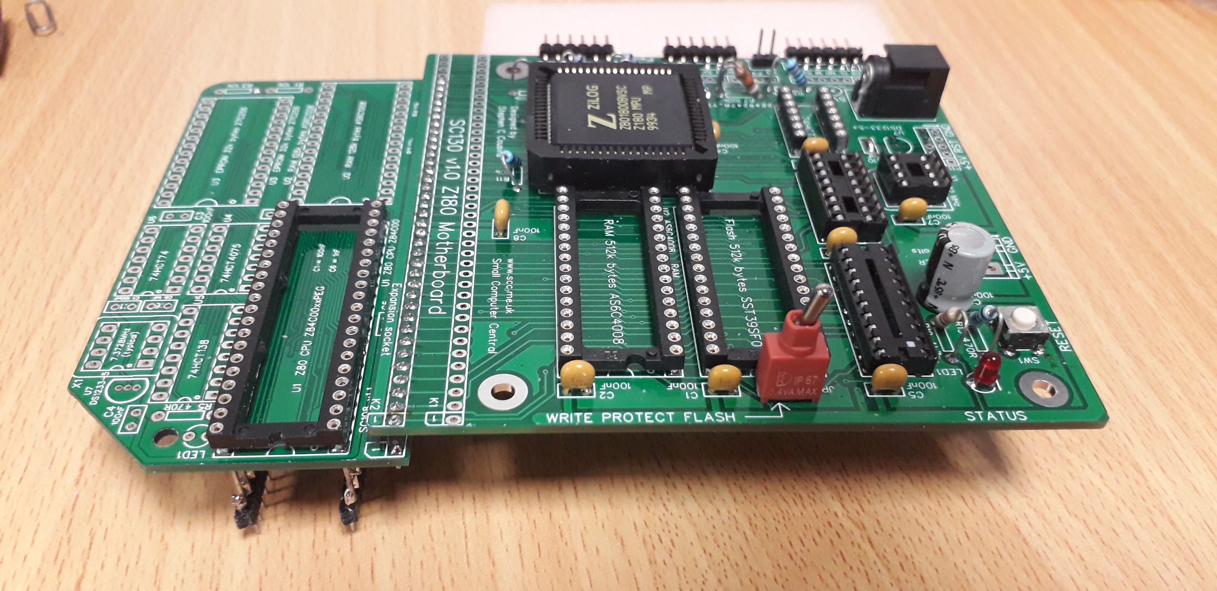
I considered using the existing SC130 board to avoid a lot of hand-wiring address, data and control buses. There is not much complicated going on there. The firmware is working with an overclocked CPU.

Ideally I would have liked an Arcom board because their PALs are not read-protected.

  • SC130 experiments

    Keith01/26/2024 at 20:18 0 comments

    I originally had the idea of making a Z180 to Z80 adaptor and then plugging the Z80 side into an STEbus Z80 board.

     Really inelegant and I suspect it would have added unreliability even if the idea was sound.
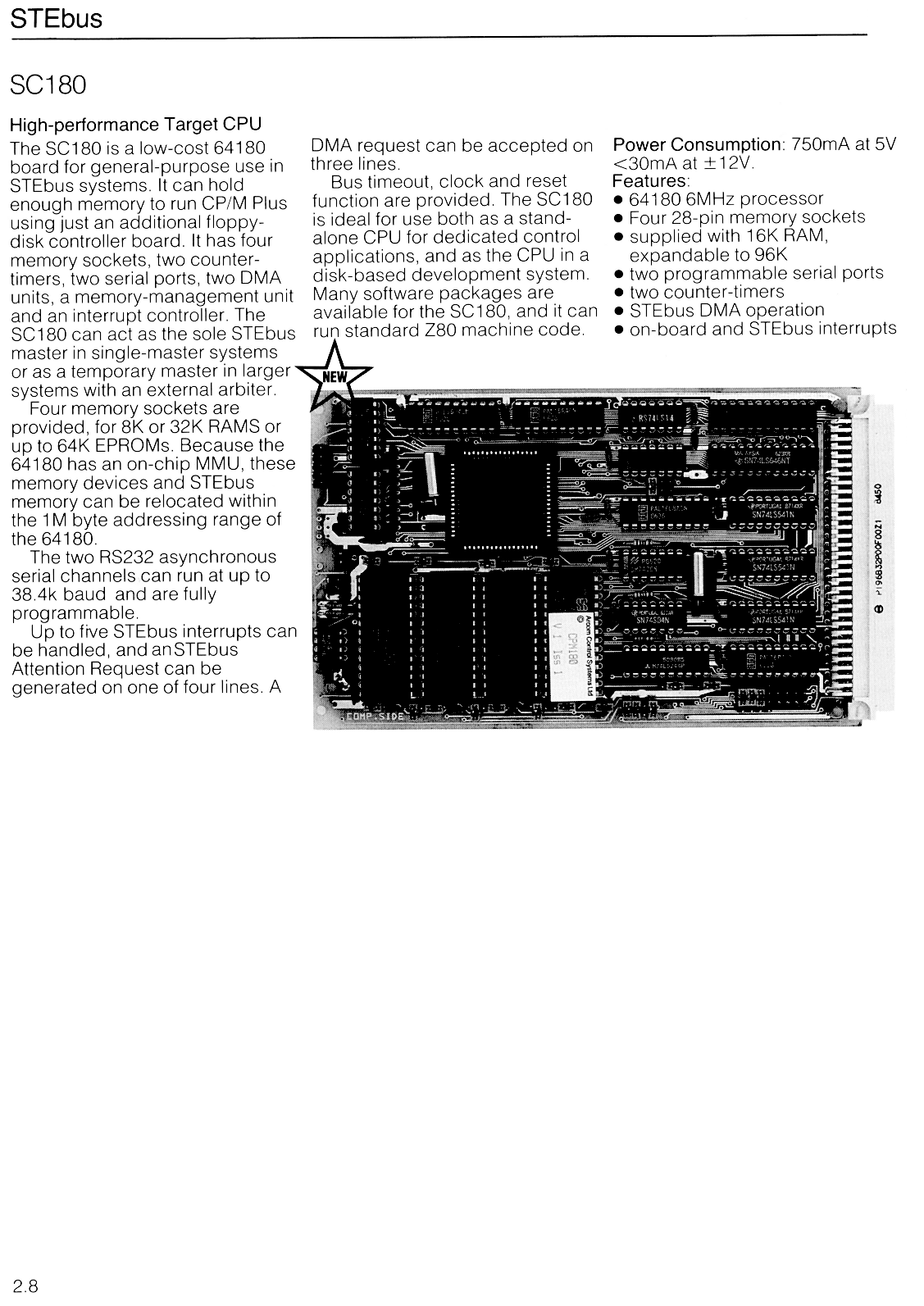
  • SC180 catalogue page

    Keith01/26/2024 at 20:05 0 comments

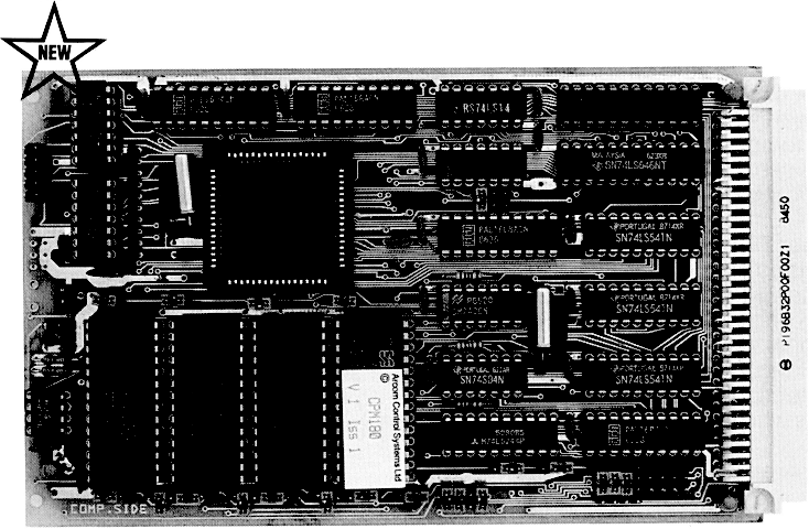
    The SC180 is a low-cost Z180 board for general-purpose use in STEbus systems. It has enough memory to run CP/M Plus. It has two counter/timers, two serial ports, two DMA units, a memory-management unit and an interrupt controller. The SC180 will act as the sole STEbus master in single-master systems or as a temporary master in larger systems with an external arbiter.

    Two memory sockets are provided, for 512K RAMs or up to 512K ROMs. Because the Z180 has an on-chip MMU, these memory devices and STEbus memory can be relocated within the 1M byte addressing range of the Z180.

    The two RS232 asynchronous serial channels can run at up to 38.4K baud and are fully programmable.

    Up to five STEbus interrupts can be handled, and an STEbus Attention Request can be generated on one of four lines. A DMA request can be accepted on three lines.

    Bus timeout, clock and reset function are provided. The Z180 is ideal for use both as a standalone CPU tor dedicated control applications, and as the CPU in a disk-based development system. Many software packages are available for the SC180, and it can run standard Z80 machine code.

    Power consumption: 5V only.

  • Project Log

    Keith05/19/2019 at 19:33 0 comments

    I had a think, and note that most of the control signals are exactly the same as the Z80. So rather than invent a new board from scratch, I could simply wire the Z180 to the CPU socket of an existing Z80 board (like the SCPUB board),

    GND, VCC, D0-7, A0-15, !WAIT, !BUSAK, !BUSRQ, !RESET, !NMI, !HALT, !RFSH, !IORQ, !MREQ, !M1, !WR, !RD are identical, and can wire directly to the Z80 socket.

    RTS0, CTS0, DCD0, TXA0, RXA0, CKA0/DREQ0, TXA1, RXA1, CKA1/TEND0, TXS, RXS/CTS1, CKS are serial port signals that can connect to FTDI USB cables or serial port drivers.

    A16-A19 are new but uncomplicated, just extra address lines. They would have to go to large memory chips via flying wires.

    Z80 CLK of Z80 --> EXTAL
    PHI is the CPU clock output.

    Z80 INT --> INT0
    INT1, INT2 are extra interrupt lines, not needed yet.

    DREQ1, TEND1 are for DMA which I can ignore for now.

    E is for Motorola peripherals which I don't have.

    ST works with !HALT and !M1 to indicate CPU state. New states are DMA, HALT, and SLEEP.

    XTAL (crystal drive) is not used because CLK is driven.

    This doesn't look too difficult to deal with.

    Transplanting the Z180 into the existing SCPUB board could be done without having to re-write the serial port drivers. There is no reason why the existing SCC chip must be replaced by the Z180 serial ports. The BASIC interpreter ROM can continue to use the SCC.

    For a completely new board, one would want to do without the SCC for reasons of economy but I shan't be doing that just yet.

    2020-07-09

    Had an idea. I could join a Z180-to-RC2014 board to an RC2014-Z80 board to get a Z180-to-Z80 adapter. It would save me hours of hand-soldering many wires, and it can be readily recreated.  So I ordered them.

    It then occurred to me that most of the pins are address and data, which go to the memory sockets, which have most pins in common with my STEbus Z80 board's memory sockets. Add power and ground, that is 26 pins. Still leaves 14 pins to wire to the Z80 socket. I think I will go with the two-stage adaptor idea. If nothing else, the first stage might let me drive RC2014 boards from the host board. Not elegant or robust, but okay for experiments.

    2020-07-10

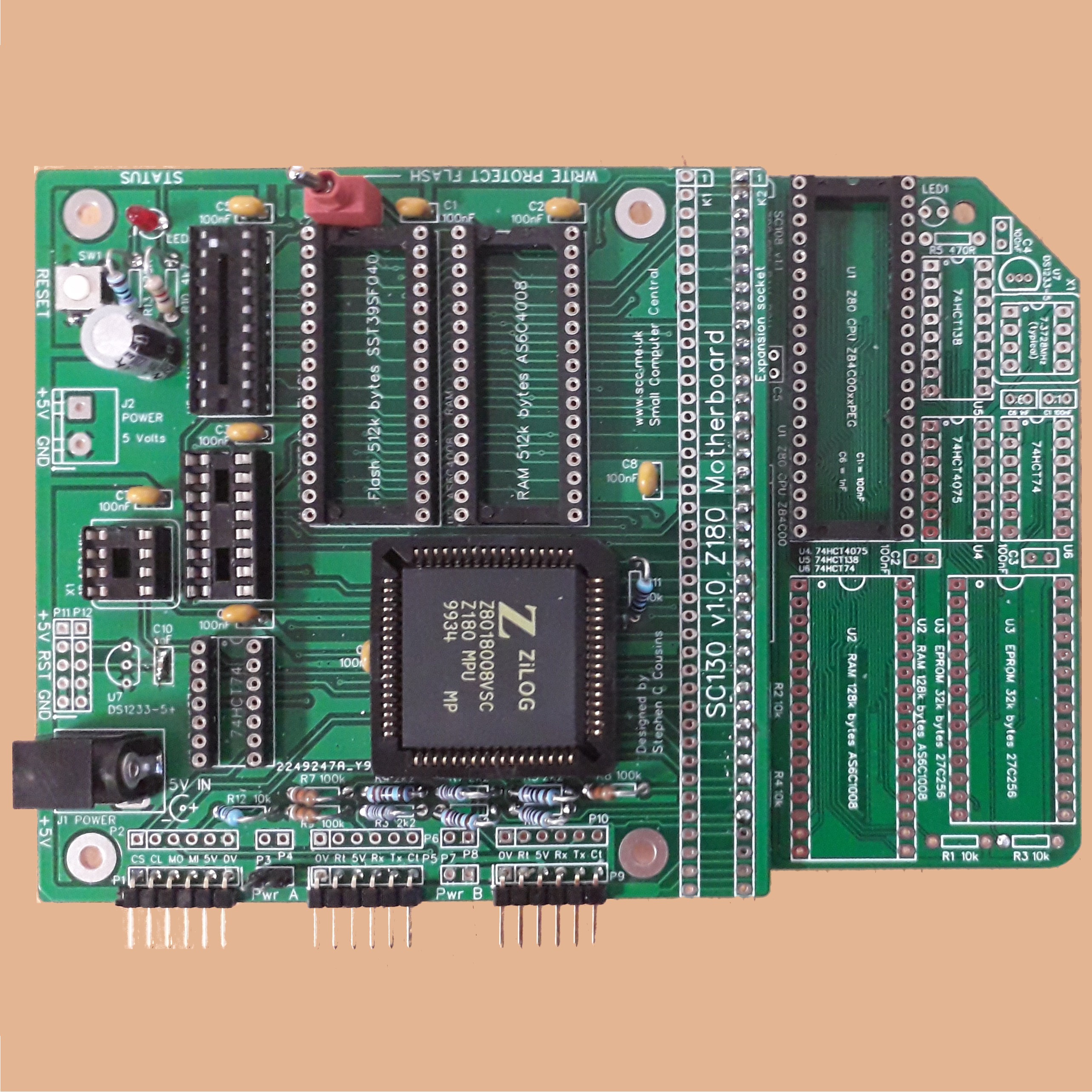
    The SC130 Z180 board arrived.

    2020-07-13

    The Z180 board was quickly populated with resistors, capacitors and sockets at lunchtime. I aim to get it running on its own first, as a basic sanity check. I am short of a reset chip, 74LS688 and a 74LS139. I will have to borrow them from other projects.

    2020-07-14

    The SC108 Z80 board arrived.

    2020-07-15

    Boards joined together. Quick buzz-check, the power, ground, D0-7 and A0-7 are correctly connected between the memory sockets of one board to another, so I am confident most other pins are. One critical issue is that the STEbus board uses the /WAIT pin to make the CPU wait while the STEbus cycle is in progress. The two RC2014 boards both tie it inactive high to 5V. These had to be isolated from 5V and joined from board to board. Amazingly, the RC2014 bus does not include this signal! The STEbus board uses /INT for the DART and CTC, and /NMI can be driven from the bus. The SC180 board ties both high, so that needs dealing with.

    The conjoined boards were photographed, and the photos added to the project gallery. 

    First step will be to see if the STEbus board and Z80 will work with the adaptor kludge boards between them. 

    2020-07-22

    The Z180 uses addresses 00-3F for on-chip peripherals, which conflicts with the host board's I/O map. So the host board logic will need modification. The SC130 has a full memory map, 512K RAM and 512K ROM. This leaves no room to access the STEbus memory space. I have fitted 512K RAM (KM684000BLP-7L) and have some 256K ROM (AT49F002T70PC). The SC130 firmware (ROMWBW) is 512K, I will see if it really needs all that space.

    Since it is easier, cheaper and faster to fit large memory chips on board, the STEbus is rather redundant for memory expansion. Bus...

    Read more »

View all 3 project logs

Enjoy this project?

Share

Discussions

Similar Projects

Does this project spark your interest?

Become a member to follow this project and never miss any updates